|
|
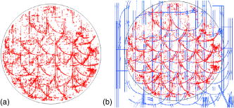
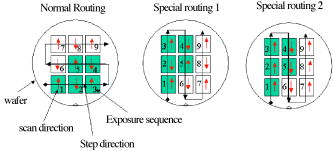
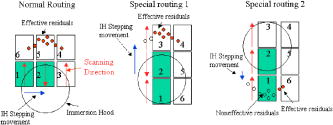
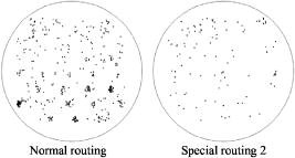
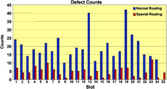
1.IntroductionImmersion lithography is required to produce circuits with a 65-nm minimum half-pitch and then 45-nm, and possibly 32-nm, half-pitches with double patterning, unless double patterning is used prematurely for the 65-nm half-pitch, jacking up cost and complexity. Although 193-nm immersion lithography was developed at an amazing pace—a functioning chip was made less than 1 year1, 2, 3 after the introduction of tool—it still needs tremendous effort to meet the extremely tight specifications for the 45-nm node. One of them is defect density, which needs to be as low as one defect per wafer pass if many device layers are exposed with immersion scanners. Unfortunately, the liquid coupling medium seems more likely to carry particulates than the air coupling medium, whether these particles are from materials on the wafer or from the exposure system itself. Besides particles, bubbles and watermarks are the other two important defect types induced by a liquid medium. Well-designed immersion systems together with hydrophilic materials can prevent production of bubbles. Post-exposure soak or a carefully selected resist/topcoat can prevent watermarks. Even using just topcoat can greatly reduce the number of harmful particles after development. Unfortunately, none of the above methods can prevent the printing of particles deposited before exposure. This paper reports a unique special routing technique to reduce the number of particle-printing defects to a single digit per wafer. Several champion wafers in a wafer lot contain one defect per pass. 2.Possibilities of Particle PrintingThe immersion hood (IH) is an important component of immersion scanners for supplying, confining, and draining the water during exposure. It is circular in shape, placed under the bottom lens element. Its edge is outside the exposure field. Hence, the area of coverage of the immersion fluid is larger than the exposure field. To confine the immersion fluid, there is an air knife surrounding the IH with an inward-oriented force in the radial direction, preventing water leakage to the outside of the immersed area during wafer movement. Since particle printing is an important defect cause for immersion lithography, it is necessary to identify where the particles come from and how they are printed. The first possibility considered is printing the particles suspending in water near the resist surface. By considering the 500-mm/s wafer scan speed and the flow rate of water, the particles in water are almost static during exposure while the wafer quickly passes by underneath. The resist image would consist of stripes if particles in suspension were printed. However, stripe-like defects have never been observed. The second possibility is that particles are transported through water from the IH to attach to the wafer surface and those inside the exposure slot are printed. There is no direct evidence for or against the existence of this type of defect. Nevertheless, there is no way to prevent them from printing, except to entirely eliminate particles in the water. A third possibility is that particles left from the previous exposure fields may be printed. They may be left when the water droplet leaks out of the IH during the wafer scan. There is indeed water leak during the wafer scan. Water leaks will take place if the IH is not designed properly, if the scan speed is too high, or if the wafer surface is too hydrophilic. Figure 1 shows the wafer-defect distribution accumulating on the defect map of 20 bare-silicon test wafers; the 20 bare-silicon wafers are hydrophilic, and the resulting leakage of IH is high at hydrophilic surfaces. Straight-line and arc trajectories are clearly observed. Water can leak along the tangential directions at the edge of the IH along its path of travel, since the water at the IH edge is constrained only in the radial direction. Besides water leakage in tangential directions at the IH edge, the IH tends to leak more, caused by the inertial force during stage acceleration, especially at the rear edge while the stage is starting to move, leading to an arc-shaped defect distribution. Hence, the defect map shown in Fig. 1 consists of straight lines and arcs from vertical and horizontal movements, respectively. The vertical direction is the wafer scanning direction. 3.Special RoutingsSince the particle-printing defects are supposedly created by printing the particles left over from the previous scan, we will classify the residuals as effective and noneffective corresponding to whether they are printed in subsequent fields. As shown in Fig. 2 , since the hood is larger than the exposure field, it is possible that residuals are left from more than one neighboring field and printed in subsequent exposures. To overcome this problem, we used specific routings for immersion exposure. Figure 3 shows a normal exposure routing and two special routings. In a normal routing, the fields are exposed row by row and the scan operates in alternating upward and downward directions, so that the time used to move back the reticle can also be used to expose the wafer, thus upholding productivity. The scan directions are perpendicular to the field-stepping directions. Our special routing exposes the fields column-wise with scan directions parallel to the field-stepping directions. Special routing 1 shown in Fig. 3 has opposite scan directions alternately assigned in a column, while the scan directions are all parallel to the field-stepping directions for special routing 2. Figure 4 shows the advantages of the special routings. The defect count from normal routing should be higher than that from special routing 1, which is in turn is higher than that from special routing 2. Fig. f2Effective residuals and noneffective residuals. The effective residuals are left by field scan B, while the noneffective residuals are left by field scan A.  4.ResultsFigure 5 shows the defect maps for two wafer lots with identical exposure conditions except for a difference in routing, namely normal routing and special routing 2. The defect distribution is evidently dependent on exposure routing. Figure 6 shows the defect count. The data show large defects reduction, 4.8 per wafer on average with special routing 2 compared to 19.7 per wafer with normal routing. This special routing technique indeed works. Another study using special routing 1 confirms our expectation that its defect count is between that of special routing 2 and that of normal routing but is closer to the former. 5.Concluding RemarksIn summary, this paper reveals a unique technique that can significantly reduce the defect count in immersion lithography. Defect reduction with special routing 1 is also observed, but it is slightly less than that with special routing 2. However, since the wafer stage does not have to wait for the reticle stage to move back, the throughput for special routing 1 is higher than that of special routing 2. The choice of these two routings depends on careful consideration of the tradeoffs between wafer yield and scanner productivity. ReferencesB. J. Lin,
“Pushing the limits of optical lithography,”
(2004) Google Scholar
(Dec. 2,
(2004) Google Scholar
J. H. Chen,
“Characterization of ArF immersion process for production,”
Proc. SPIE, 5754 13
(2005). 0277-786X Google Scholar
|