|
|
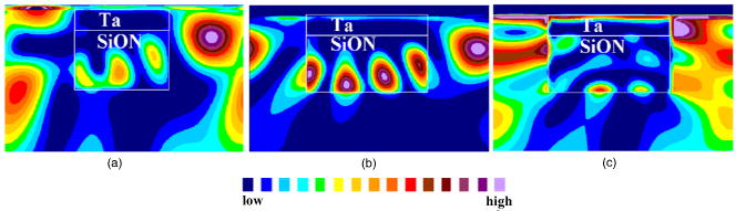
1.Observation of a Resonant-Type AnomalyStarting from a range of mask linewidths for a given pitch, we determine, for each mask linewidth, the exposure dose needed to print the line/space grating to a fixed target CD, i.e., the dose to size. In general, the dose-to-size curve is expected to increase monotonically as the mask linewidth increases. However, we have detected a local enhancement in such a dose-to-size curve for a bilayer attenuated phase shift mask (att.PSM). The experiment is conducted with a mask consisting of a 34-nm-thick Ta layer with a 113-nm-thick phase-shift layer on top—referred to as 1% att.PSM—containing a -oriented grating of 360-nm pitch. (All dimensions at mask level.) The grating is exposed at NA 1.20 using cQuad (opening angle) 0.96/0.8 (outer/inner sigma) -polarized illumination. The wafer target is a 45-nm CD at 90-nm pitch. For these settings, the mask transmission resonance occurs as a sharp peak on top of the smoothly increasing dose-to-size curve between 40- and 50-nm mask linewidth (at ), as presented in Fig. 1 . This resonant-type anomaly is well predicted by rigorous electromagnetic field (EMF) lithographic simulators, and is thus fully described by the Maxwell equations. The experimental observation of this anomaly validates in fact the predictive power of lithographic simulators for the imaging performance of even this type of exotic mask stacks. Fig. f1Observation of a mask transmission resonance (indicated by an arrow) through mask linewidth at pitch (at ) for 1% att.PSM using NA 1.20 cQuad 0.96/0.8 (outer/inner sigma) -polarized illumination. Right axis: experimental dose-to-size curve. Left axis: simulated amplitudes of the propagating diffraction orders for the -oriented poles using -polarization. 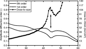 Simulations reveal this resonance effect already in the off-axis diffraction spectrum as a local transmission loss in the propagating diffraction orders (see Fig. 1). Both zeroth and first diffraction orders exhibit a dip in their amplitude leading to an increase of the required dose. 2.When Does the Mask Transmission Resonance Occur?Because of its substantial impact on the dose-to-size behavior, we have examined the dependency of the mask transmission resonance on various mask and lithographic settings. First, we observe multiple mask transmission resonances through mask linewidth for a large pitch range. Figure 2 compares the dose-to-size curves from simulation to those from experimental printing evaluation for a pitch range of to targeted to a 45-nm wafer CD. Resonances around mask linewidths , , and become apparent. The pitch influences only the magnitude of the resonance. Fig. f2Top: simulated dose-to-size curves through mask linewidth for a pitch range of to . Bottom: corresponding experimental printing results for a pitch range of to . Results for 1% att.PSM using NA 1.20 -oriented dipole 0.96/0.8 sigma outer-inner -polarized illumination. 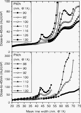 Second, we have investigated the effect of the mask material and stack on the resonance at the same lithographic conditions as for the 1% att.PSM. We did not find a resonance anomaly in the standard mask stacks binary mask and 6% att.PSM. We also have looked into the behavior of two bilayer att.PSM versions with Ta as absorber, but as transparent phase shifter. These masks have a Ta thickness of or with a corresponding thickness of or , respectively, on top. Experimentally, we do not observe a resonance in these att.PSM for pitch . This is an indication that the mask transmission resonance is not related to the -metal absorber alone, but is more likely created by the mask stack configuration of a dielectric layer on top of the absorber. Indeed, if we perform by simulations a thickness variation of or on any absorber layer such as Ta, Cr, or even , we can find a thickness of the transparent layer that will generate a resonance around one or more specific mask linewidths. For example, at NA 1.2 using -oriented dipole 0.96/0.8 (outer/inner sigma) with -polarized illumination, a thickness around on top of 19-nm-thick Ta layer produces a mask transmission resonance, while at 145-nm thickness, no anomaly in the dose-to-size curve is seen [see Fig. 3a ]. Fig. f3Impact of the dielectric layer thickness on the presence of a mask transmission resonance in the simulated dose-to-size curve using -oriented dipole illumination, other settings as in Fig. 1. (a) For att.PSM with 19-nm Ta-absorber using -polarized light. (b) For att.PSM with 34-nm Ta-absorber using -polarized light. 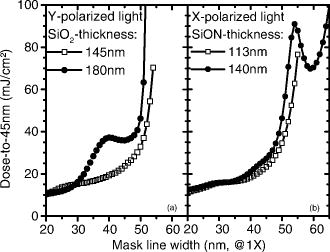 Last, the magnitude of the mask transmission resonance depends on the NA, illuminator shape, and polarization state of the incoming light, but the resonant-type anomaly appears at all investigated settings. For both - and -polarized light, resonances occur, but at different parametric mask settings. Figure 3b illustrates that at the thickness, where a resonance occurs for -polarized light (cf. Fig. 1), no resonance is observed for -polarized light. However, by increasing the thickness, the mask transmission resonance starts emerging at the large linewidth side. As such, the mask configuration acts as a polarization-sensitive filter. These findings support the idea of an optical resonance induced by the transparent phase-shift layer of the mask grating. This phenomenon seems closely related to the waveguide-grating resonances described in Refs. 1, 2. The resonances occur due to the coupling of the diffracted fields from the incoming light into the waveguide modes. In our case, the absorber grating creates the diffracted fields, and the waveguide is formed by the dielectric layer of higher refractive index between the quartz substrate and air of lower refractive index. For a certain mask linewidth, the dielectric cavity becomes a resonator for one polarization direction. Looking at the transmission of the EMF under off-axis incidence through the mask, as exemplified in Fig. 4 for 1% att.PSM, we observe spots of higher intensities confined inside the -cavity for the resonant mask linewidth using -polarized illumination, in contrast to the nonresonant mask linewidth and in contrast to -polarized illumination. 3.Impact on Mask Error Enhancement FactorThe sharp enhancement of the dose-to-size curve around the resonant mask linewidth will induce a variation in the mask error enhancement factor (MEEF) behavior. We even measure negative MEEF values caused by a mask transmission resonance (see Fig. 5 ). A negative MEEF seems counterintuitive since it implies that the printed wafer CD decreases with increasing mask linewidth at fixed exposure dose. Moreover, the correlation between the dose-to-size curve and MEEF behavior clearly indicates that the MEEF behavior can be well predicted by the differential of the dose-to-size curve through mask linewidth. This can be simply explained as follows. MEEF is defined as the derivative of the wafer CD through mask linewidth, or with =mask linewidth. Multiplying the right side of Eq. 1 by unity, or givesFig. f5Settings identical to Fig. 1. Top: experimental dose-to-size curve; bottom: experimental MEEF curve and differential of the experimental dose-to-size curve. 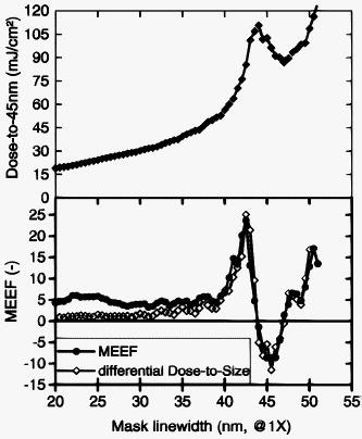 The wafer CD variation through exposure dose is assumed to correspond to a first-order function for small dose variation based on simulations and experiments specific to this study, in other words, is a constant, and Eq. 2 results in the proportionality More precisely, when the dose-to-size curve decreases with increasing mask linewidth, a negative MEEF is measured, which is consistent with the negative slope of the dose-to-size curve around these mask linewidths. Figure 5 is an experimental proof of the relationship Eq. 3 between dose to size and MEEF for the specific conditions of this study, showing a MEEF oscillation from to over only a 2-nm mask linewidth increase at . The occurrence of strong varying MEEF within the current limits of mask linewidth uniformity is of course an undesirable imaging effect, as it will give rise to uncontrollable CD variations at fixed exposure dose. On the other hand, understanding the mechanism of the mask transmission resonance can offer the possibility to explore potential imaging applications.4.ConclusionsIn this letter, we have demonstrated the existence of mask transmission resonances under specific lithographic conditions of mask stack, line/space grating, and illumination. Experimental investigations have revealed the presence of such mask transmission resonance as an irregularity in the dose-to-size behavior through mask linewidth. As a consequence, even negative MEEF values were reported. Furthermore, we have argued that the differential of the dose-to-size curve through mask linewidth corresponds to the MEEF. In addition, the agreement between our experimental and simulated results confirms the validity of mask 3-D simulations for the conditions of this study. We conclude this letter with a two-part remark: First, caution is required when exploring alternative mask stacks for improving imaging to exclude uncontrollable and thus unwanted optical anomalies. Second, the awareness of these optical effects could possibly translate into a controllable and thus beneficial impact on imaging. However, the implementation has yet to be proven viable. ReferencesR. Magnusson and
S. S. Wang,
“New principle for optical filters,”
Appl. Phys. Lett., 61
(9), 1022
–1024
(1992). https://doi.org/10.1063/1.107703 0003-6951 Google Scholar
G. Bao and
K. Huang,
“Optimal design of guided-mode grating resonance filters,”
IEEE Photonics Technol. Lett., 16
(1), 141
–143
(2004). https://doi.org/10.1109/LPT.2003.818927 1041-1135 Google Scholar
|