|
|
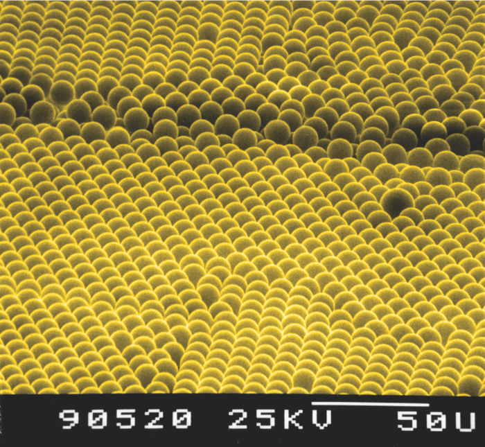
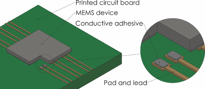
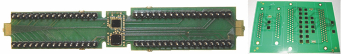
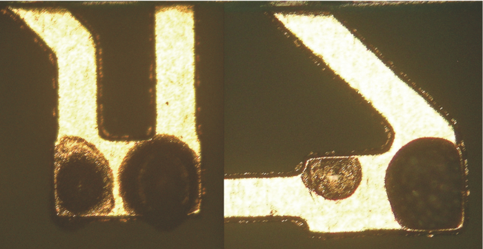
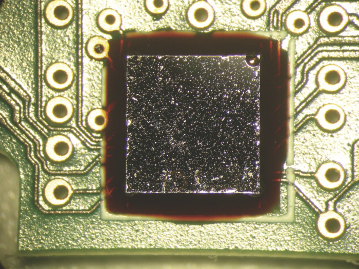
1.Introduction1.1.Conductive AdhesivesIsotropic conductive adhesives (ICAs) have been used in electronic applications for more than 40 years. Traditionally, ICA has been a mix of nonconductive adhesive, typically of epoxy type, with silver particles or flakes. However, to reduce cost, other conductive particles have also been used like carbon, copper, and nickel. Designing an ICA requires optimization of a number of factors including final electrical conductivity, rheological properties during application, total metal content (a cost issue in the case of noble metals), and thermomechanical properties.1 To make an ICA using a nonconductive matrix, the volume fraction of conductive filler particles needs to reach and exceed a certain level, called the percolation threshold. That is, the amount of particles must be sufficient to create at least one path of particle–particle contacts, and hence conduction through the entire adhesive. This threshold is dependent on the shape of the particles. Given the traditional flake-like conductive particles, the percolation threshold will also depend on the orientation of the flakes. In a typical microelectronic application, both the application of the adhesive and the shear applied during placement of the component cause a significant orientation of the flakes,2 as illustrated in Fig. 1. Fig. f1Illustration of the tendency for metal flakes (in this case silver) to align themselves in parallel with the die and substrate.  In practical use, the rheology of the adhesive is a critical parameter that determines the applicability of the material. As the filler content increases, the viscosity of the two-phase material increases. This limits the amount of filler that can be applied without using solvents to reduce the viscosity. However, the shape of the particles also has a very strong influence on the rheology.3 This means that for some optimal shapes, you can add a much larger volume fraction of filler particles without increasing the viscosity beyond practical values. Traditionally, ICA materials have suffered from brittleness caused by the large fraction of metal particles with very different thermomechanical properties than the adhesive matrix. Thermal expansion mismatch as well as the large difference in compression modulus between filler and matrix causes high local strain, and typically creates nucleation centers for cracks in the material. Adding flexible molecules to the adhesive matrix can reduce brittleness and improve thermal cycling behavior. However, a reduced glass transition temperature and increased moisture uptake are unfavorable side effects. 1.1.1.Metallized polymer spheresA novel idea for improvements of the ICA material properties is to replace the solid metal flakes by highly uniformly shaped metal-coated polymer spheres. A potential drawback of using spheres in ICAs is the significantly higher percolation threshold. This is, however, more than overcome by the fact that much less than one tenth of the particle volume is actual metal. This introduces the possibility of using noble metals like gold at a reasonable cost. As the viscosity increase due to the addition of sphere fillers is very modest compared to adding flake-like particles, there is no need for solvents to optimize viscosity. Instead, choosing oligomers with suitable molecular weight can optimize viscosity of the resulting ICA. Both the spherical shape, and the fact that the thermomechanical properties are very similar to the adhesive matrix, reduces the local stress in the filler-matrix interface. A scanning electron microscope (SEM) photograph of metalized polymer spheres is shown in Fig. 2. Several opportunities arise in terms of optimizing the conductive filler properties. A highly controlled size distribution of particles can be made with one or more particle sizes to optimize the filler fraction. Different core materials can be designed with different mechanical properties and glass temperature (Tg). This means that the conductive fillers can be used as the component for mechanical energy absorption needed in, e.g., a shock environment. 1.2.Harsh Environments and Reliability DemandsThe electronics in ammunition fuzes are subjected to a number of demanding environmental conditions. When fired, medium caliber ammunitions such as 30 mm×173 are subjected to a setback acceleration pulse with an amplitude exceeding 60,000 g. As the projectile travels through the barrel, the rifling imparts a spin on the projectile resulting in a centripetal acceleration, which increases radially by 9000 g/mm. The metal-to-metal contact between the projectile and barrel can also result in severe shocks and vibrations. After 4 ms, the projectile exits the barrel. At this point the pressure propelling the projectile is abruptly removed, which can result in mechanical oscillations in different structures such as the packaged electronics. In some cases, the fuze electronics must also operate after the projectile has penetrated a hard target. In addition, the fuze and its electronics must be capable of remaining safe and operable in severe climatic conditions where temperatures can range from –54° to 71°C. 1.3.Packaging ConceptDirect chip-on-board packaging concepts, where the MEMS device is mounted directly to the printed circuit board (PCB), is highly favorable for medium caliber fuze applications due to the limited space available. This packaging concept can provide a high integration density at a low manufacturing cost compared to the traditional concept, where numerous process steps are performed to mount the MEMS device in a package, which again is mounted onto a PCB by soldering, for example. Electrical and mechanical interconnect technology is, however, challenging for chip-on-board packaging concepts. Patterned ICA is one technology that can be used for interconnection in a chip-on-board packaging concept. Figure 3 illustrates the proposed ICA-based packaging concept presented in this work. 2.Experiment2.1.Preparation of AdhesivesThe isotropic conductive adhesives were based on EPO-TEK®353ND epoxy adhesive manufactured by Epoxy Technology (Billerica, Massachusetts). The adhesive is a two-component adhesive, with a glass temperature of approximately 90°C. Two different metallized polymer spheres have been used in the present study to make two different ICAs, denoted ICA-A and ICA-B, respectively. For ICA-A, 30-μm polymer spheres with a thin silver coating were mixed together with the epoxy. The ICA-B contains 4-μm polymer spheres coated with nickel and gold. The volume fraction of metal-coated spheres in the adhesive was about 50%. A small adjustment of the particle content was made to improve the printing properties. No solvents or surface additives were added to the adhesive. The metallized polymer spheres were mixed into the adhesive manually by gradually adding the particles until the wanted concentration was achieved. 2.2.Design and Manufacturing of Test Structures and Test BoardTo characterize the properties between the PCB and the MEMS interconnect, we designed “dummy” MEMS test structures with no movable parts. These were fabricated on the same wafers as the real MEMS devices. The MEMS test structures were fabricated using a silicon-on-insulator (SOI) substrate with a 43-μm-thick device layer and a 2-μm-thick buried oxide layer (BOX). The layout of the test structures used in this experiment is shown in Fig. 4. The nomenclature of the test structures denotes the shape of the conducting area, and the width of the trench between these areas. The size of the test structure is 3.5×3.5 mm2. The I-100 test structure has 12 pads with a size of 250×350 μm2, while the I-20 test structure has 32 pads with size 100×350 μm2. Fig. f4Layout of the I-100 (left) and I-20 (right) test structure. The pads are shown in the layout. 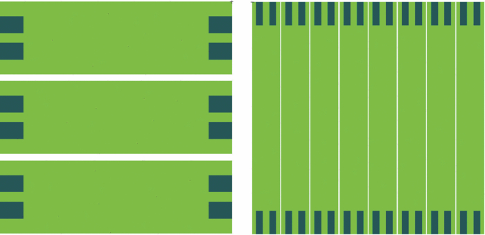 A PCB suitable for both recovery firing tests as well as other environmental tests was designed. A photograph of this board is shown to the left in Fig. 5. The board is made of FR4 laminate with Tg = 125°C. On each side of the board, two test structures as well as four 0402 resistors can be mounted. One side of the board is designed for I-100 test structures, while the other side is designed for test structures with smaller pads and finer pitch.4 On each side, one test structure is rotated 90 deg with respect to the other test structure. The pads and conductors on the PCB have a thickness of approximately 50 μm, ∼45-μm-copper, and ∼5-μm-nickel. In addition a ∼100-nm-thick layer of gold is chemically deposited on top of the nickel layer. The board includes contact points for Kelvin measurements of the contact resistances prior to firing tests. On each test structure, it is possible to do Kelvin measurements of four contact resistances. When the test structures are placed inside the 30-mm projectile, the firing board is cut where the notches are shown in Fig. 5. The size of the board placed inside the projectile is 9×16 mm2. After cutting the board, Kelvin measurements on the test structures can still be done using a probe station. In the following section, this board is denoted as the firing board. Previously, we had designed a PCB to measure contact resistances for several I-100 test structures as well as resistances on daisy-chain structures.5 A photograph of this PCB is shown to the right in Fig. 5. This board is denoted “temp board” in the following sections. 2.3.Stencil Printing of the AdhesiveThe adhesive was printed onto the firing boards by using a Dima (Deurne, The Netherlands) HS-100 stencil printer. The stencil was manufactured by HP Etch (Järfälla, Sweden) and was covered with nickel/teflon. Nickel/teflon has a significantly lower surface energy than the pure metal and therefore significantly reduces the adhesion between the adhesive and the edges of the holes and the bottom side of the stencil. The thickness of this stencil is approximately 50 μm over the printing areas. Figure 6 shows a picture of the adhesive printed onto the firing boards where the I-100 test structure will be mounted. The 30-μm polymer spheres used in ICA-A are clearly visible in the right picture in Fig. 6. The total bond area for the test structure was estimated to be approximately 1.05 mm2. This represents only approximately 9% of the chip area, which is very small, and thereby increases stresses in the bonds during the environmental testing. Fig. f6Picture showing stencil printing of ICA-B (left) and ICA-A (right) onto the firing boards (I1 through I8). 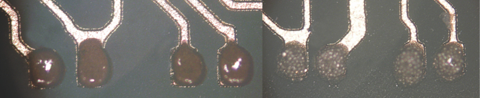 For shear strength testing of the ICA interconnects, eight temp boards were used. When printing adhesive on these boards, a 125-μm-thick steel stencil was used where the pad openings were made by laser cutting. The pad size was 250×350 μm2. Figure 7 shows a photograph of the varying quality stencil printing results obtained using this steel stencil. 2.4.Mounting of Test Chips onto Test BoardsEight boards were mounted, denoted I1 through I8, with I-100 test structures. Table 1 gives the relationship between the boards used, type of ICA, and number of test structures on each board. Table 1Relationship between the I1 through I8 boards, number of components mounted on each board, and ICA used for mounting the components. ICA-A uses 30-μm silver-coated spheres, while ICA-B uses 4-μm gold-coated spheres. The stencil used when printing adhesive had a thickness of approximately 50 μm.
For shear strength testing of the ICA interconnects, eight temp boards, denoted S1-S8, were mounted with five test structures each. Table 2 gives an overview of the board numbers, number of components used, and type of ICA used on each board. Since there were not enough I-100 test structures available for the shear testing experiment, I-20 test structures were used instead. The I-20 test structures were rotated 90 deg, so the pads on the temp board are along the conductive path of the I-20 test structure. The width of the conductive paths on the I-20 test structure is 420 μm, which is larger than the length of the pads (350 μm). Since no electrical measurement is performed on these boards, it was acceptable to use the I-20 test structure for this purpose. Table 2Overview of the S1-S8 boards used for shear testing and the type of ICA used. The temp board is used for this experiment, and the stencil is used when the printing adhesive had a thickness of 125 μm.
A My-9 pick-and-place machine from MyData (Täby, Sweden) was used for placing components on the boards. The same low mounting pressure was used when placing all the test structures onto the boards. Curing was performed at 150°C for one minute. It should be noted that no underfill has been used when mounting the test structures to the boards. 2.5.Environmental TestingDegradation of interconnection points will be accelerated by environmental conditions like static and dynamic temperature stress, as well as mechanical impact in the form of shock and/or vibration. In the current work, thermal cycling and firing tests have been performed to investigate the impact on the interconnect the reliability. 2.5.1.Thermal cycling testsThe thermal cycling stress test is a simple way to investigate the effect of thermally induced stress on the interconnect reliability. We kept one board of each type as virgin samples for reference purposes. For all boards except for boards used as virgin samples, rapid thermal cycling stress in the form of air-to-air thermal shock cycling has been performed between –55 and +125°C in a Heraeus (Thermo Scientific,Wattham, Massachusetts) HT 7012 S2 thermal cycling chamber. The tests have been performed according to military-standard (MIL-STD)-883 G method 1010.8 test condition B. Test objects were exposed to four cycles per hour, 50% duty cycle, and load transfer time within 60 s between temperature extremes. Selected samples were exposed to 10 and 100 thermal cycles. Electrical resistance was recorded on units after TC stress and compared to values obtained prior to stress. 2.5.2.Recovery firing testsAfter the temperature cycle tests, selected samples were mounted into 30-mm projectiles, and recovery firings were performed. These firing tests were carried out at Nammo Test Center at Raufoss, Norway. The inner diameter of the projectile is 17.7 mm. The PCBs were mounted inside the projectile, together with a suitable potting material. Figure 8 shows a photograph of the projectile before and after firing. A Bushmaster II cannon was used for firing. Recovery was achieved by firing the projectile into a stack of porous wallboards about 4 m long. The distance from the cannon to the wallboards was approximately 100 m. When leaving the muzzle, the speed of the projectile is about 1040 m/s. During the flight, the reduction of speed is negligible. Since the stopping distance in the wallboard is approximately the same as the barrel length, the resulting negative acceleration is assumed to have the same order of magnitude as the setback acceleration during launch. However, since the projectile tumbles violently inside the wallboards, the direction of the acceleration becomes very random. Fig. f830-mm projectile used for test firing. Bottom picture shows the projectile ready to be fired. To the right, a recovered projectile is shown. 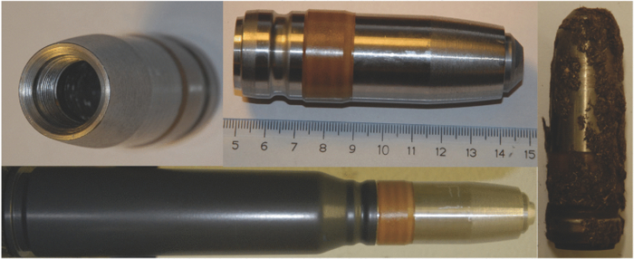 The I1 to I4 boards, together with the S6 board used for shear test, were mounted into the 30-mm projectile and recovery firings were performed. Before firing, but after the temperature tests, underfill was added to one test structure on each of the I1 to I4 boards, as shown in Fig. 9. Hence, it would be possible to determine if this would improve the performance during the firing test. 2.6.CharacterizationThe integrity of the adhesive bonds can be an issue when the bond is exposed to environmental stress, like long-term exposure to elevated temperatures, thermal excursion, and /or mechanical impact. Destructive die shear testing is a simple and fast method to check bump integrity for bonded dies. Test objects were fixed in a bracket socket, and a shear head elevated over the substrate surface was forced horizontally to a lateral edge of the MEMS test structures. Shear height should be sufficient to avoid the bonding material and sufficiently low enough to not influence the actual strength of the bond. Furthermore, movement of the shear head should be perpendicular to the side of the chip to avoid chip damage and thereby influence the recorded measurement. Shear strength and failure category were of interest as a reliability monitor of the mounted test structures. Shear test measurement was performed using a DAGE (Aylesbury, United Kingdom) 2400A shear tester with a D10-kg die shear load cartridge. Shear test was performed at 10-μm/s shear speed at 150-μm shear height. Shear test was performed prior to and after the thermal cycling test, and on samples exposed to thermal cycling and firing tests. Samples were cross sectioned and analyzed at each stage of the applied stress test. The devices were embedded in epoxy resin under vacuum (15 to 20 kPa). They were grinded with SiC paper up to grade 4000 and water lubrication with emphasis on precise cross sectioning through a series of MEMS to PCB interconnection points. Finally, the devices were polished on medium hard cloth with alcohol-based lubricant with diamond grade 6 and 3 μm. Light microscopy was performed with a Neophot 32 microscope (Zeiss, Jena, Germany). 3.Results and Discussion3.1.Characterization by Electrical Measurements3.1.1.Initial contact resistanceA summary of the contact resistances for the I-100 structures prior to the environmental tests is presented in Table 3. The test structures mounted with ICA-A display a higher resistance compared to the test structures mounted with ICA-B. This difference can be explained by the thin silver layer coating of the polymer spheres for ICA-A, which is less than 50 nm thick. This is considerably thinner than the corresponding gold layer coating on the polymer spheres for ICA-B. Another effect contributing to the higher resistance for ICA-A is the partial delamination of the silver from the polymer spheres (see Fig. 10), which may have been caused by the manual mixing of spheres and adhesive. This delamination is caused by low adhesion between silver and polymer spheres. An improved adhesion can be obtained by actively modifying the surface of the polymer spheres. This has been shown by compression testing of the metallized spheres.6 Table 3Average initial contact resistances and standard deviation for I-100 test structures mounted with ICA-A and ICA-B.
3.1.2.Contact resistance after temperature testsThe average contact resistances after the temperature cycle tests are shown in Table 4 for the I1 to I4 boards. Table 4Average contact resistances before and after temperature cycling for I-100 test structures mounted with ICA-A and ICA-B.
None of the contact resistances failed during the temperature tests. As can be seen from Table 5, the change in contact resistance is much more pronounced when the samples are exposed to 100 temperature cycles than ten temperature cycles. For ICA-B, the electrical resistance decreases for the first ten cycles. This can possibly be explained by minute mechanical movements between the spheres, causing a more intimate mechanical contact by breaking up tarnish films. This effect has been reported for mechanical cycling of similar metallized polymer spheres.7 A similar mechanical interaction between the silver-coated spheres may also be the cause of the encountered delamination and cracking of the silver layer mentioned before. It is noteworthy that the change in contact resistance after 100 cycles is approximately equal for both types of ICA. Table 5Comparison of measured average contact resistances after temperature cycling and after firing tests, respectively, for I-100 test structures.
3.1.3.Contact resistance after recovery firing testsThe average contact resistances before and after recovery firing tests are shown in Table 5. 27 out of 32 contact resistances passed the firing test. For the ICA-B-type adhesive, the contact resistance changes are almost identical, regardless of the number of temperature cycles. For the ICA-A adhesive, the samples exposed to 100 temperature cycles show an increase in contact resistance after firing, while the samples exposed to ten temperature cycles show a decrease in contact resistance. However, the number of measured resistances on boards I2 and I4 are five and six respectively. This is due to cracking of components during test firing. Therefore, the average resistance value after temperature cycling for these boards will deviate from the values given in Table 4, where the average values are calculated using eight contact resistances. All the components that cracked were without underfill. On board I2, the Raverage after firing is calculated from measuring four contact resistances on a structure with underfill, and one resistance on a cracked test structure without underfill. The most interesting observation is that the contact resistance on the I2 board actually decreased after the firing test. On this board, one contact resistance on the cracked structure was measured. This resistance shows a large decrease in resistance value after firing (–29.9%). The cracking of the component will significantly reduce the mechanical stress in the interconnects and might be a reason for the observed resistance decrease. However, the average change on the four other contact resistances on the structure with underfill is still negative, –3.2%. Resistance measurement was done on some samples during temperature cycling tests. Using the recorded data, the temperature coefficient of resistance during temperature cycling was of the order of 0.0025 K−1. When measuring the resistance after temperature cycling and firing tests, the room temperature may have changed a few degrees Celcius, since some days elapsed between the measurements. However, the TC of the resistances is too small to explain the measured resistance change. The effect of having underfill during a firing test is shown in Table 6. Table 6Change in resistance during firing tests for test structures with and without underfill. Both boards have been exposed to 100 temperature cycles prior to firing tests. The underfill was added after the temperature cycling. Four resistances are measured in each case.
The results here show clearly that underfill is very favorable with respect to resistance change as a result of firing. It is noteworthy that the ICA-A contact resistance with the test structure with underfill decreases after firing, and that change is almost identical to the change on the I2 board with the test structure having underfill. Adding an underfill will set the ICA interconnects under compression due to curing shrinkage. In addition to reducing the mechanical stress in the interconnects during the firing tests, this can probably explain the small and even negative change in the contact resistance. 3.2.Characterization by Shear TestingSummary data from shear test measurement performed on virgin samples and samples exposed to thermal cycling and firing test are presented in Tables 7, 8 for ICA-A and ICA-B, respectively. Measured data are presented in gram force (gf). Test samples mounted with ICA-A displayed lower shear strength and higher standard deviation compared to the corresponding result obtained for samples mounted with ICA-B. Furthermore, lower shear strength was recorded for virgin samples compared to samples exposed to thermal cycling for the ICA-A samples. Table 7Die shear test result for ICA-A.
Table 8Die shear test result for ICA-B.
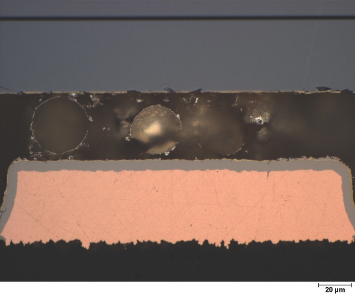
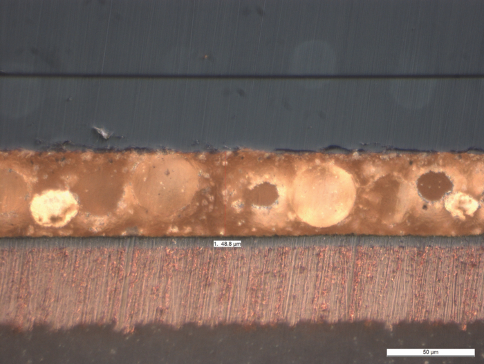
Light microscopy examination of shear tested ICA-A samples revealed distinct differences in the deposited amount of adhesive from sample to sample, with less deposited adhesive observed on virgin samples compared to samples exposed to thermal cycling. The ICA-B samples displayed high bond strength with no notable decrease in bond strength recorded for samples exposed to thermal cycling. Samples exposed to firing tests after ten thermal cycles displayed higher bond strength compared to samples not exposed to firing. The large standard deviation for ICA-A and the unlikely improved bond strength for ICA-B after firing tests are contributed to variations in contact area caused by the stencil printing process combined with the limited number of samples. The predominant failure mode from shear test was observed to be fracture in the adhesive close to the die interface for all samples, except samples, after 100 thermal cycles, where the predominant failure was observed to be fracture within the Si chip itself. No samples with mounted ICA-A were available for testing after ten TC and firings. 3.3.Characterization by Cross SectioningSelected samples were cross sectioned and analyzed by light microscopy and scanning electron microscopy (SEM). Figure 10 presents an image of an I-100 test sample mounted with ICA-A. This sample displays a gap of ∼40 μm, corresponding to approximately 1.3 sphere diameters. This image also shows patches of the plated silver that has delaminated from the polymer spheres. Test samples with ICA-B display a gap in the order of ∼10 μm, corresponding to two to three sphere diameters, as shown in Fig. 11. The cross sections show that the resulting adhesive thickness at the pad area is approximately 40 μm for ICA-A and approximately 10 μm for ICA-B, even though both samples are mounted with the same force. For ICA-A, the adhesive thickness seems to be controlled by the sphere diameter, whereas for ICA-B, the squeeze film effect defines the minimum thickness. An experiment performed with smaller pads shows that this squeeze film effect is reduced, resulting in an adhesive thickness approaching the sphere diameter.4 The cross section on one of the pads on the S8 board is shown in Fig. 12. The test structure is mounted using ICA-A. As previously mentioned, a stencil with thickness ∼125 μm was used when printing the adhesive to the board. As seen from Fig. 12, the adhesive thickness is approximately 50 μm, which is approximately 10 μm thicker than for the test structures on the I1 through I8 boards mounted with ICA-A. 3.4.DiscussionA considerable amount of work was spent on achieving a proper printing of the adhesive. The printing quality is dependent on several factors such as the quality of the stencil, the pressure and speeds of the squeegee, and rheological property of the adhesive such as viscosity and shear thinning properties. As seen from Fig. 7, the quality of the printing is not as good as it should be. This will reflect the variation in the shear test results. This variation in the printing process is probably the main cause of the large standard deviation obtained in the shear test, as well as that the samples exposed to ten TC and firing tests showed a higher shear strength than, e.g., the virgin samples (see Table 8). Shear force degradation is generally expected to be more severe for thin mechanical joints compared to thicker joints, as there is a reduced volume for absorbing the applied mechanical energy. Increasing adhesive joint thickness from ∼40 to 50 μm is therefore expected to slightly improve shear force result as well as performance to thermally induced stress and mechanical shock. Hence, the shear properties for the test structures mounted with ICA-A on the I1 to I8 boards is expected to be slightly lower than the results shown in Table 7. A rough (but probably conservative) estimate of the maximum strain in the adhesive can be made, assuming that the glass temperature of the adhesive represents the zero-stress condition for the mounted test structures. This means that maximum strain will occur at the minimum exposure temperature during the temperature cycling. The test structures are 3.5×3.5 mm2, which means that the maximum distance to the neutral point of the chip is approximately 2.5 mm. The coefficient of thermal expansion (CTE) mismatch is approximately 15 ppm/°C. Due to the small area of adhesive, we also assume that the adhesive itself absorbs all the strain. This is obviously a very conservative estimate. The shear deformation calculated from these numbers corresponds to approximately 5 μm. In the case of the thin interconnections obtained for the ICA-B adhesive, the shear deformation is roughly half of the interconnect thickness. Such a thin adhesive interconnection will have negative effects on thermal cycling performance as well as on mechanical shock tests due to the reduced volume for absorption of mechanical energy. It was observed that the large 30-μm spheres used acted as spacers, increasing the gap between the die and the substrate pads. The result was more than three times an increase in bond thickness, and hence a significant reduction in shear strain. In the present experiments we have used silver and gold metallization systems. In addition, the tests have been performed without adding humidity. We therefore expect the degradation of the contact resistances to be mainly due to mechanical interaction, either particle—particle or particle—contact pad. Due to the nature of the epoxy matrix, we expect that these interactions are strongest at elevated temperatures, above the Tg. Due to nonlinearity, the net effect will be an increased particle separation, increasing the contact resistance. However, during initial temperature cycles this can have more of a rubbing effect, causing a more intimate metallic contact and hence a reduced contact resistance. Also, additional curing of the adhesive can cause an initial reduction in contact resistance. Adding underfill to some of the test structures before the firing tests gave reduced degradation of the contact resistances. Adding underfill to the test structures before temperature cycling would force the chip and PCB to expand at the same rate, and hence reduce the strain in the interconnect. In addition, the curing shrinkage in the underfill adds a compressive stress in the ICA. This would probably increase the mechanical strength to the structure, providing enhanced performance to temperature cycling, mechanical shock, and vibration. 4.ConclusionDirect chip-to-board MEMS to PCB interconnect using isotropic conductive adhesive with metallized polymer spheres as electrical conductive filler material displays capability as a viable interconnect technology for rough environment applications such as medium caliber ammunition fuzes. The highly accelerated thermal cycling tests and realistic firing tests that are performed show excellent performance of the ICAs with no notable shear strength degradation and acceptable changes in electrical contact resistances. The adhesive printing process needs to be refined for both types of adhesives. As a result, the shear tests show a significant difference between the ICA-A and ICA-B. The other variations in the results can also largely be contributed to variations in the stencil printing process. This investigation shows that isotropic conductive adhesive based on metallized polymer spheres can be suitable for direct chip-to-board interconnection of a MEMS device in a fuze application. By implementing such a packaging concept, a higher packaging density and reduced cost can be achieved. AcknowledgmentsPart of this work has been sponsored by the Norwegian Research Council grant number 187971/140 and the Norwegian MoD. The authors want to thank Joachim Moe Graff at Sintef and Thorkild Kaasa, Tone Somme, Oyvind Froyland, and Atle Skaugen at FFI for their most valuable assistance during this work. ReferencesJ. e. Liu,
(1999) Google Scholar
A. Bjorneklett,
L. Halbo, and
H. Kristiansen,
“Thermal conductivity of epoxy adhesives filled with silver particles,”
Intl. J. Adhesion Adhesives, 12 99
–104
(1992). https://doi.org/10.1016/0143-7496(92)90030-Y Google Scholar
W. S. Lee,
I. Y. Han,
J. Yu,
S. J. Kim, and
K. Y. Byun,
“Thermal characterization of thermally conductive underfill for a flip-chip package using novel temperature sensing technique,”
Thermochimica Acta, 455 148
–155
(2007). https://doi.org/10.1016/j.tca.2006.11.034 Google Scholar
J. Gakkestad,
P. Dalsjo,
H. Kristiansen,
R. Johannessen, and
M. M. V. Taklo,
“Use of conductive adhesive for MEMS interconnection in military fuze applications,”
Proc. SPIE, 7592 75920I
(2010). https://doi.org/http://spie.org/x648.html?product_id=840890 Google Scholar
H. Kristiansen,
M. M. V. Taklo,
J. Gakkestad,
P. Dalsjo,
R. Johannessen,
F. Oldervoll, and
V. H. Nguyen,
“Development of low modulus conductive adhesive for MEMS interconnects,”
306
–310
(2009). https://doi.org/http://www.smta.org/knowledge/proceedings_abstract.cfm?PROC_ID=2643 Google Scholar
J. Y. He,
T. Helland,
Z. Zhang, and
H. Kristiansen,
“Fracture of micrometre-sized Ni/Au coated polymer particles,”
J. Phys. D: Appl. Phys., 42 085402
(2009). https://doi.org/10.1088/0022-3727/42/8/085402 Google Scholar
H. Kristiansen,
U. Brudberg, and
M. Gulliksen,
“Electrical and mechanical properties of metal-coated polymer spheres for anisotropic conductive adhesive,”
63
–71
(1999). Google Scholar
BiographyJakob Gakkestad received his MSc and PhD in electronics from the University of Oslo in 1985 and 1993, respectively. In 1985 he worked as an ASIC designer at Sintef ICT in Oslo, focusing on the design of mixed signal ASICs in BiCMOS and CMOS technology. From 1997 to 2002, he worked at Tandberg Data, where after some time he became manager for the hardware development department. He also worked as a senior analog asic designer at Chipcon (now TI) before he joined the Norwegian Defence Research Establishment (FFI) in 2003. At FFI he is working with electronics and MEMS for gun-launched munitions fuzes. Per Dalsjo received his first MSc degree in mechatronic engineering from the University of New South Wales, Sydney, Australia, in 2001. After working several years as a mechanical engineer, he returned to university, completing a MSc degree in electronic engineering specializing in MEMS at the University of Oslo, Norway, in 2007. Since 2007 he has worked as a research scientist at the Norwegian Defence Research Establishment (FFI) on MEMS systems for gun-launched munitions fuzes and the integration of electronics and mechanics in such fuzes. Helge Kristiansen received his MSc in solid state physics from the University of Oslo (UiO) in 1988. In 1988 he was working at Sintef ICT, previously the Center for Industrial Research with Electronic Packaging. He received his PhD in experimental particle physics from UiO in 1996, and held a part time position at Chalmers from 1999 to 2004. His main field of research was the use of adhesives, thermal management, and instrumentation systems. In 2004 he joined Conpart AS as CTO, where he is involved in the characterization and application of polymer particles for use in electronic applications. Rolf Johannessen received his PhD in physical electronics from the University of Oslo, Norway, in 2008. From 1989 to 2005 he was focusing on materials and processes for harsh environment applications at the Research and Development Department of Getech and the technology department of Alcatel Space Norway, Horten, Norway. He also held a position as educational staff at Horten College of Engineering, Norway. From 2008 to 2010 he was with SINTEF ICT, Oslo, Norway, as a research scientist where he was working on failure mechanisms and packaging technology for harsh environments, focusing on high temperature applications. Currently he is on his leave from SINTEFICT in a new position as manufacturing process leader at GE Vingmed Ultrasound, Horten, Norway. Maaike M. Visser Taklo worked for one year with optical sensors as a project engineer at AME AS in Horten, Norway, in 1997. She received her PhD degree in physical electronics from the University of Oslo in 2002. The topic of her thesis was wafer bonding for MEMS. She was employed by the microsystems and nanotechnology department at SINTEF in 1998, where she works today as a senior research scientist and is responsible for their wafer bonding activities. She has several years of experience as a project leader for research projects focused on packaging technologies for MEMS. Through her engagement in the projects e-CUBES and JEMSiP-3D, 3-D integration of MEMS has become one of her main areas of expertise. |
|||||||||||||||||||||||||||||||||||||||||||||||||||||||||||||||||||||||||||||||||||||||||||||||||||||||||||||||||||||||||||||||||||||||||||||||||||||||||||||||||||||||||||||||||||||||||||||||||||||||||||||||||||||||||||