|
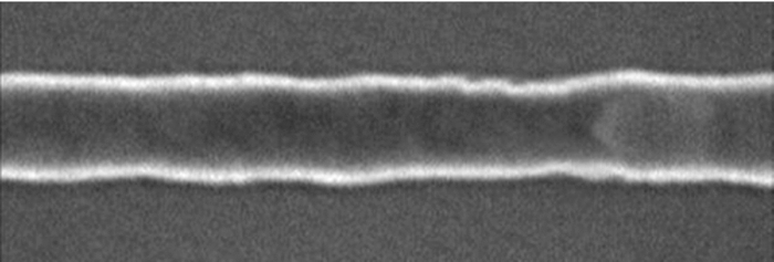
It seems likely that the ultimate resolution of most projection and direct-write lithography schemes is limited by line-edge and linewidth roughness (LER/LWR). In the sub-50-nm feature size regime, line-edge roughness is already consuming a considerable amount of the overall feature size control budget (Fig. 1) and having measureable impact on device performance. At the 32-nm and below nodes, LER/LWR is a top manufacturing problem not only at the device level but also in the manufacturing of masks. The ITRS specification for LER/LWR requires atom scale control for these future nodes. In the memory arena, double and triple patterning have demonstrated reductions in LWR through multiple level processing, but the results are still not near the required levels. For EUV lithography, the trade-offs between resist sensitivity, resolution, and LER may prove insurmountable to viable manufacturing. Thus, solving the issues surrounding LER is of extreme importance to the semiconductor industry. The timeframe for when a solution is required is already upon us. This special section on line-edge roughness brings together 12 papers that explore some of the difficulties associated with understanding and controlling LER. Many of these papers were first presented at the 2010 SPIE Advanced Lithography Symposium. Virtually every topic of interest in LER is covered, from metrology to device effects, modeling to post-processing. While the work presented here represents good progress in our understanding of line-edge and linewidth roughness, there is much work still to be done. Solving the LER/LWR issues for semiconductor manufacturing is a race with Moore's Law, and the scientific and engineering challenges ahead are formidable. |


CITATIONS
Cited by 1 scholarly publication.
Line edge roughness
Manufacturing
Semiconductors
Chemical species
Control systems
Direct write lithography
Line width roughness


