|
|
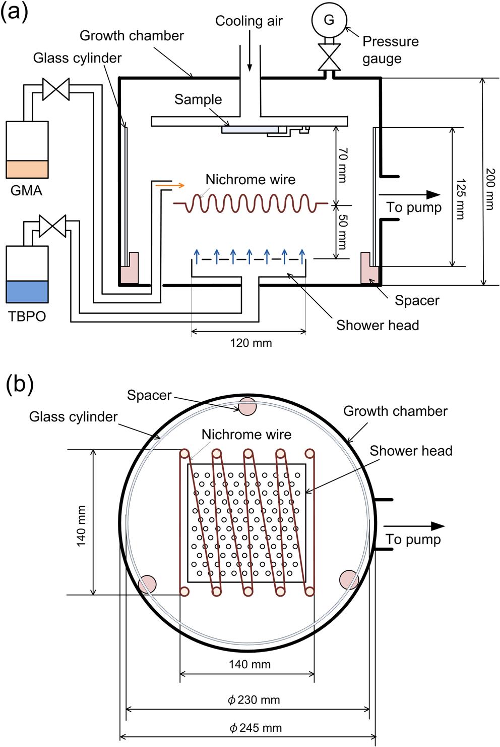
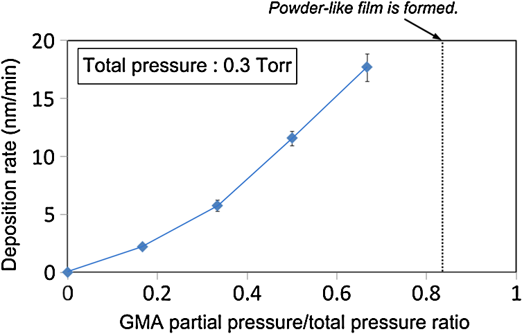
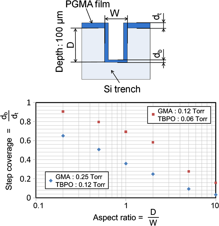
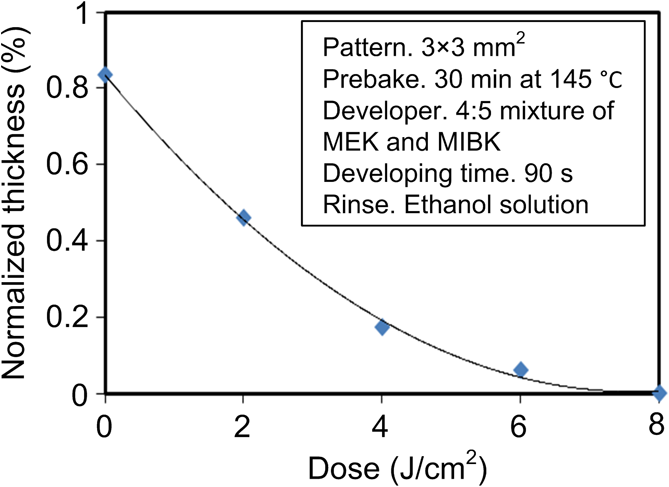
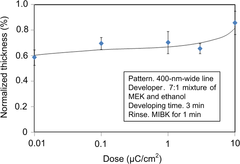
1.IntroductionRecently, in the research on microelectromechanical systems (MEMS) device fabrication, photo and electron-beam (EB) lithography technologies on a non-planar surface have been required for various applications. For instance, photolithography demonstrations of an optical fiber end,1 a vertical side wall for high-density packaging,2 and a cylindrical surface to fabricate a coil on a medical catheter3 have been reported. In the case of EB lithography, resist patterning on curved surfaces is required to fabricate a mold of a functional lens with an antireflection sub-wavelength structure4,5 or a diffraction grating.6,7 Thus, the technology of conformally coating resists on three-dimensional structures has become important for many applications. Thus far, the development of spray coating has provided one solution to achieve conformal coating on non-planar surfaces.8–12 This technology can provide relatively more uniform resist coatings on non-planar surfaces when compared with those realized with spin coating. However, even in the case of spray coating, uniform coatings are difficult to obtain because the flowing effect of the resists in the liquid phase process is not solved in principle. In particular, it is very difficult to uniformly coat resists onto a deep trench without breakage of the resist film at the corners and without preventing the formation of resist puddles at the bottom of the trench. In addition, this technology requires severe optimization of many parameters such as work temperature, work scanning speed, scanning repeat count, and the distance between the spray nozzle and the work object, depending on the material and shape of the work. Consequently, chemical vapor deposition (CVD), which allows deposition of lithographic resists in a vacuum, has been studied as an alternative method to liquid-phase processes.13,14 The vacuum process can completely avoid surface tension effects that occur in the liquid phase. In addition, the magnitude of the mean free path of gas molecules in a vacuum is usually larger than the dimensions of the trench structures fabricated for MEMS applications; this makes it easy to transport a precursor for the deposition of a lithographic polymer to the bottom of the trench. Therefore, the CVD method is expected to easily achieve conformal coating of a resist film on MEMS devices when compared with that achieved by the conventional liquid-phase coating processes. In a previous study, organosilicon was deposited as a deep-ultraviolet (UV) resist by using plasma-enhanced CVD.13 In this method, a -like material is fabricated as an etching mask by exposure to deep-UV light, and subsequently, the resist are removed by HF treatment. However, the HF treatment often causes undesirable damage of materials such as metallic oxides and base metals. Thus, the range of application of this inorganic resist is fairly limited. Organic resists are preferable to inorganic resists for the fabrication process because organic resists can be removed selectively using an organic solvent or via plasma treatment. A previous study has reported that poly-methyl methacrylate as positive EB resist14 and poly-styrene as negative resist15 can be deposited by plasma polymerization deposition. However, plasma polymerization deposition causes undesirable side reactions such as cross-linking. As a result, the sensitivity of the polymers to EB tends to be reduced. Thus, the CVD method, which can form high-quality organic resist film without undesirable side reactions, is a promising alternative. In this study, we employ initiated chemical vapor deposition (i-CVD) for organic resist coating on a non-planar surface. The i-CVD method based on radical polymerization requires far lesser energy than conventional plasma deposition methods due to the utilization of a catalytic reaction in the deposition process.16,17 Thus, this method can provide low-temperature deposition of high-quality polymer films without any side reactions. Thus far, several kinds of polymers have been synthesized by i-CVD. For example, many studies have used i-CVD for polymerization studies of poly-alkyl acrylates,18 poly-trivinyltrimethoxycyclotrisiloxane,19 poly-perfluoroalkylethylmethacrylate,20 poly-glycidyl methacrylate (PGMA),21,22 etc. In this study, we select PGMA as the lithographic resist. Although the patternability of PGMA as a positive deep-UV resist23 and negative EB resist24 has been investigated previously, PGMA has thus far been synthesized by conventional polymerization processes in solution. In addition, there are few reports on the patternability investigation of PGMA synthesized by i-CVD.21 In this study, in order to investigate the application potency of PGMA via i-CVD for use as lithographic resist for MEMS device fabrication, we first investigate the appropriate deposition conditions required to form a smooth PGMA film. Subsequently, we investigate its conformability by depositing the films on a deep Si trench. Finally, the photo and EB patternabilities are evaluated by lithographic pattering experiments. 2.Deposition Experiment of PGMA Film Via i-CVDPGMA was synthesized from glycidyl methacrylate (GMA) and tert-butyl peroxide (TBPO), which were used as monomer and initiator, respectively, as shown in Fig. 1. Some kinds of initiators, such as perfluorooctane sulfonyl fluoride, triethylamine, and TBPO have been studied for application in the i-CVD process.17 One of the advantages of using TBPO is that it can be decomposed homolytically by low-temperature heating using a hot catalytic wire. Its chemical stability and relatively high vapor pressure are also suitable for the CVD process. Thus, for the abovementioned reasons, we employed TBPO as the initiator in this study. The laboratory-fashioned i-CVD setup shown in Fig. 2 was used for deposition of the PGMA film. The deposition procedure used in the study is given below. At first, a Si sample substrate was positioned on a substrate holder in the chamber. Subsequently, the chamber was evacuated until the vacuum pressure was reduced to less than . Next, GMA and TBPO vapors were introduced into the chamber under reduced pressure. In order to increase the vapor pressure of GMA, the GMA storage bottle was heated to approximately 70 °C. The supplied amounts of TBPO and GMA were controlled by modulating the ratio of each partial pressure. Subsequently, a nichrome wire was heated by applying a current of 1.3 A to generate the radical initiator derived from TBPO. The temperature of the wire was measured as approximately 280 °C by using a thermocouple. The generated radical initiator on the wire surface caused generation of the GMA radical by collision between the radical initiator and the GMA monomer, which resulted in the initiation of radical polymerization of PGMA in the gas phase and on the sample surface. As a result, a PGMA film was formed on the sample surface. In the laboratory setup, a glass cylinder was placed in the chamber, and a narrow gap was provided between the cylinder and the wall of the chamber to decrease the exhaust rate of the gas molecules. As a result, the stay time of the initiator and precursor around the sample and the nichrome wire could be increased, and this resulted in the improvement of the uniformity of the deposited film. Fig. 1Synthesis of poly-glycidyl methacrylate (PGMA) via initiated chemical vapor deposition (i-CVD). 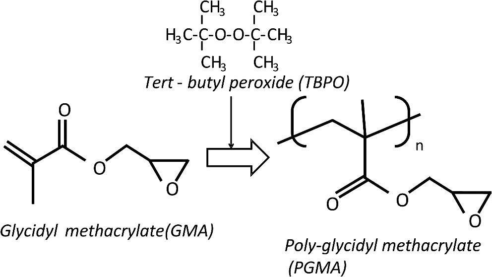 First, we investigated the optimum deposition conditions along with the deposition rate required to form a smooth PGMA film. The morphology of the film was investigated by atomic force microscopy (AFM). Figure 3(a) shows the AFM image of the PGMA film that was deposited for 30 min under a total pressure of 0.3 Torr at the GMA partial pressure/total pressure ratio of 0.33. It can be observed that the resulting PGMA film exhibits a very smooth surface. The film’s surface roughness (Ra) was measured to be approximately 1.2 nm by means of AFM. Figure 3(b) shows the image of the film deposited for 30 min at a GMA partial pressure/total pressure ratio of 0.83. Under this condition, a powder-like film was formed with large particles of diameter of approximately 3 μm. We speculate that the formation of the powder-like film was caused by increase in the collision probability of GMA molecules in the vapor phase due to high GMA concentration. This increase may have led to acceleration of the particle growth of PGMA not on the substrate surface but in the gas phase. As a result, the deposited film showed powder-like characteristics. Fig. 3Atomic force microscopy (AFM) images of PGMA films deposited at GMA partial pressure/total pressure ratios of (a) 0.33 and (b) 0.83. The total pressure in both deposition experiments was 0.3 Torr. The term Ra indicates the average and standard deviation of the arithmetic mean deviations of the profiles. 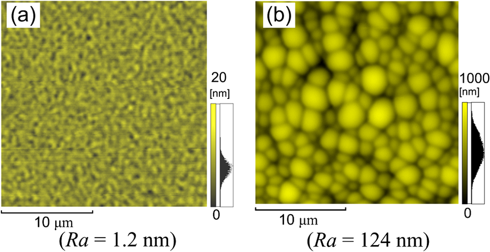 Figure 4 shows the relationship between the GMA partial pressure/total pressure ratio and the deposition rate of PGMA. This deposition experiment was also conducted at a total pressure of 0.3 Torr. As the GMA partial pressure ratio increased, the deposition rate also increased. This result was caused due to increase in the monomer supply. For cases in which the GMA partial pressure/total pressure ratio was less than approximately 0.7, all the deposited film samples exhibited very smooth surfaces without the presence of any particles. Figure 5 shows the relationship between the total pressure with a constant ratio of GMA to TBPO and the deposition rate. It can be observed that the deposition rate increased as the total pressure increased; this was attributed to increase in the monomer and initiator supplies. In this experiment, all deposited films exhibited smooth surfaces on the nanometer scale. Fig. 5Relationship between total pressure with constant ratio of GMA to TBPO and deposition rate of PGMA. 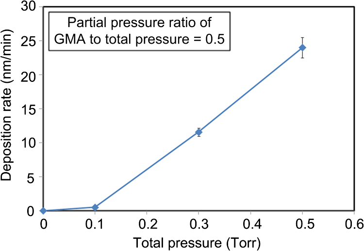 Thus, the deposition experiments confirm that the GMA partial pressure/total pressure ratio is one of the critical factors to be considered in order to obtain smooth PGMA films. When the GMA partial pressure was too large, the formation of powder-like films was observed. Thus, we demonstrated that smooth PGMA films can be formed by i-CVD on a Si substrate surface under appropriate deposition conditions. 3.Conformability Evaluation of PGMA Deposition Via i-CVDIn order to evaluate the conformability of PGMA deposition via the i-CVD method, the PGMA film was deposited on a Si trench. A Si trench with a depth of approximately 100 μm was fabricated by means of conventional deep reactive-ion etching. Subsequently, we conducted our deposition experiment on the trench. Figure 6(a) shows the cross-sectional scanning electron micrographs (SEMs) of the trench with an aspect ratio (AR) of 1 after PGMA deposition. This deposition experiment was conducted with GMA and TBPO partial pressures of 0.12 and 0.06 Torr, respectively. As seen from the figure, the surfaces of the top, bottom, and side walls could be conformally coated with the PGMA film without disconnections at the corners and scallop of the trench structure. For this deposition condition, the thicknesses of the film at the top and bottom sides were approximately 750 nm and 520 nm, respectively. Figure 6(b) shows the SEM of the trench with an AR of 5. In this case, the film thicknesses at the top and bottom sides measured 730 nm and 200 nm, respectively. The bottom-side thickness for an AR of 5 was less than that for an AR of 1. Figure 7 shows the relationship between the AR of the trench and the step coverage. The step coverage is defined as the ratio of the film thickness at the bottom to the thickness at the top. We found that the step coverage under low-pressure deposition conditions was better than that under conditions of high-pressure deposition. This result is reasonable because the gas-phase monomer is easily diffused into the Si trench under low pressure when compared with diffusion under high pressure due to increase in the mean free path of the gas molecules. Furthermore, it can be observed that the step coverage decreased as the AR of the Si trench increased. However, no disconnection of the PGMA film could be confirmed by microscope observations even if the AR reached 10. Therefore, i-CVD can be used to conformally coat a PGMA film onto three-dimensional structures such as trenches. 4.Patternability Evaluation of PGMA Film Deposited by i-CVD for Deep-UV LithographyIn order to evaluate the photo-patternability of the PGMA film deposited via i-CVD, we conducted a photolithography experiment, which is described below. First, the UV absorption characteristics of the PGMA film deposited via i-CVD were measured to determine the photosensitive wavelength. In this experiment, a thin PGMA film was deposited by i-CVD on a quartz-glass substrate. A conventionally polymerized PGMA film was also prepared by the spin-coating process using methyl ethyl ketone (MEK) solution of PGMA (purchased from Sigma-Aldrich Corporation) for comparison. Subsequently, the UV absorption spectra of both films were obtained using transmission measurements, as shown in Fig. 8. These spectra were nearly identical. It is to be noted that the wave undulation above 240 nm in Fig. 8(a) is probably generated from interference of UV light due to multi-reflections. In each spectrum, strong absorption below 240 nm along with a characteristic peak at a wavelength of approximately 215 nm could be observed. This absorption is attributed to the carbon backbone of the carbonyl group present in PGMA.23 This result indicates that i-CVD can provide PGMA films with optical properties identical to those of conventionally polymerized PGMA films used as deep-UV resists. In addition, the effective wavelength region contributing to PGMA photolithography was observed to be less than approximately 240 nm. Thus, the PGMA film deposited via i-CVD can potentially be used for deep-UV lithography applications. Fig. 8UV absorption spectra of (a) PGMA film deposited via i-CVD and (b) conventionally polymerized PGMA film. 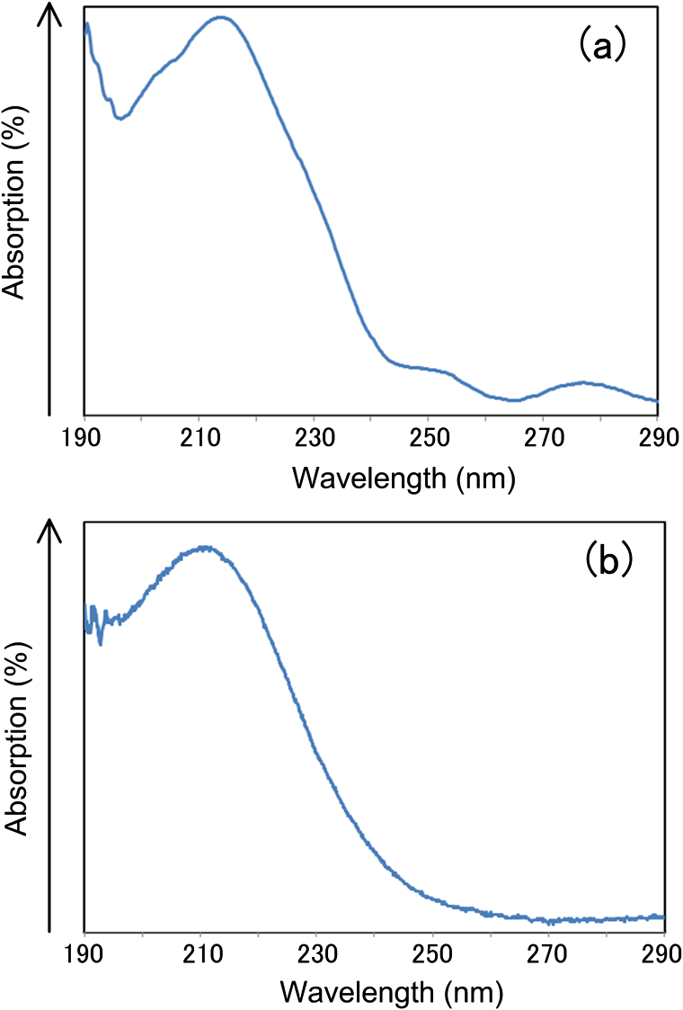 Subsequently, we examined the sensitivity curve of the PGMA film to deep-UV light. A 1-μm-thick PGMA film was deposited on a Si wafer with GMA and TBPO partial pressures of 0.25 and 0.12 Torr, respectively. After the sample was baked in an oven at 145 °C for 30 min, the film was exposed to 220-nm-wavelength deep-UV light obtained from a metal halide lamp through a chrome quartz photomask. The exposure area was set to be a square of dimensions of . Subsequently, the sample was developed by being immersed for in a mixture of MEK and methyl isobutyl ketone (MIBK). Finally, the sample was rinsed with ethanol solution and dried. Figure 9 shows the dose sensitivity curve of the PGMA film exposed to deep-UV light. The critical dose as evaluated from the result was found to be approximately . Further, we found that the contrast in this case was relatively low when compared with those of other conventional photoresists. In general, as the molecular weight distribution of a photoresist decreases, the contrast increases. Thus, we speculate that the molecular weight distribution of the PGMA film formed via i-CVD was relatively large when compared with that of chemically polymerized PGMA. Next, line-and-space () patterns were fabricated onto a 1.2-μm-thick film to investigate the patterning resolution. The patterning experiment was performed under exposure and development conditions identical to those for the measurement experiment of the sensitivity curve. Figure 10 shows the optical microscopy image of the 20-μm pattern and its surface profile. It is observed that a clear pattern was successfully fabricated by deep-UV lithography. The height of the pattern was measured to be approximately 1 μm, and this value was consistent with that obtained from the dose sensitivity curve. Figure 11 shows the image of a 10-μm pattern and its surface profile. In this case, although the height of the resist pattern decreased due to proximity effects and low contrast, an pattern could be fabricated fairly accurately. Fig. 10(Left) 20-μm line-and-space () patterns on PGMA film as defined by deep-UV lithography. (Right) Surface profile of line pattern. 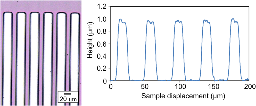 Fig. 11(Left) 10-μm pattern on PGMA film as defined by deep-UV lithography. (Right) Surface profile of line pattern.  Thus, PGMA films deposited via i-CVD can be employed as photoresists for deep-UV lithography. The pattern resolution of the 1.2-μm-thick PGMA film without considerable reduction of the film thickness was evaluated to be 20 μm. In these experiments, the deep-UV light used for exposure was not collimated. In addition, the development conditions were also not optimized. Therefore, we expect that the pattern resolution of the PGMA film can be further improved by using collimated deep-UV light along with optimization of the development process. 5.Patternability Evaluation of PGMA Film in EB LithographyFinally, we investigated the patternability of PGMA films in EB lithography. In this experiment, a 250-nm-thick PGMA film was deposited on a Si substrate under deposition conditions identical to those of the deep-UV lithographic experiment. In the measurement experiment of the sensitivity to EB, a 400-nm-wide line pattern was drawn using an EB with an acceleration voltage of 20 kV. Subsequent to the drawing of the pattern, the substrate was developed by being immersed for 3 min in a mixture of MEK and ethanol solution. The sample was finally rinsed with MIBK for 1 min and dried. The thickness evaluation and the observation of the patterned structure were conducted by AFM. Figure 12 shows the sensitivity curve of the PGMA film to EB. The figure indicates that low dose amounts of no more than were sufficient to achieve the required pattern definition. In this experiment, the dose could not be decreased to less than due to limitations in the EB drawing apparatus. Thus, the least dose amount for patterning was not measured but presumed to be less than . When compared to results of a previous report,24 the sensitivity of the PGMA film via i-CVD in this study was remarkably high. The reason for this increased sensitivity is unclear. However, we hypothesize that the PGMA film had a very large molecular weight. In general, the sensitivity of a negative-type EB resist increases as the molecular weight increases. It has been reported that the least dose amount required for a chemically-synthesized-PGMA resist with a molecular weight of 125,000 was measured to be approximately .24 Thus, we believe that the PGMA synthesized by i-CVD in our study may have had a large molecular weight of more than 200,000. Subsequently, we investigated the patterning resolution of PGMA film via the pattern definition experiment. In this experiment, a 250-nm-thick PGMA film deposited on a Si substrate was used as the patterning sample. Figure 13 shows the AFM image of the 350-nm pattern defined by EB lithography using a dose of and its surface profile. A fine pattern was successfully defined in the experiment. The difference of the average height between the exposed and unexposed areas measured approximately 120 nm. This pattern height is considered to be the acceptable margin for microfabrication processes. In the case of the 150-nm pattern, as shown in Fig. 14, although the difference of the average height between the exposed and unexposed areas decreased and varied depending on the position of height measurement, the required patterning could be successfully realized. Fig. 13(Left) AFM image of 350-nm pattern defined by EB lithography. (Right) Surface profile of the line pattern along the A-A’ line indicated in the left image. 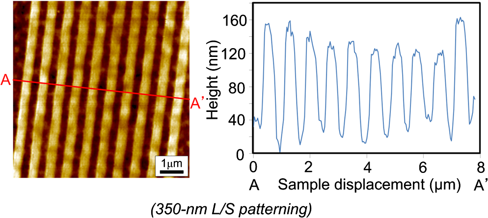 Fig. 14(Left) AFM image of 150-nm pattern defined by EB lithography. (Right) Surface profile of the line pattern along the B-B’ line indicated in the left image. 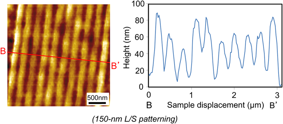 Therefore, PGMA films deposited via i-CVD can be employed as highly sensitive resists for EB lithography. Further, we believe that pattern resolution with EB lithography can be improved by optimization of the development conditions. 6.ConclusionIn this study, we investigated the potential applicability of PGMA films formed via i-CVD as lithographic resists for microfabrication of non-planar structures. From our deposition experiments, we found that the GMA partial pressure/total pressure ratio is one of the critical factors to be considered in obtaining smooth PGMA films. Further, smooth PGMA films can be formed by i-CVD under appropriate pressure conditions. The results of our deposition experiments on a Si trench demonstrated that i-CVD can effectively enable conformal coating of polymer films on a three-dimensional structure such as a deep trench with a high AR. When PGMA film is used as a mask for dry etching process in actual MEMS device fabrication, the film-thickness difference between the top and bottom of the trench might not be optimal if the etching resistance of the film to plasma is low. However, the deposited film may be practically useful as a mask for the wet etching process of a metal by its etchant or the etching of by HF solution. The optimization of the deposition conditions can further improve the step coverage. For example, increase in the substrate temperature is considered to be effective in improving the step coverage; the temperature increase can enhance surface diffusion on the substrate surface. In both deep-UV and EB lithography experiments, we successfully demonstrated the patterning of PGMA film samples. In deep-UV lithography, a fine 20-μm pattern with a pattern height of 1 μm could be defined. This resolution is considered to be suitable for MEMS device fabrication. In EB lithography, a fine 350-nm pattern with a pattern height of 120 nm was fabricated. In addition, the PGMA film deposited via i-CVD exhibited remarkably high sensitivity; the lowest dose amount for patterning was evaluated to be less than . In general, it is very difficult to form such a sensitive EB resist by plasma polymerization. Thus, i-CVD can be used to form EB resist films with higher sensitivity than those obtained using plasma polymerization. We believe that the i-CVD process has great potential to be applied as the coating technology of lithographic resists on three-dimensional structures in the fabrication of MEMS devices. AcknowledgmentsThis work was supported in part by a Grant-in Aid for Scientific Research from the Japanese Ministry of Education, Culture, Sports, Science and Technology. This work was also supported by World Premier International Research Center Initiative (WPI Initiative), MEXT, Japan and the Formation of Innovation Center for Fusion of Advanced Technologies. ReferencesM. Sasakiet al.,
“Direct photolithography on optical fiber end,”
Jpn. J. Appl. Phys., 41
(6B), 4350
–4355
(2002). http://dx.doi.org/10.1143/JJAP.41.4350 JJAPA5 0021-4922 Google Scholar
H. Moriiet al.,
“Proposal of high-density packaging construction and conductive pattern forming method on vertical wall using spray coating technology,”
IEEJ Trans. Sens. Micromach., 131
(1), 40
–44
(2011). http://dx.doi.org/10.1541/ieejsmas.131.40 1341-8939 Google Scholar
T. Matsunagaet al.,
“A High-resolution endoscope of small diameter using electromagnetically vibration of single fiber,”
IEEJ Trans. Sens. Micromach., 129
(11), 399
–404
(2009). http://dx.doi.org/10.1541/ieejsmas.129.399 1341-8939 Google Scholar
Y. KanamoriE. RoyY. Chen,
“Antireflection sub-wavelength gratings fabricated by spin-coating replication,”
Micro. Eng., 78–79 287
–293
(2005). http://dx.doi.org/10.1016/j.mee.2004.12.039 MIENEF 0167-9317 Google Scholar
C. J.-F. KuoH.-M. TuT.-L. Su,
“Optimization of the electron-beam-lithography parameters for the moth-eye effects of an antireflection matrix structure,”
J. Appl. Polym. Sci., 102
(6), 5303
–5313
(2006). http://dx.doi.org/10.1002/(ISSN)1097-4628 JAPNAB 1097-4628 Google Scholar
O. Masudaet al.,
“The fabrication of optical element molds through the use of electron beam lithography,”
Konica Minolta Technol. Rep., 1 31
–34
(2004). Google Scholar
S. OgataM. TadaM. Yoneda,
“Electron-beam writing system and its application to large and high-density diffractive optic elements,”
Appl. Optic., 33
(10), 2032
–2038
(1994). http://dx.doi.org/10.1364/AO.33.002032 APOPAI 0003-6935 Google Scholar
S. Aoyagiet al.,
“Fabrication of MOSFET capacitive sensor using spray coating method,”
IEEJ Trans. Sens. Micromach., 127
(3), 153
–159
(2007). http://dx.doi.org/10.1541/ieejsmas.127.153 1341-8939 Google Scholar
M. Ishizukaet al.,
“Metallization on three dimensions microstructures using photoresist spray coating for microdirect methanol fuel cell,”
Jpn. J. Appl. Phys., 45
(10A), 7944
–7948
(2006). http://dx.doi.org/10.1143/JJAP.45.7944 JJAPA5 0021-4922 Google Scholar
T. IkeharaR. Maeda,
“Fabrication of an accurately vertical sidewall for optical switch applications using deep RIE and photoresist spray coating,”
Microsyst. Technol., 12
(1–2), 98
–103
(2005). http://dx.doi.org/10.1007/s00542-005-0008-8 0946-7076 Google Scholar
V. K. Singhet al.,
“Deposition of thin and uniform photoresist on three-dimensional structures using fast flow in spray coating,”
J. Micromech. Microeng., 15
(12), 2339
–2345
(2005). http://dx.doi.org/10.1088/0960-1317/15/12/016 JMMIEZ 0960-1317 Google Scholar
N. P. PhamJ. N. BurghartzP. M. Sarro,
“Spray coating of photoresist for pattern transfer on high topography surfaces,”
J. Micromech. Microeng., 15
(4), 691
–697
(2005). http://dx.doi.org/10.1088/0960-1317/15/4/003 JMMIEZ 0960-1317 Google Scholar
M. W. HornS. W. PangM. Rothschild,
“Plasma-deposited organosilicon thin films as dry resists for ultraviolet lithography,”
J. Vac. Sci. Technol. B, 8
(6), 1493
–1496
(1990). http://dx.doi.org/10.1116/1.585103 JVTBD9 0734-211X Google Scholar
S. Moritaet al.,
“Plasma polymerized methylmethacrylate as an electron-beam resist,”
J. Appl. Phys., 51
(7), 3938
–3941
(1980). http://dx.doi.org/10.1063/1.328170 JAPIAU 0021-8979 Google Scholar
F.-O. Fonget al.,
“Plasma polymerized styrene: a negative resist,”
J. Vac. Sci. Technol. B, 6
(1), 375
–378
(1988). http://dx.doi.org/10.1116/1.584002 JVTBD9 0734-211X Google Scholar
R. SreenivasanK. K. Gleason,
“Overview of strategies for the CVD of organic films and functional polymer layers,”
Chem. Vap. Deposition, 15
(4–6), 77
–90
(2009). http://dx.doi.org/10.1002/cvde.v15:4/6 CVDEFX 0948-1907 Google Scholar
W. E. TenhaeffK. K. Gleason,
“Initiated and oxidative chemical vapor deposition of polymeric thin films: iCVD and oCVD,”
Adv. Funct. Mater., 18
(7), 979
–992
(2008). http://dx.doi.org/10.1002/(ISSN)1616-3028 AFMDC6 1616-3028 Google Scholar
K. K. S. LauK. K. Gleason,
“Initiated chemical vapor deposition (iCVD) of poly(alkyl acrylates): an experimental study,”
Macromolecules, 39
(10), 3688
–3694
(2006). http://dx.doi.org/10.1021/ma0601619 MAMOBX 0024-9297 Google Scholar
W. S. O’ShaughnessyM. GaoK. K. Gleason,
“Initiated chemical vapor deposition of trivinyltrimethylcyclotrisiloxane for biomaterial coatings,”
Langmuir, 22
(16), 7021
–7026
(2006). http://dx.doi.org/10.1021/la0607858 LANGD5 0743-7463 Google Scholar
M. Maet al.,
“Superhydrophobic fabrics produced by electrospinning and chemical vapor deposition,”
Macromolecules, 38
(23), 9742
–9748
(2005). http://dx.doi.org/10.1021/ma0511189 MAMOBX 0024-9297 Google Scholar
Y. Maoet al.,
“Towards all-dry lithography: electron-beam patternable poly(glycidyl methacrylate) thin films from hot filament chemical vapor deposition,”
J. Vac. Sci. Technol. B, 22
(5), 2473
–2478
(2004). http://dx.doi.org/10.1116/1.1800351 JVTBD9 0734-211X Google Scholar
Y. MaoK. K. Gleason,
“Hot filament chemical vapor deposition of poly(glycidyl methacrylate) thin films using tert-butyl peroxide as an initiator,”
Langmuir, 20
(6), 2484
–2488
(2004). http://dx.doi.org/10.1021/la0359427 LANGD5 0743-7463 Google Scholar
Y. Mimuraet al.,
“Deep-UV photolithography,”
Jpn. J. Appl. Phys., 17
(3), 541
–550
(1978). http://dx.doi.org/10.1143/JJAP.17.541 JJAPA5 0021-4922 Google Scholar
Y. Taniguchiet al.,
“PGMA as a high resolution, high sensitivity negative electron beam resist,”
Jpn. J. Appl. Phys., 18
(6), 1143
–1148
(1979). http://dx.doi.org/10.1143/JJAP.18.1143 JJAPA5 0021-4922 Google Scholar
Biography |