|
|
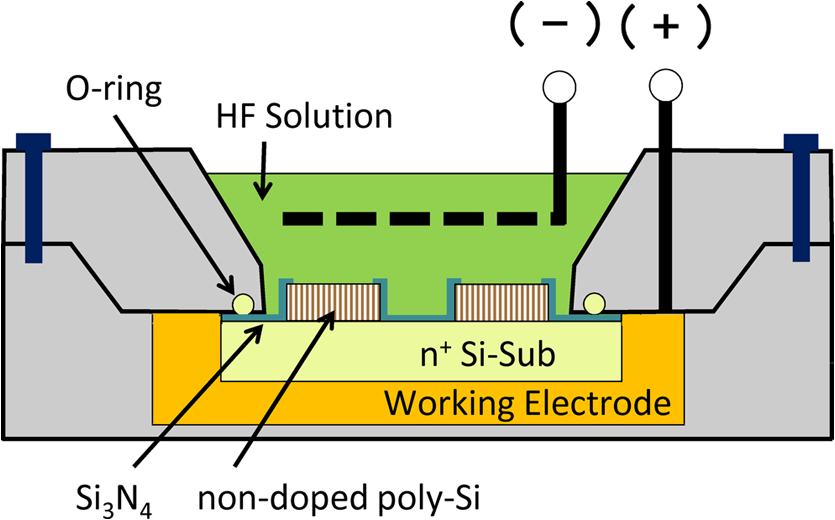
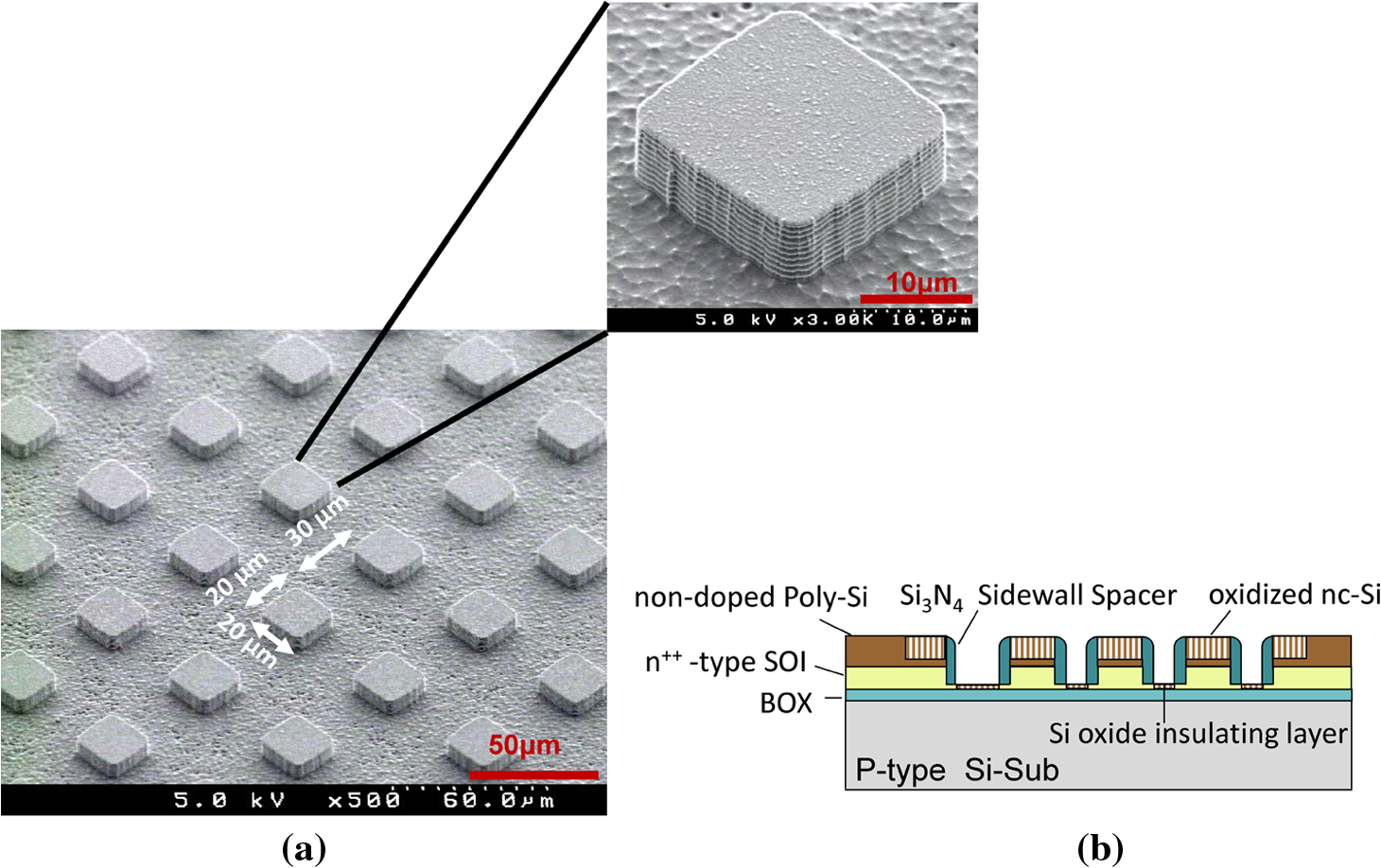
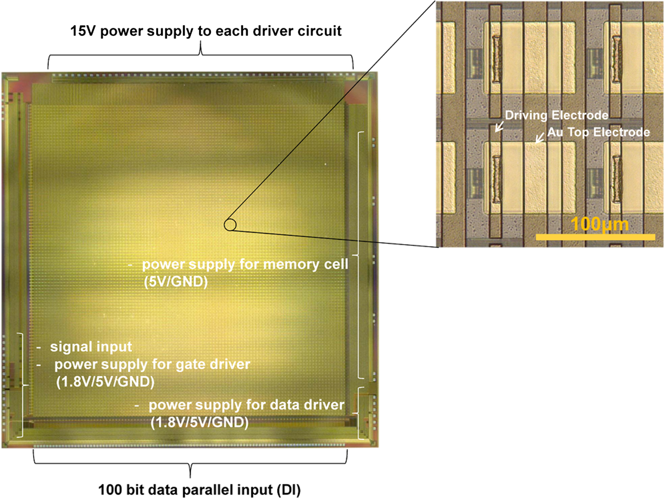
1.IntroductionNanoscale lithographic technologies have been intensely studied for the next generation of semiconductor manufacturing. Maskless/direct-write electron-beam (e-beam) lithography is a candidate for the upcoming 16-nm node and beyond. It compares well with projection technologies such as a combination of 193 nm immersion lithography and self-aligned spacer double patterning and/or extreme ultraviolet (EUV) lithography. At present, however, a direct-write e-beam system remains challenging as far as achieving an acceptable throughput for mass production goes; i.e., a throughput improvement of more than three orders of magnitude will be required for commercial semiconductor/micro electro mechanical system (MEMS) fabrication. Massive parallelism has been suggested as a potential way around this roadblock,1 and many innovative concepts in multiple e-beam imaging have been proposed and are being developed.2–8 If a commercial level of throughput can be achieved, this technology can potentially reduce the cost of manufacturing photomasks for the next generation of ultra-large-scale integrated circuit (ULSI) devices, as well. In addition, it could enable a timely response for making diversified photomasks for MEMS devices made in high-mix, low-volume production. These potential industrial advantages prompted us to begin development of a massively parallel direct-write e-beam system with a throughput comparable to that of existing optical steppers. The expected throughput using a system described in Sec. 2.1 could be 10 to 100 wafers (300 mm in diameter) per hour, depending on the switching speed, data transfer rate, and electron beam current density. The electron source used in this system is a nanocrystalline Si (nc-Si) ballistic surface electron emitter,9,10 in which a projection of the electron beam can resolve patterns 30 nm in width.11 An array of microminiaturized nc-Si electron emitters are integrated with an active-matrix driving large-scale integrated circuit (LSI), and the beamlets exposing pixels in parallel are operated at a CMOS-compatible voltage. This paper presents our prototype nc-Si electron emitter array compatible with the active-matrix driving LSI, and it discusses an experimental evaluation of the performance of an electron source for massively parallel exposure. 2.Basic Concept of the System2.1.System ConfigurationThe whole system embodies an array of microcolumns, each having an nc-Si electron emitter array in combination with microminiaturized electron optical elements for projecting a reduced image () of focused e-beams. The microcolumns have very small physical dimensions, and they are made by utilizing MEMS fabrication technology. The result is a compact overall mechanical system with substantial cost benefits. Figure 1 shows the configuration of the miniaturized column consisting of the active matrix nc-Si electron emitter array, an array of condenser lenses, anode plates, a rotation coil, telecentric reduction lenses, deflectors, and collection optics providing functions of dynamic focusing, alignment collection, and deceleration. Also embedded are metrology systems, i.e., a stigmator for astigmatism correction and a Faraday cup for real-time monitoring of the projected pixel images. Fig. 1Configuration of the miniaturized column having an active-matrix nc-Si electron emitter array in combination with microminiaturized electron optical elements. 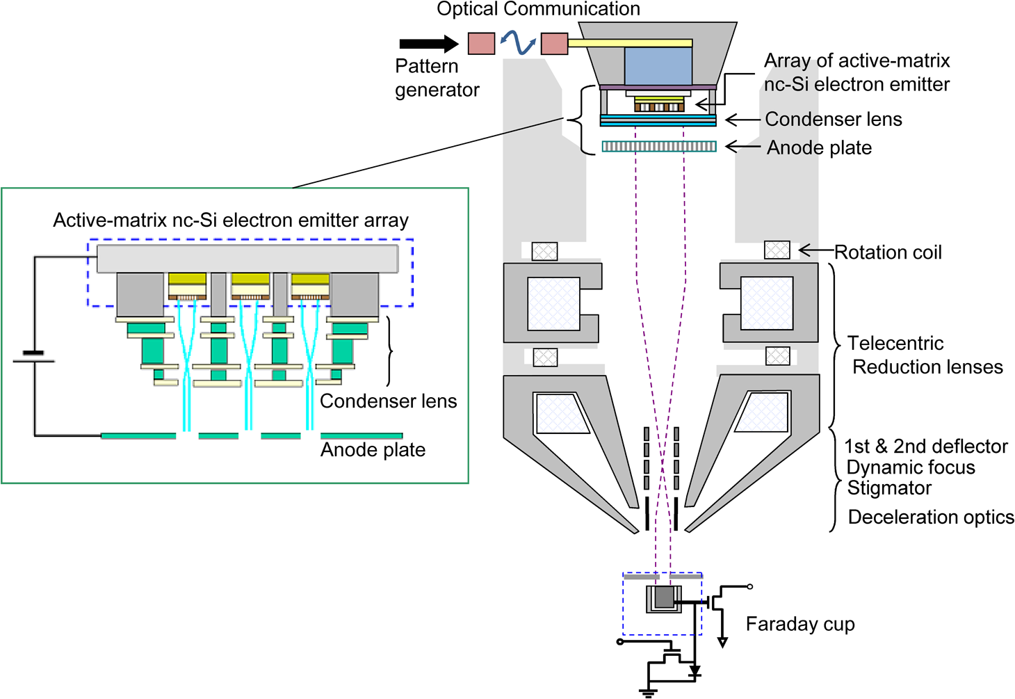 The nc-Si emitters are arranged in a pixels array with a pitch size of 10 μm. The array covers an area of and is integrated with the active-matrix driving LSI. The one million beamlets projecting pixels simultaneously are switched on and off by changing the CMOS-compatible voltage. The constitutive array of condenser lenses consists of a grid of electrostatic Einzel-type lenslets, which collimate the emitted electron beams from the emitter. The array of lenslets is separately fabricated and mechanically bonded onto the array of nc-Si emitters (see Fig. 1). The bonding process is currently under development in which each is aligned in a one-to-one manner with the required accuracy of a submicrometer by using a piezo-actuated manipulator under in-situ scanning electron microscope (SEM) observation of the fabricated alignment marks. Fabrication of monolithically integrated lenslets with the array of nc-Si emitters are also being studied in parallel. The nc-Si emitter exhibits favorable emission properties in terms of its perpendicularity (i.e., lower emission angle) and uniformity over the whole surface,12 originating from the ballistic transfer of electrons passing through the nanosilicon-wired-array structures. This feature allows the condenser lenses to be easily designed so as to collimate and focus the emitted electrons, leading to reduced beam size () and increased current density () for each electron beam without any change in pitch size (10 μm). Each of the electron beamlets passing through the array of condenser lenses is accelerated at the anode plate through apertures with an acceleration voltage of . The beamlets then enter a telecentric reduction lenses consisting of two electromagnetic lenses. Here, they are focused to project a reduced image onto the wafer. The two embedded deflectors scan the focused beamlets to perform the direct-write operation in synchronization with the controlled motion of the stage. 2.2.Compensation of Chromatic and Spherical AberrationsSince a general rotationally symmetric lens system cannot make a concave lens creating a negative aberration, neither chromatic nor spherical aberration can be compensated by optimizing the configuration of the electric and magnetic fields in the electron optics presented in Fig. 1. Chromatic aberration is inherently generated by the energy dispersion of the emitted electrons, and this restricts the practical resolution of the system. Our previous study demonstrates that the initial energy dispersion of emitted electrons from an nc-Si ballistic emitter is innately small (approximately 2 eV at RT and 500 meV at 100 K),11,13,14 and thus, the chromatic aberration can be sufficiently optimized by making the energy distribution as close to monochromatic as possible. In this regard, we are improving the physical properties of nc-Si itself, as well as exploring other potential schemes such as operating the emitter at a lower temperature, which has been demonstrated to significantly reduce energy spread of the emitted electrons.11,13,14 On the other hand, spherical aberration should be compensated on a reduced image projected by the telecentric reduction lens system in order to improve the practical resolution. It can be corrected by controlling each of the driving voltages in the picture cells of the integrated LSI, so that the spatial distribution of the emitted beamlets’ energy can be adjusted to compensate for the spherical aberration and be balanced on the projected image. At present, we are studying how to incorporate such a function into the next design of the LSI. 3.Prototype of Nanocrystalline Silicon Emitter Array3.1.Evaluation of Emission Characteristics from Prototype Dot Pattern Array of nc-Si EmittersThe active-matrix electron emitter includes an array of nc-Si dot patterns, each connected electrically to through silicon via (TSV) plugs from the back side of the supportive substrate. The device consists of an aligned joint of the TSV plugs with driving pads on the active-matrix LSI. In prototyping this device, a test structure was preliminary fabricated to ascertain if the electron emissions from the array would work in practice; a 2-μm-thick nondoped columnar polycrystalline silicon (poly-Si) film was deposited on a 4-inch -type Si substrate, and the poly-Si was dry-etched with a photoresist mask to form an array of dots with a pitch of 50 μm, each dot having an area of μm2. After that, a 0.15-μm-thick film was deposited over the whole wafer surface by low-pressure chemical vapor deposition (LPCVD). Then, apertures were opened on the film with a photoresist mask at the top surfaces of the dots by highly selective reactive-ion-etching (RIE) of the film over the underlying poly-Si layer in a mixture of gas. After the individual poly-Si top surfaces were exposed, each was selectively anodized in a HF solution, which promoted preferential local dissolution at the poly-Si grain boundaries and resulted in structured porous silicon. Because of the columnar geometry of the poly-Si grains, the fabricated porous silicon includes nanodots with columnar/vertically arranged interconnections similar to nanometric wires (“nanowires”). The anodization was conducted as follows: The processed 4-inch wafer was diced into 12 pieces; each specimen measured and was grooved into a working electrode of a Teflon sample holder in contact with the backside surface. This was followed by mechanical screw-clamping of the top surface to seal the back surface from the solution (see Fig. 2). An anodic current was galvanostatically applied for 6 s to the working electrode in a solution of HF (55%): at a current density of under the irradiation of a tungsten lamp. After that, the sample was treated with rapid-thermal-oxidation (RTO) at 900°C in a dry ambient for 25 min to form a thin oxide layer surrounding each Si nanodot in the nanowire array. The surface was then treated with high pressure water vapor annealing (HWA) at 1.3 MPa and 260°C for 3 h and subsequent super critical rinse and dry (SCRD) in order to obtain sufficiently passivated nc- interfaces. The interfaces had an extremely low defect density, because of the minimized mechanical stress of the surrounding .15 Then, a () common electrode was selectively RF-sputtered by using a liftoff process with resist mask onto an area excluding the top surfaces of the dots. This was followed by depositing a () surface electrode over the whole surface. This two-step deposition process improves step coverage for each dot pattern, even for extremely thin surface electrodes. Figure 3(a) shows an SEM image of the fabricated test structure array consisting of a dots pattern of nc-Si emitters. The corresponding structure is schematically illustrated in Fig. 3(b). Fig. 3(a) SEM image of the fabricated test structure of a array of nc-Si emitters with a pitch of 50 μm, with each emitter having an area of μm2; (b) schematic illustration of the corresponding structure. 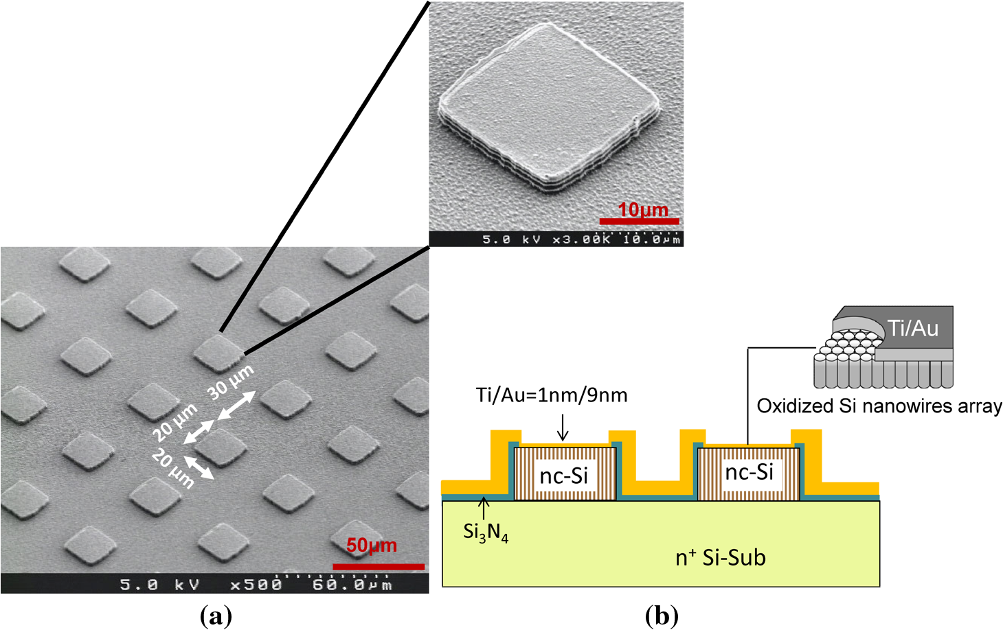 Figure 4(a) shows the characteristics of the diode current density and corresponding emission current density as a function of applied voltage obtained from the sample shown in Fig. 3. The measurement circuit is displayed in the upper part of the figure. The plot shows electron emissions from the emitter array at exceeding the work function of the Au electrode. The current density reached 10 μA/cm2 at 15 V, which corresponds to an amplified electron current density of passing through the integrated condenser lenslets () (see Fig. 1). Figure 4(b) is a Fowler-Nordheim (FN) plot obtained from the emission curve in Fig. 4(a). It should be noted that the linear behavior covered the whole range of applied voltage, although the emission exhibited variability in the low voltage region (), presumably due to a space charge effect of the emitted electrons with relatively low kinetic energy. The linearity of the FN plot suggests that electrons were ballistically transported via cascade tunneling through interconnected nanodots in the silicon nanowires. Fig. 4(a) Characteristics of diode current density and corresponding emission current density vs. applied voltage ; (b) Fowler-Nordheim plot obtained from Fig. 4(a). 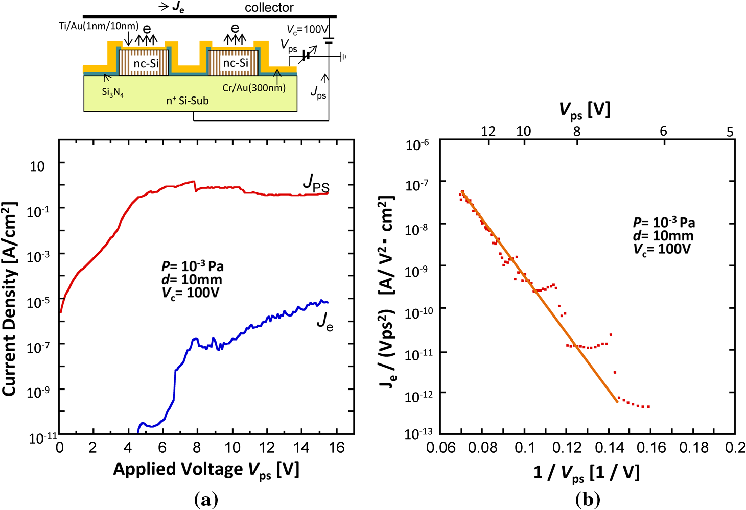 3.2.Fabrication of nc-Si Emitter Array on SOI Substrate for Integration with the Active-Matrix Driving LSInc-Si emitters were fabricated on SOI substrate with via-last processed TSV plugs connected to the array from the back side, with each plug and emitter forming an aligned joint with driving pads on the active-matrix LSI. The essential features of the fabrication process are illustrated in Fig. 5. As shown in this figure, a 2-μm-thick nondoped columnar poly-Si film is deposited on a 4-inch SOI wafer having an -type active layer (0.005 Ωcm). The active layer/poly-Si stacking structure with a photoresist mask is dry etched, until the underlying active layer on the BOX is 50 nm thick. The resulting array of dots covers an area of μm2 (steps 1-2). Next, RIE is used to conduct a highly selective sidewall-spacer etching of 0.15-μm-thick LP-CVD over the underlying active layer (step 3). After the wafer is diced into smaller specimens, these smaller specimens are anodized in a HF solution with the electrochemical cell shown in Fig. 2. Immediately after that, they are treated with under the same conditions described in Sec. 3.1 (step 4). Then, via-filled TSV plugs (steps 5 to 6), solder bonds with the active-matrix LSI through the Au–Sn bump structures (step 7), and electrodes (step 8) are formed. Fig. 5Schematic illustration of the fabrication process flow of an nc-Si emitter array integrated with active-matrix driving LSI. The nc-Si emitter array was fabricated on SOI substrate with via-last processed TSV plugs. 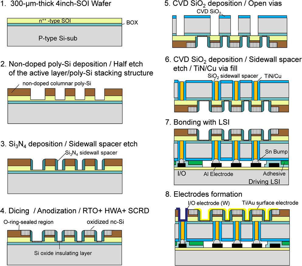 Galvanostatically anodizing the structure fabricated on an SOI substrate (step 4) leads to an extremely high potential due to the difficulty of injecting carriers through the BOX layer if the working electrode is connected only to the back of the sample. In fact, the potential reached several tens of volts when an anodic current was applied under the galvanostatic condition of ; such a situation is probably accompanied by an undesirable BOX breakdown process. Thus, during the anodization process in step 4, the working electrode was connected directly to the top surface, bypassing the remaining active layer in the upper part of the surrounding sidewall of the grooved substrate. The remaining active layer among the dots was dissolved and became porous and easily oxidized to form an insulating layer in the subsequent RTO treatment. This layer formed a self-aligned electrical separation among the dots, resulting in complete separation of the pixels. Nanostructures constituting the nc-Si cause the band gap to widen due to the quantum confinement effect.16 Experimentally exposing a YAG Laser (266 nm) on an anodized poly-Si surface on SOI substrate with subsequent treatments under the same conditions as described in step 4 led to red band photoluminescence (PL) with a peak intensity at a wavelength of (1.8 eV) (see Fig. 6). This indicates that Si nanowire array structures with a derived size of were formed.16 Electron emissions were also observed from this sample through a subsequently deposited () electrode on the top surface in association with applied voltage, demonstrating that the anodizing process is workable on an SOI substrate, as well as on Si. Fig. 6Photoluminescence (PL) spectra obtained from anodized nondoped ply-Si surfaces on SOI substrate with subsequent treatments of RTO and . 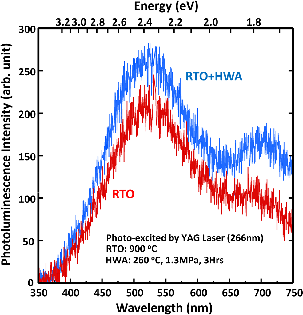 Figure 7(a) shows an SEM image of the structure just after step 4 in Fig. 5. The corresponding structure is schematically illustrated in Fig. 7(b). The anodizing process in step 4 could be conducted at a lower applied anodic-voltage () for galvanizing the . As shown in Fig. 7(a), a array of nc-Si emitters with a pitch of 50 μm, each having an area of μm2, was successfully formed on the SOI substrate. Cross-sectional SEM observation showed that the layer remaining among the dot patterns was sufficiently oxidized as an insulating layer, and the thickness was approximately 50 nm over the whole surface. 3.3.Advanced Fabrication Process for nc-Si Emitter ArrayThe results described in Secs 3.1 and 3.2 demonstrated that the array of microminiaturized nc-Si emitters worked in practice by emitting ballistic electrons and was manufacturable on an SOI substrate, thereby enabling us to integrate it with an active-matrix driving LSI. However, the fabrication process shown in Fig. 5 remains a challenge for processing larger wafers for mass production in terms of SOI usage related to cost benefit, as well as the manufacturability of the anodization process. Figure 8 shows an advanced structure and corresponding fabrication process flow to address these issues. Here, the nc-Si emitter array is fabricated on a Si substrate with via-first processed TSV plugs filled with an -type LP-CVD poly-Si film. All of the processes are done on 4-inch Si wafer, and they can be extended to larger wafer processes. Since most of the processes shown in Fig. 8 include many of the processes described in the previous section, only the essential features will be described here. Fig. 8Schematic illustration of the advanced process flow for fabricating an nc-Si emitter array integrated with active-matrix driving LSI. The nc-Si emitter is fabricated on Si substrate with via-first processed TSV plugs. 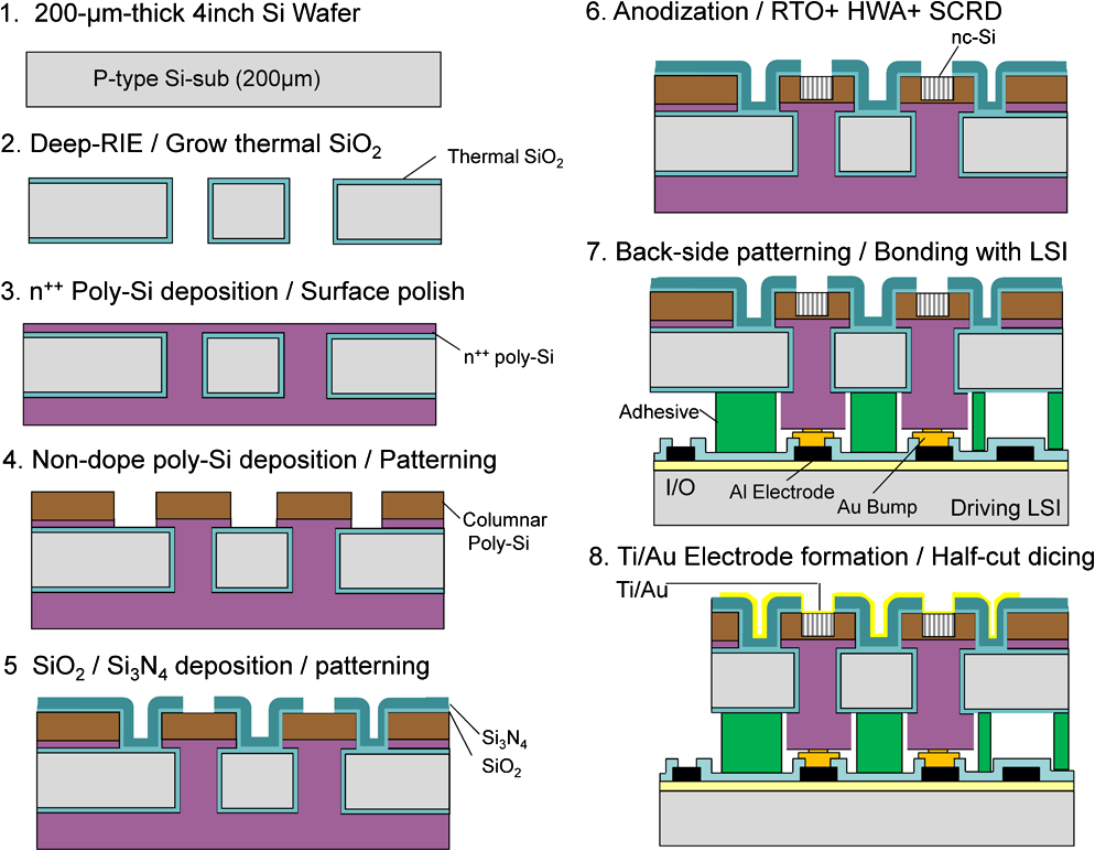 A 200-μm-thick 4-inch Si wafer (p-type, 5k Ωcm) is deep-reactive-ion-etched (Deep-RIE) with a photoresist mask to open through-silicon-vias (15 μm in diameter) with a pitch of 50 μm, and a thermally grown layer is formed over the whole surface (steps 1-2). Next, an -type LP-CVD poly-Si film is deposited over the whole surface to completely fill the vias, and both surfaces are chemical-mechanical polished (CMP) until the remaining -poly-Si thickness on one surface is thinner ( μm) than the thickness on the other surface (step 3). After that, a 2-μm-thick nondoped columnar poly-Si film is deposited on the thinner side, and a array of dots with a pitch of 50 μm (each dot having an area of μm2) is formed on the -poly-Si/nondoped poly-Si stack structure (step 4). Next, thermally grown film and LP-CVD film are deposited and patterned on the top surfaces of the dots (step 5). Subsequently, each exposed poly-Si surface is anodized by galvanostatically applying an anodic current from the back of the -poly-Si film (step 6). After treatment, the back side -poly-Si is patterned as an electrode, and an aligned joint with driving pads is formed on the active-matrix LSI through Au-Si eutectic bonding (step 7). Finally, a surface electrode is formed, and half-cut dicing is done to expose the bonding pads of the LSI (step 8). This advanced process yields not only cost benefits by using Si substrate instead of SOI, but also increased manufacturability for mass production in the anodization process by applying a uniform galvanostatic current to each dot from the back of the wafer through each filled via. 4.Design and Prototype of the Active-Matrix Driving LSIThis section presents our first prototype active-matrix LSI circuit, which is capable of simultaneously driving all pixels of the nc-Si electron emitter array in accordance with a bitmap image preliminarily stored in a built-in memory. The bitmap image is temporarily stored and sequentially output in conjunction with input data by switching the driving voltage on and off. The LSI consists of three circuit blocks: a data-line driver circuit, a gate line drive circuit, and a bit cell array with a 100-μm pixel pitch, with each cell having a two-bit memory and a driving electrode. The chip size is , including the largest circuit block of the bit cell array, which is . Figure 9(a) illustrates the signal operation of the prototype active-matrix LSI. The pattern layout of one bit cell is shown in Fig. 9(b). Figure 10 is the timing chart of the circuit, in which the minimum time value of the individual control signal, as confirmed by simulation, is displayed in the figure. Fig. 9(a) Signal operation of prototype active-matrix driving LSI; (b) pattern design of one cell of the circuit. 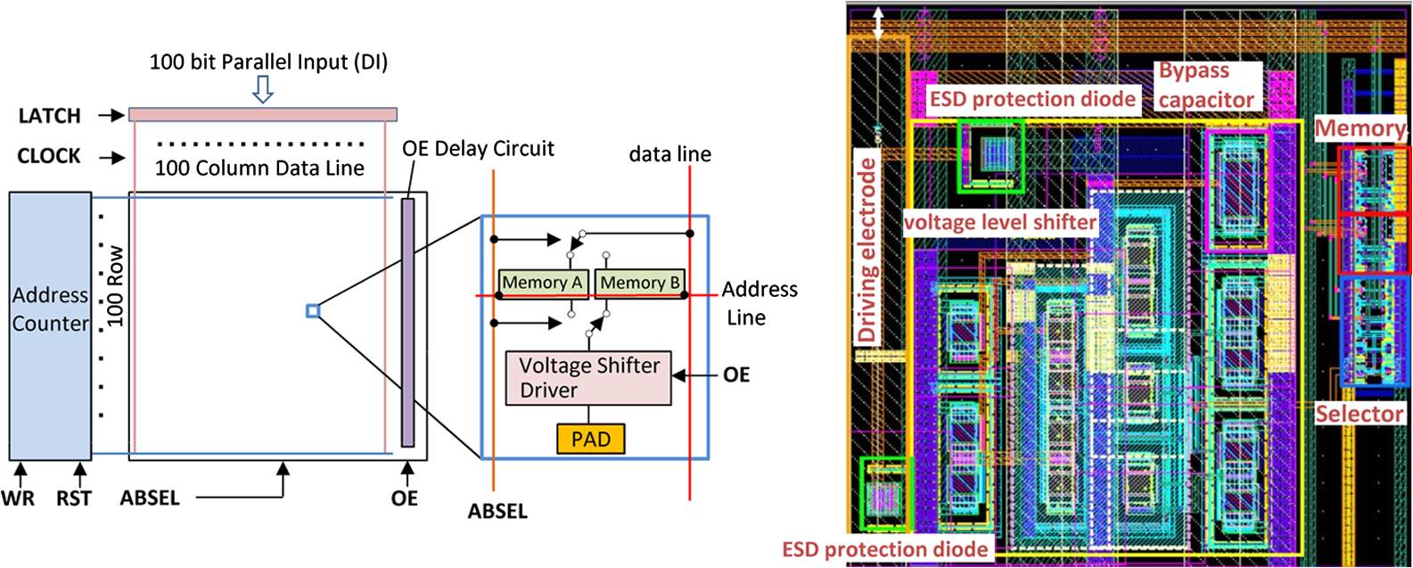 Fig. 10Timing chart of an active-matrix driving LSI. Each time displayed in the illustration indicates the minimum time of an individual control signal, as calculated by simulation. 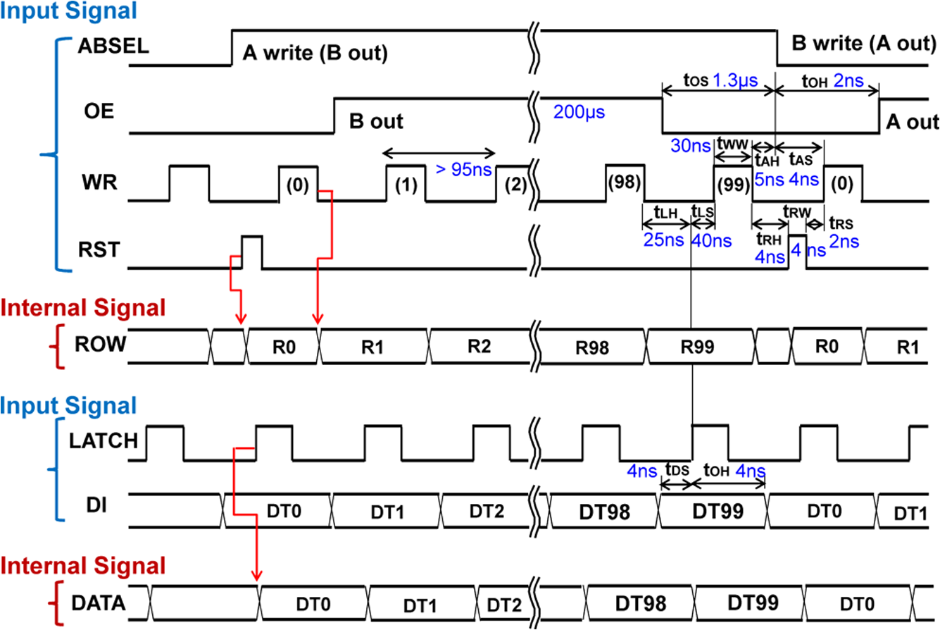 The boldface symbol names (LATCH, CLOCK, WR, RST, ABSEL, OE) in Fig. 9(a) represent input signals (see Fig. 10). DI represents 100-bit data externally input in parallel, which is subsequently latched by the LATCH signal input and stored in a 100-column data line as a set of row data by the data-line driver circuit, as shown in Fig. 9(a). Each row of data (100 bits) is sequentially written by the gate line drive circuit into a selected row address data line during a specific period of time given by ABSEL, RST, and WR signal inputs, resulting in writing of the pixels data into each memory of the bit cell array, as shown in Figs. 9(a) and 10. The two-bit memories (A, B) in the one-bit cell shown in Fig. 9(a) enable parallel operations of projecting a bitmap image stored in memory A at the time of the output enable (OE) signal input and writing the next exposure of pixels data into memory B. The OE signal input is time delayed on a row address to row address basis by the embedded OE delay circuit, as shown in Fig. 9(a), in order to restrict the peak current passing through the internal circuits. Electron emissions are driven by the LSI applying an output voltage to each bit cell, boosted to the appropriate level by the built-in voltage level shifter. Figure 11 shows an optical photomicrograph image of the prototype active-matrix driving LSI that we are working on integrating with the nc-Si emitter array described in Fig. 8. In the integration process, the 50-μm pixel pitch of the emitter is to be adjusted in the patterning process of the backside poly-Si electrode (step 7 in Fig. 8), so as to be able to form an aligned joint with this LSI. The integrated device’s basic function as an electron source for massively parallel exposure will be tested in order to provide feedback for the next prototype of the device. 5.ConclusionsWe described a prototype nc-Si electron emitter array compatible with an active-matrix driving LSI for a massively parallel direct write e-beam system. We conducted a successful experiment showing that ballistic electrons were emitted from an array of microminiaturized nc-Si emitters, and that the beamlets could be switched on and off by changing the CMOS-compatible voltage. The nc-Si emitter array was confirmed to be manufacturable on SOI substrates, as well as Si, which allows us to integrate it with the active-matrix driving LSI. Basic functions of the prototype active-matrix driving LSI were also confirmed. The LSI has a bit cell array with a 100-μm pixel pitch. Each cell has a two-bit memory and a driving electrode. The unit was designed to be able to simultaneously drive all the pixels of the nc-Si electron emitter array in accordance with a bitmap image preliminarily stored in a built-in memory. AcknowledgmentsThis work was supported by the Japan Society for the Promotion of Science (JSPS) through the “Funding Program for World-Leading Innovative R&D on Science and Technology” (FIRST Program) of the Council for Science and Technology Policy (CSTP). ReferencesT. H. P. ChangD. P. KernL. P. Muray,
“Arrayed miniature electron beam columns for high throughput sub-100 nm lithography,”
J. Vac. Sci. Technol. B, 10
(6), 2743
–2748
(1992). http://dx.doi.org/10.1116/1.585994 JVTBD9 0734-211X Google Scholar
M. A. McCordet al.,
“REBL: design progress toward 16 nm half-pitch maskless projection electron beam lithography,”
Proc. SPIE, 8323 832311
(2012). http://dx.doi.org/10.1117/12.919744 PSISDG 0277-786X Google Scholar
R. Freedet al.,
“Reflective electron-beam lithography: progress toward high-throughput production capability,”
Proc. SPIE, 8323 83230H
(2012). http://dx.doi.org/10.1117/12.916090 PSISDG 0277-786X Google Scholar
C. KleinH. LoeschnerE. Platzgummer,
“50 keV electron multibeam mask writer for the 11 nm HP node: first results of the proof of concept tool (eMET POC),”
Proc. SPIE, 8323 83230G
(2012). http://dx.doi.org/10.1117/12.916613 PSISDG 0277-786X Google Scholar
E. A. Hakkenneset al.,
“Demonstration of real-time pattern correction for high-throughput maskless lithography,”
Proc. SPIE, 7970 79701A
(2011). http://dx.doi.org/10.1117/12.881482 PSISDG 0277-786X Google Scholar
H.-J. Doeringet al.,
“Optimization of MSB for future technology nodes,”
Proc. SPIE, 8323 83232D
(2012). http://dx.doi.org/10.1117/12.916394 PSISDG 0277-786X Google Scholar
E. D. Liuet al.,
“Multiple columns for high-throughput complementary e-beam lithography (CEBL),”
Proc. SPIE, 8323 83231Y
(2012). https://doi.org/http://spiedigitallibrary.org/proceedings/resource/2/psisdg/8323/1/83231Y_1?isAuthorized=no PSISDG 0277-786X Google Scholar
Y. Kojimaet al.,
“Study of device mass production capability of the character projection based electron beam direct writing process technology toward 14 nm node and beyond,”
Proc. SPIE, 8323 832326
(2012). http://dx.doi.org/10.1117/12.916338 PSISDG 0277-786X Google Scholar
N. Koshidaet al.,
“Cold electron emission from electroluminescent porous silicon diodes,”
Jpn. J. Appl. Phys., 34
(Pt 2, 6A), L705
–L705
(1995). http://dx.doi.org/10.1143/JJAP.34.L705 JJAPA5 0021-4922 Google Scholar
T. KomodaX. ShengN. Koshida,
“Mechanism of efficient and stable surface-emitting cold cathode based on porous polycrystalline silicon films,”
J. Vac. Sci. Technol. B, 17
(3), 1076
–1079
(1999). http://dx.doi.org/10.1116/1.590696 JVTBD9 0734-211X Google Scholar
A. KojimaH. OhyiN. Koshida,
“Sub-50 nm resolution surface electron emission lithography using nano-Si ballistic electron emitter,”
J. Vac. Sci. Technol. B, 26
(6), 2064
–2068
(2008). http://dx.doi.org/10.1116/1.2981068 JVTBD9 0734-211X Google Scholar
A. KojimaH. OhyiN. Koshida,
“Sub-30-nm resolution parallel EB lithography based on a planar type Si nanowire array ballistic electron source,”
Proc. SPIE, 7271 72712N
(2009). http://dx.doi.org/10.1117/12.812933 PSISDG 0277-786X Google Scholar
Y. NakajimaA. KojimaN. Koshida,
“Generation of ballistic electrons in nanocrystalline porous silicon layers,”
Appl. Phys. Let., 81
(13), 2472
–2474
(2002). http://dx.doi.org/10.1063/1.1508165 APPLAB 0003-6951 Google Scholar
A. Kojimaet al.,
“Fast and large-field electron-beam exposure by CSEL,”
Proc. SPIE, 7970 79701R
(2011). http://dx.doi.org/10.1117/12.879279 PSISDG 0277-786X Google Scholar
B. GellozA. KojimaN. Koshida,
“Highly efficient and stable luminescence of nanocrystalline porous silicon treated by high-pressure water vapor annealing,”
Appl. Phys. Let., 87
(3), 031107
(2005). http://dx.doi.org/10.1063/1.2001136 APPLAB 0003-6951 Google Scholar
S. Y. RenJ. D. Dow,
“Hydrogenerated Si clusters: band formation with increasing size,”
Phys. Rev. B, 45
(12), 6492
–6496
(1992). http://dx.doi.org/10.1103/PhysRevB.45.6492 PRBMDO 0163-1829 Google Scholar
Biography Naokatsu Ikegami has been participating in the Funding Program for World-Leading Innovative R&D on Science and Technology (FIRST Program) since 2010 as a research scientist at Tokyo University of Agriculture and Technology. He is engaged in R&D for fabricating the active-matrix nanocrystalline silicon electron emitter array integrated with driving LSI. He received his BE and PhD degrees in electrical engineering from Keio University, in 1984 and 1998, respectively. He worked at Oki Electric Industry Co., Ltd., from 1984 to 2009, where he was engaged in R&D of dry etching technologies for fabricating DRAMs and fully-depleted SOI devices, as well as project management of MEMS inertial sensor business. From 2009 to 2010, he was a MEMS research scientist at Tohoku University.  Takashi Yoshida joined the Micro System Integration Center (μSIC) at Tohoku University, in 2010 and is working on the development of active-matrix nanocrystalline silicon electron emitter arrays. He worked from 1994 to 1997 and from 2001 to 2008 at Semiconductor Research Institute of Japan, where he was engaged in R&D of the molecular beam epitaxy process for silicon devices, terahertz devices, and terahertz wave generation and its application. He worked at Telecommunications Advancement Organization of Japan from 1997 to 2001 as a research fellow. From 2008 to 2010, he worked at MEMS CORE Co., Ltd., and was engaged in the MEMS foundry business as a process engineer.  Akira Kojima graduated with a master of engineering from the Faculty of Engineering at Tokyo University of Agriculture & Technology (TUAT), in 2000. He received his PhD from TUAT, in 2003. He was engaged in the development of devices using nanocrystalline silicon at Quantum 14 Corporation from 2003 to 2006. He applied the nanocrystalline silicon surface electron emitter to the electron-beam (EB) lithography and stated the development of EB stepper as the Crestec Surface Electron Emission Lithography (CSEL) at Crestec Corporation, in 2007. Since 2009, he has collaborated with the Micro System Integration Center of Tohoku University to develop a massively parallel EB lithography system.  Hideyuki Ohyi conducts research on electron beam applied instruments. He is an electronic engineering graduate of Shizuoka University. He developed a secondary electron microscope (SEM) and electron probe x-ray microanalyzer (EPMA) at Japan Electron Optics Laboratory, where he worked from 1965 to 1975, and he developed a 3D surface roughness analyzer at Elionix Inc., where he worked from 1975 to 1994. He has developed several Gaussian e-beam lithography (EBL) systems with 30 to 130 kV acceleration voltages at Crestec Corporation, where he has worked since 1995. Since 2010, he has collaborated with Tohoku University and Tokyo University of Agriculture and Technology in developing a massively parallel e-beam lithography system.  Nobuyoshi Koshida received his doctorate in electronic engineering from Tohoku University, in 1973. After working as a researcher in Nissan Motor Co., he moved to Tokyo University of Agriculture and Technology as an associate professor, in 1981. He has been working there as a professor since 1988. He was a visiting scientist at Massachusetts Institute of Technology, USA, from 1992 to 1993 and an invited visiting professor at J.-Fourier University Grenoble, France, in 1996. His research interests include the implementation of optoelectronic, electronic, and acoustic devices based on quantum-sized nanosilicon toward functional integration.  Masayoshi Esashi received his BE degree in electronic engineering in 1971 and his doctor of engineering degree in 1976 at Tohoku University, where he became a research associate in 1976 and an associate professor in 1981. Since 1990, he has been a professor there, and now he participates in the World Premier International Research Center Advanced Institute for Materials Research (WPI-AIMR). He serves as the director of Micro System Integration Center (μSIC) at Tohoku University. He studies microsensors and MEMS. |