|
|
1.IntroductionAs a method to improve the value of semiconductor devices, three-dimensional (3-D) integration technology using through silicon vias (TSVs)1 is focused on and developed actively along with design-rule shrinkage. Multiple chips are electrically connected vertically via TSVs. The benefits of 3-D integration are not only a higher packaging density but also a higher performance, a low power consumption, and so forth. 1.1.3-D Integration with TSVsVarious manufacturing technologies for 3-D integration with TSVs have been reported, and some of them have been shifted to the mass production phase. The main methods of 3-D integration are chip-to-chip (C2C), chip-to-wafer (C2W), and wafer-to-wafer (W2W) methods, but the W2W methodology is expected as the mainstream from the manufacturing cost point of view.2,3 Various methods used to create TSVs, such as via first, via middle, and via last methods, are categorized by the TSV formation sequence point of view.4,5 1.2.Measurements and InspectionsOn the other hand, in-line measurement and inspection are required in a production line to confirm the fabrication process correctly. To create TSVs, high-aspect-ratio holes (vias) are formed by deep reactive ion etching (D-RIE). The sidewalls of each hole are covered with an isolation film and a barrier metal, and each hole is filled with copper or another conductive material. It is necessary to correctly form deep holes with a high aspect ratio; hence, higher-level etching technology and appropriate process control are needed. In particular, the shape of the holes after etching is crucial for the following process.6,7 There are two types of etching method, namely, Bosch and non-Bosch processes. Common issues in Bosch and non-Bosch processes are diameter variations, depth variations, undercut, and notching. Undercut and notching are shown in Fig. 1(a) and 1(b), respectively. The Bosch process has a typical issue, scalloping, as shown in Fig. 1(c). On the other hand, the non-Bosch process is sensitive to plasma and environmental conditions. Shrinking toward the bottom, as shown in Fig. 1(d), is one of the typical shape issues of the non-Bosch process. In-line monitoring is required to keep the shape of holes in an acceptable range. Because the etching condition is not uniform over the wafer, we have to inspect TSVs in every region over the wafer. 1.3.Inspection/Measurement ToolsThere are several methods of measuring the shape of TSVs during or after their creation process, such as depth measurement using white light fringes or a confocal microscope, 3-D shape measurement by X-ray computed tomography and observation using an infrared microscope. TSVs can be measured or inspected with sufficient precision by these methods. These conventional methods, however, can examine only one TSV or a few TSVs at a time; thus, it is time-consuming to inspect or measure TSVs in every region over the wafer. On the other hand, conventional automatic macroinspection tools can examine the whole wafer quickly. However, such tools cannot detect feature variations at large depths. Table 1 shows the comparison of via inspection/measurement tools. The first tool, TSV array macroinspection, is proposed in this study; this tool is highly sensitive to both shape issues and high throughputs. Table 1Comparison of via inspection/measurement tools.
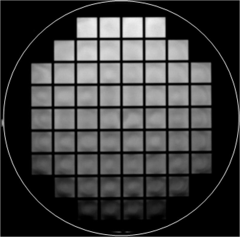
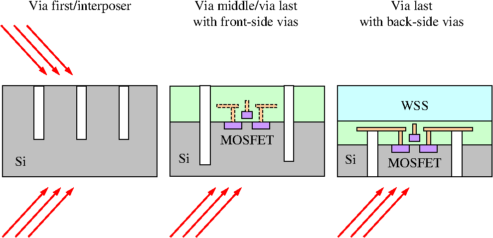
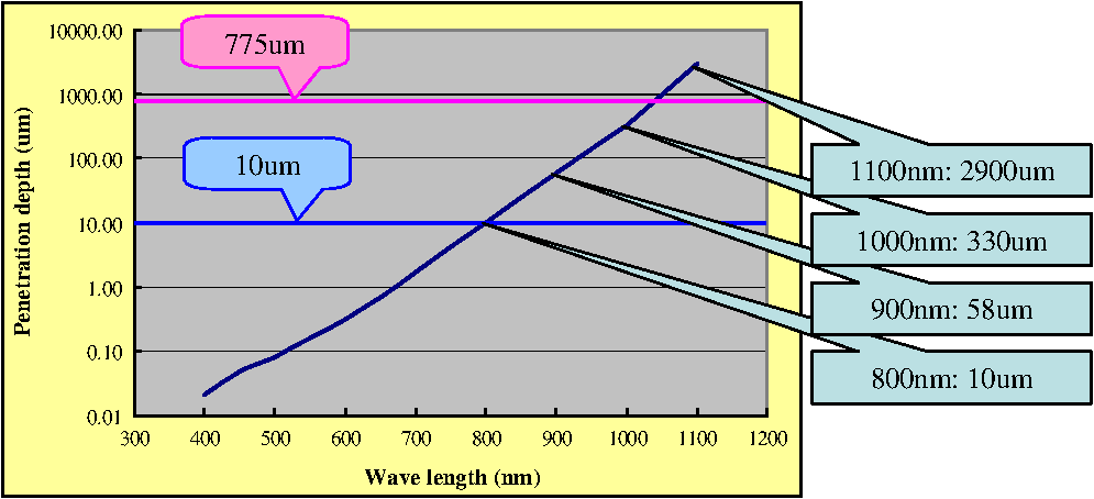
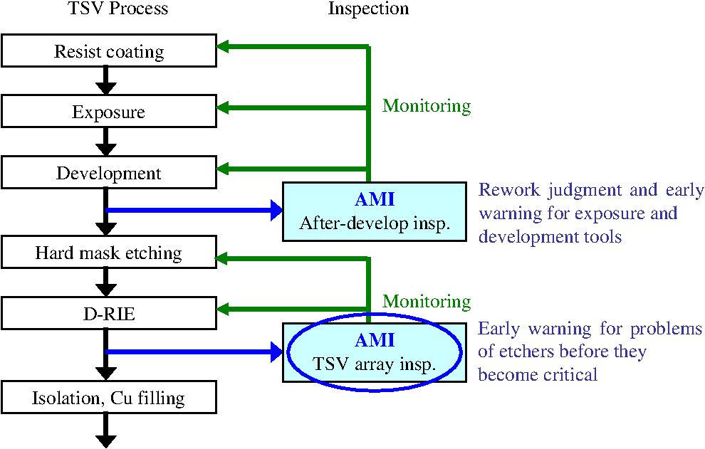
1.4.TSV Array Inspection Utilizing Diffraction Inspection TechnologyThe point mentioned above—the importance of examining patterns in every region over the wafer with high accuracy—is the same in the lithography process. A pattern inspection system (microinspection system) is becoming more expensive and slower with lithography design rule shrinkage. The combination of macroinspection and analysis tools is the most efficient and economical method when the macroinspection system is sensitive to pattern profile variations. Macroinspection monitors and screens every wafer, and the detected changes are analyzed by critical-dimension scanning electron microscopy (CD-SEM) or other analysis tools when necessary. The automatic macroinspection system, named the AMI series, which has diffraction inspection modes, has been proven to be both highly sensitive to pattern shape variations and high throughputs.8,9 The system resolution is low (approximately 300 μm), but its signal intensity is sensitive to pattern changes due to focus variation in scanners, improving yield by providing early screening of lithography performance in leading-edge device production lines. In this work, the authors have developed a new methodology to inspect a TSV array by utilizing diffraction inspection technology and have evaluated its performance.10 2.Methodology2.1.Optical SystemFigure 2 shows the optical configuration for diffraction inspection. The wafer is illuminated by telecentric light of single-band wavelength, and the diffracted light from repeated patterns is captured by the image sensor as a one-frame image. Fig. 2.Optical configuration for through silicon via (TSV) array inspection utilizing diffracted light. 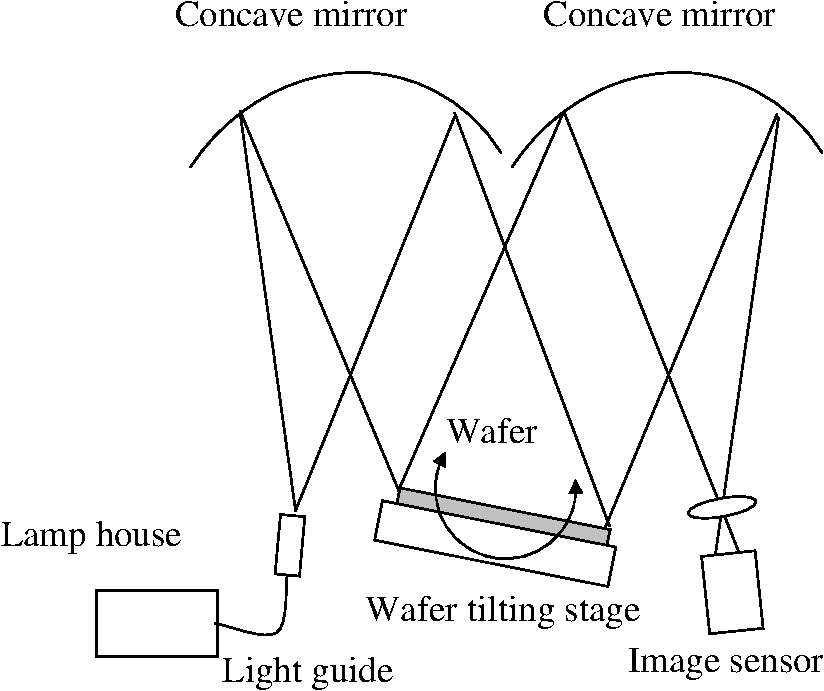 When repeated patterns are illuminated by light, diffracted light emerges to satisfy Eq. (1) as described below. The wafer tilting mechanism is installed in the system, and the wafer is tilted to satisfy the diffraction condition: where is the pattern pitch, the incident angle, the exit angle, the diffraction order, and the wavelength. Telecentric illumination is important to obtain diffracted light from the whole wafer in one shot. Every point over the wafer should be illuminated with the same incident angle, and diffracted light with the same exit angle should be captured. The optical parameters, such as wavelength, wafer tilting angle, and illumination power, are defined before the inspections so as to obtain sensitive signals for each wafer process.The diffracted light image of the whole wafer captured by the optical system is shown in Fig. 3. Obviously, the diffraction signal intensity in each area on the wafer changes as shown by the gray level, at which the variation depends on the hole size variation. The circle shows the wafer outline in Fig. 3 and the images obtained in this study. When the patterns are formed uniformly, the diffraction efficiency is uniform in every pattern area, and the image gray level is uniform. When cross-sectional pattern shapes in some areas are changed by defocusing of the exposure tool, for example, the diffraction efficiency in the area changes, and the image gray level becomes brighter or darker. The area resolution in the axis is not very high, but a slight change in cross-sectional pattern shape by error of the exposure or etching tool can be detected as the grayscale changes in the image. Diffraction occurs at the boundary of two materials with different refractive indices; therefore, the method is applicable to each stage of TSV formation such as after deep hole etching or after isolation/barrier-metal coverage. Here, this type of inspection is called “TSV array macroinspection.” 2.2.Inspection Opportunities in Various ProcessesFigure 4 shows the inspection opportunities in various TSV processes. In the case of the via first process or silicon interposer, holes (vias) are created on a bare silicon wafer. The hole pattern shape can be inspected from both front and back sides. In the case of the via middle or via last process with front-side vias, vias are created after metal oxide semiconductor field-effect transistor (MOSFET) fabrication. Inspection from the front side is difficult because of the presence of doped ions and wiring patterns, which block light. However, inspection from the back side is possible and effective in this case. In the case of the via last process with back-side vias, vias are created after MOSFET and interconnect fabrication, and after wafer support system attachment. Inspection from the front side is difficult, but that from the back side is possible. 2.3.Wavelength of Illumination LightRegarding illumination light, a single-band light is selected from the visible and near-infrared (NIR) light range. By using NIR light such as that of 1100-nm wavelength, it is possible to detect the change in hole shape in a deep position, including the bottom position because of Si transparency. The NIR light illumination capability was installed to detect the defects in deep positions of the wafer. 2.4.Defect Depth DiscriminationWhen the inspection is finished, a set of information including defect location information is sent to the host computer. In the case of TSV array inspection, it is better to consider depth (-axis) as well as -axis coordinates. Defect depth information can help defect source analysis and can also reduce the time of feedback to the exposure or etching tool. Silicon’s complex refractive index changes continuously according to the change in wavelength. Table 2 shows the list of and for typical wavelengths. The imaginary part of the index (), the absorption-related part, becomes smaller when the wavelength becomes larger than 400 nm, and it is almost zero at a wavelength of 1100 nm. This means that when the wavelength changes from 400 to 1100 nm, transmission increases; therefore, we can control the transmittance factor by choosing the wavelength. Table 2List of n and k for typical wavelengths.
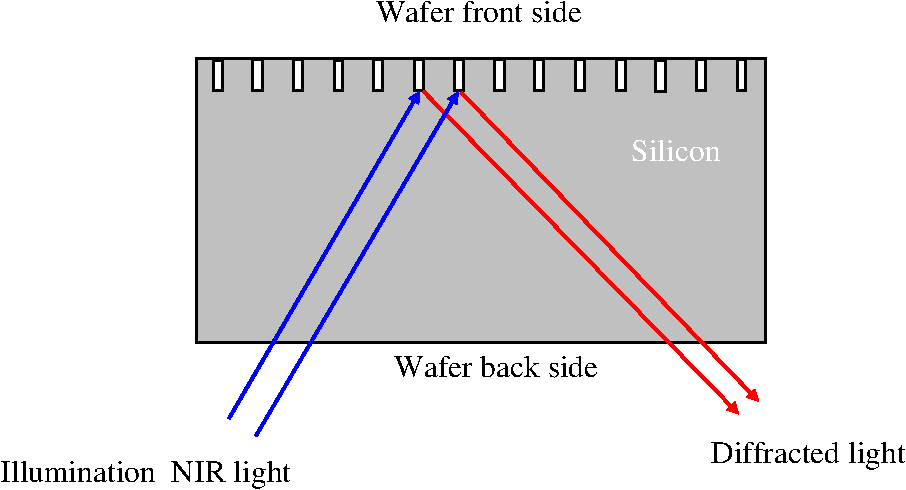
It is possible to discriminate the defect depth if we perform multiple inspections with different wavelengths, i.e., different transmittances. In other words, when the target defect type is specified, we can perform an optimized inspection by choosing the wavelength for the target defect depth. Figure 5 shows the penetration depths obtained for various wavelengths. Penetration depth means the depth where the light intensity decreases at the position. Penetration depth was calculated using Eq. (2): where is the penetration depth, is wavelength, and is the imaginary part of the index.2.5.Diffraction Inspection from Back SideThe shape of the bottom of the hole is important for controlling the process. As shown in Fig. 6, diffraction inspection from the back side of the wafer is suitable for checking the shape at the bottom, since the diffraction light intensity at the bottom becomes relatively larger than those of the other parts of the hole. However, the combination of diffraction inspections from the back and front sides is more effective for determining the defect location. 2.6.Profile Change Type DiscriminationThere are many profile changes, such as those of CD, depth, sidewall angle, and scalloping, and two or more profile changes can occur simultaneously in the production line. The effect of each profile change on signal intensity is nonlinear, and signal separation is complex. The signal separation for such cases is not included in this study; thus, we need to further study signal separation in each profile change. However, macroinspection with diffraction optics is still a powerful tool to manage production lines. Such diffraction inspection can indicate that a problem occurs in the production line, and information related to this problem, such as the location and shape of the defective area in the wafer and the specific wafer and lot, suggests the nature of the problem in the production line. This diffraction inspection can also indicate the point where further analysis should be carried out by measurement and analysis tools. The macroinspection with diffraction optics monitors every production wafer and provides early warning for problems in the production line. 3.Test ConditionsThe authors fabricated test wafers to evaluate the detection performance of the new methodology. The illumination light at a wavelength of 1100 nm was used. The light source used was a halogen lamp, and the narrow band of 1100-nm wavelength obtained using an interference filter was applied. Here, is 0.00003, and the penetration depth is approximately 3 mm, as shown in Fig. 5. The sensitivity of the image sensor chip is, however, very low at this wavelength; hence, the authors used a cooled camera to ensure an excellent SNR. The camera used was Hamamatsu ORCA-AG. In addition, other wavelengths, such as 850, 800, 700, 546 (e-line), 436 (g-line), and 405 (h-line) nm, were also investigated. Table 3 shows the list of test wafers. Bare 200-mm silicon wafers were etched by deep reactive-ion etching (D-RIE), and the hole of 5-μm diameter and 50-μm depth was arrayed with a 10-μm pitch. Diffraction images with various conditions were captured, and diffraction signal intensity was analyzed. Wafer A was considered to have a standard pattern, and the signals of the other wafers were compared with that of wafer A, assuming that the pattern shape changes from that of wafer A to those of the other wafers. Table 3List of test wafers.
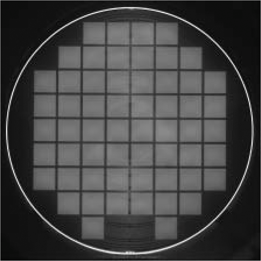
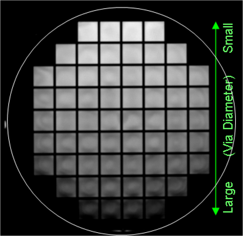
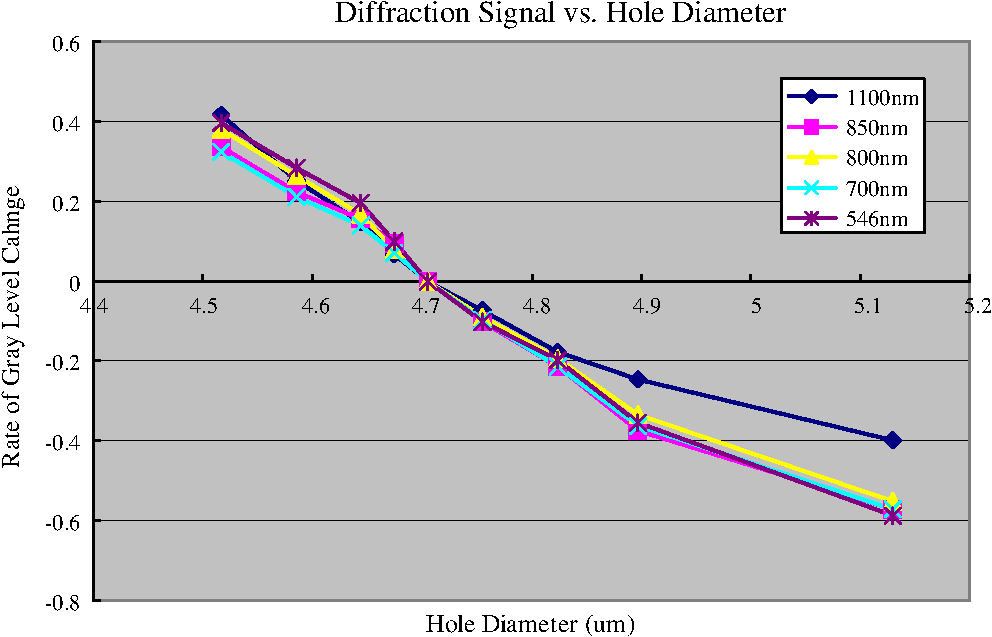
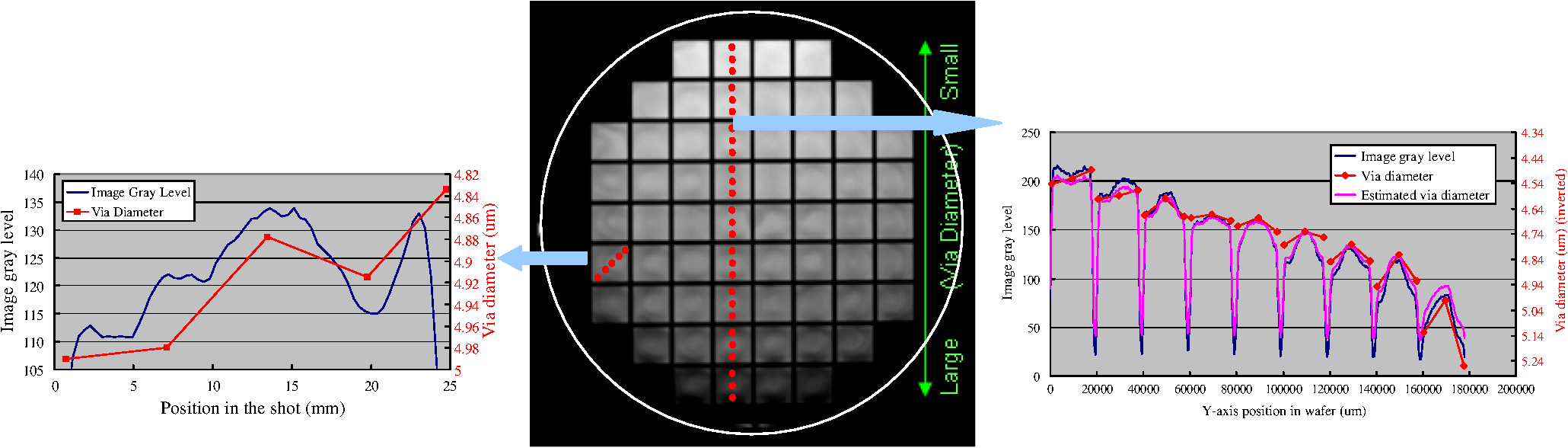
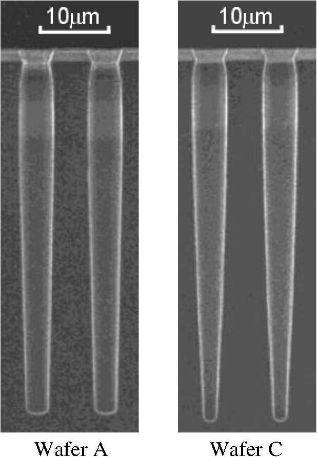
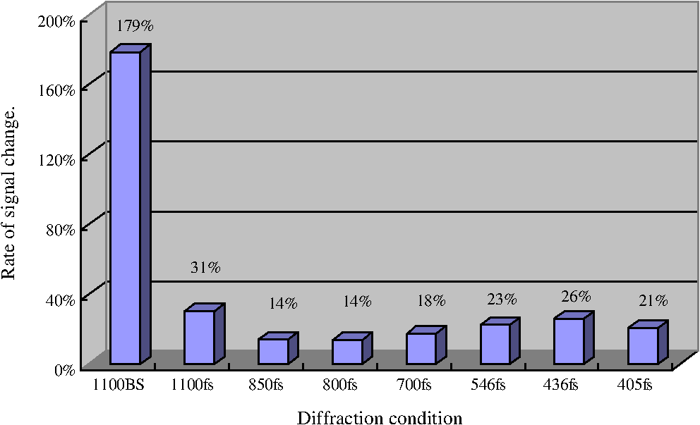
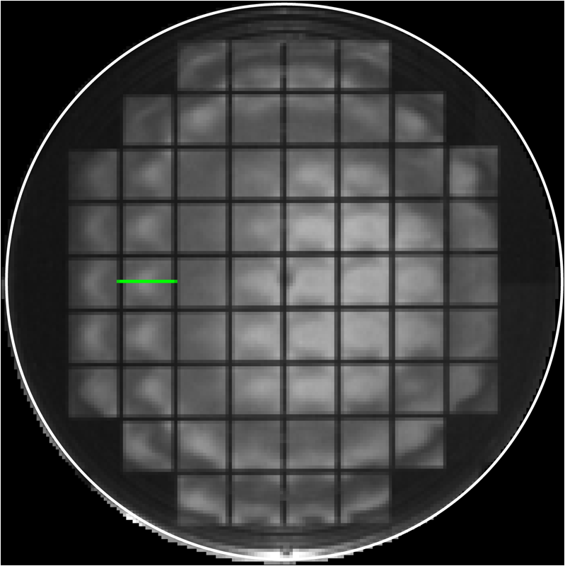
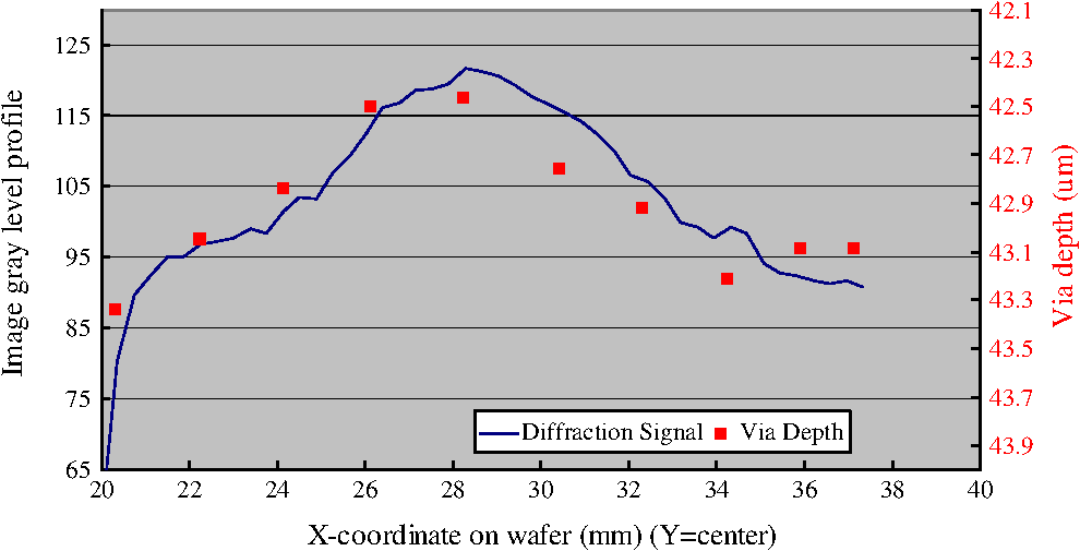
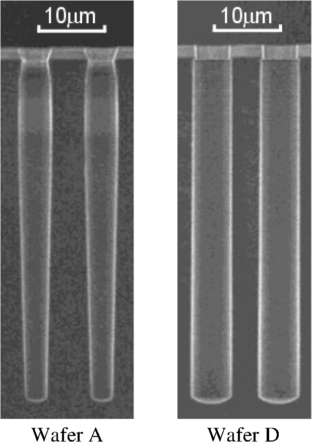
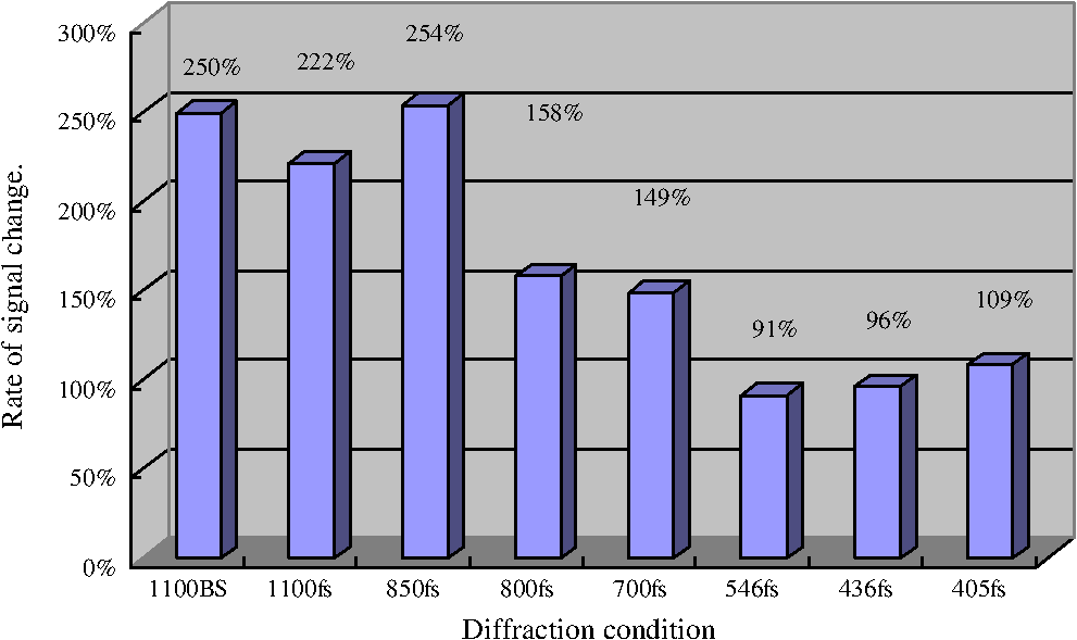
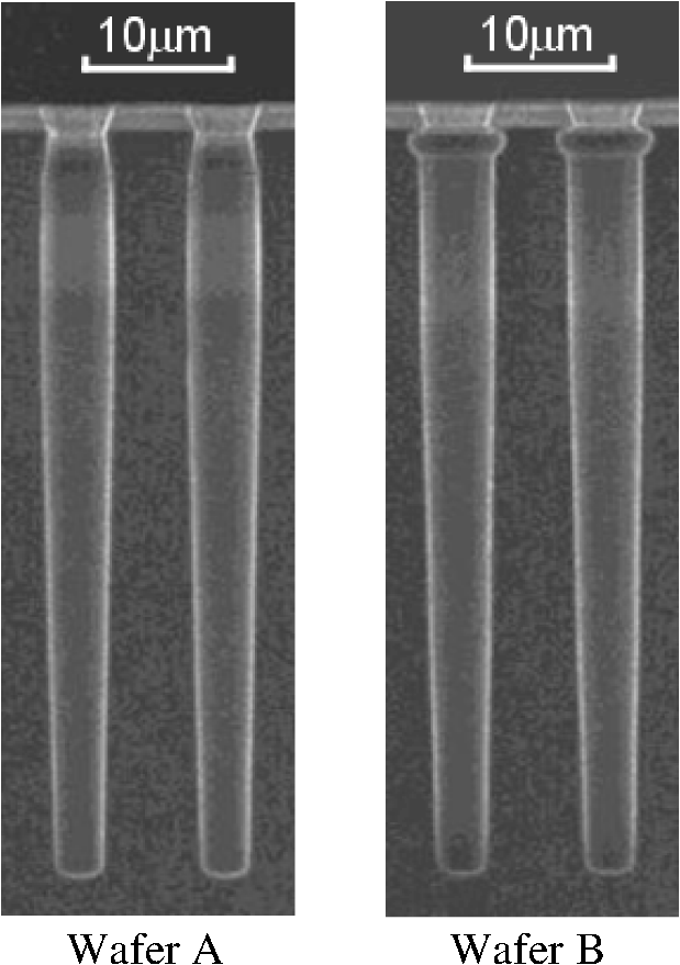
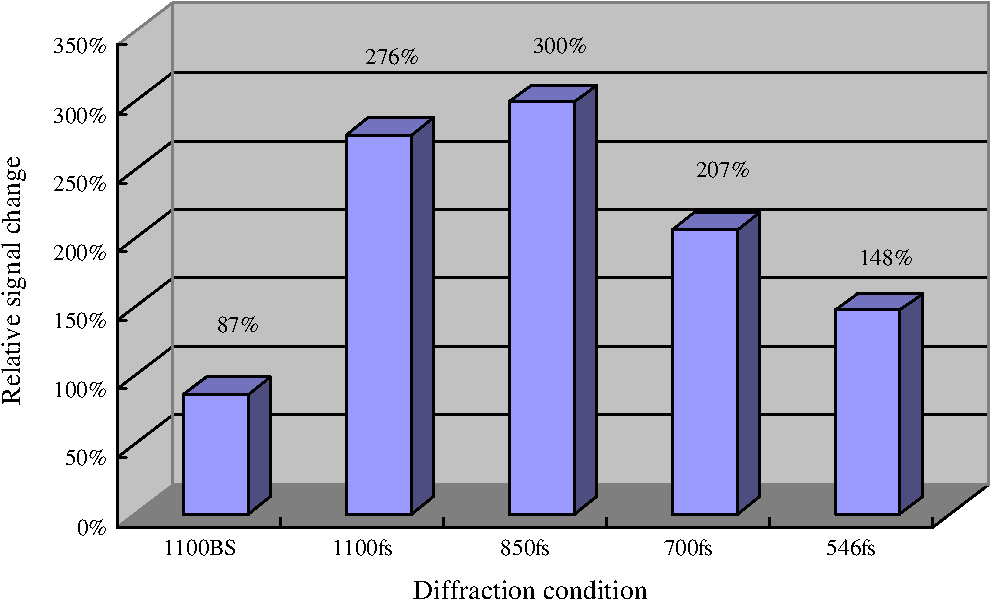
4.Test ResultsThe diffraction image of each test wafer was captured. Figure 7 shows the sample diffraction image, with wafer A, at the fourth-order diffraction light wavelength of 1100 nm. An almost-uniform diffracted light was captured from each shot of the wafer. 4.1.Detection Sensitivity to Hole Diameter VariationWafer E has various hole diameters produced by exposure to dose offsets on the exposure tool. Each row has a different dose setting; thus, each row has a different diameter after etching. Figure 8 shows the diffraction image of wafer E. The relationship between diffraction signal intensity and hole diameter is shown in Fig. 9. The -axis indicates hole diameter, and the -axis the rate of gray-level change relative to that at the diameter of 4.7 μm in Fig. 9. The rate of gray-level change is defined by Eq. (3): where is the averaged gray level of the center shot (column 4) of each row and is the averaged gray level of the center row (row 5). was approximately 150. Regarding the hole diameter, the top diameter was measured by CD-SEM, and the hole diameter of the center row was 4.71 μm.As shown in Fig. 9, the diffraction signal changes almost linearly according to hole diameter changes. From Fig. 9, it was calculated that the signal change for a 10-nm-diameter change was 2.5 image gray levels (1.67% of ); this is large enough to be detected. Furthermore, in Fig. 8, within the one-shot area, the pattern profile obviously varies owing to the exposure tool’s shot variation. In addition, at the edge of Si wafers, a slight intensity modulation was detected, and such modulation was caused by D-RIE’s plasma density dependence. Figure 10 shows the relationship between diffraction signal intensity and hole diameter indicated by the dotted red lines on the diffraction wafer. A high correlation between diffraction signal intensity and hole diameter was observed. The magenta line in the righthand graph in Fig. 10 shows the diameter calculated from the diffraction signal intensity. The linear approximation of the 546-nm graph in Fig. 9 was used to convert the diffraction signal intensity to the diameter. The magenta line shows good estimation. In summary, this inspection method is considered suitable for tool condition monitoring of the exposure system and D-RIE. 4.2.Detection Sensitivity to Shrinking BottomWafers A and C have almost the same diameter at the opening of the holes; however, wafer C has a smaller diameter relative to the depth than wafer A. SEM images are shown in Fig. 11. Diffraction images were captured from both front and back sides, at various wavelengths and diffraction orders, and then the images were analyzed. The maximum signal changes according to the pattern changes from wafer A to wafer C at various diffraction orders were extracted and are compared in Fig. 12. 1100BS is the signal of the back-side diffraction at 1100 nm, and 1100 fs is the signal of the front-side diffraction. The signal of wafer A is defined as 100%. 1100BS shows a significant change at 179%. This means that the diffraction light intensity at the bottom is relatively larger than those in the other parts of the hole in the diffraction inspection from the back side. The largest signal change in the front side group at 1100 nm is 31%. It is concluded that diffraction inspection from the back side is effective for detecting the defect around the hole bottom. 4.3.Detection Sensitivity to Hole Depth VariationsFigure 13 shows the diffraction image of another wafer (wafer ), which was formed under similar conditions to wafer A. Note that the etching condition of this wafer was not well optimized compared with that of wafer A. A characteristic doughnut signature is observed. We broke the wafer, then measured the hole depth profile along the green line in Fig. 13, and compared it with the image grayscale profile. We can see a correlation between the gray level and hole depth profiles, as shown in Fig. 14. However, the diffraction signal may change according to not only the hole depth variation but also other types of shape change. Hence, the grayscale variation in Fig. 13 suggests the combination of various types of pattern profile change generated by D-RIE. By further analysis of these results, it is expected that the technology will be enhanced to a higher level of shape profile measurement. 4.4.Detection Sensitivity to Sidewall RoughnessThe authors evaluated the detection sensitivity to sidewall roughness. The Bosch process is known as the method of forming hole patterns with a high aspect ratio. However, this process may form a typical roughness on the sidewall, and it may cause a problem in obtaining TSVs when the roughness is large. A large roughness was intentionally produced on the sidewall of hole patterns on wafer D. Cross-sectional SEM images are shown in Fig. 15, and signal changes are shown in Fig. 16. Large signal changes are observed at long wavelengths. However, the shape changes between wafer A and wafer D are related to not only sidewall roughness but also hole diameter. Hence, the signal changes include the responses of both roughness and diameter differences. 4.5.Detection Sensitivity to UndercutThe holes of wafer B have a large opening generated by undercut. Cross-sectional SEM images are shown in Fig. 17, and signal changes are shown in Fig. 18. Large signal changes are observed from the front side, even with short wavelengths. This makes sense, because the large opening is the defect on the surface of the wafer. The sensitivity from the back side is relatively small, since the signal from the opening is relatively small. However, even from the back side, the sensitivity is high enough to be detected. 5.Proposed OperationFigure 19 shows the proposed operation in the TSV process. TSV array macroinspection after D-RIE can monitor both hard mask etching and D-RIE during the creation of TSVs. In addition, it is recommended to execute a litho-oriented macroinspection as after-development inspection to eliminate coating, exposure, and developmental issues. 6.ConclusionsAs a new method of determining the profile uniformity of a TSV array, the performance of diffraction inspection with NIR light was evaluated. First, it was confirmed that diffraction inspection could detect the hole pattern array defect around their opening (wafer surface) with visible light, i.e., without NIR light. The sensitivity was high enough to detect a 10-nm diameter change under test conditions. Then, it was confirmed that by using NIR light and backside diffraction, feature variations at large depths could be effectively detected. The quantitative correlations between diffraction signal and pattern shape changes were found. The new method could detect the pattern variation profile over the wafer by D-RIE. By choosing or combining the different conditions, such as different wavelengths on the front and back sides, a more effective inspection and defect depth discrimination was made possible. The performance test was done using test wafers with arrayed holes on bare silicon; however, the method is also applicable to other stages of TSV creation. In this study, the authors fabricated test wafers with dense TSV (hole) arrays and carried out experiments on them. Memory device wafers may have TSV arrays with a steadily repeated pitch; therefore, the method is applicable to process wafers of memory devices. In the case of logic devices, it is possible to manage exposure and etching tools with test patterns as quality control. In conclusion, this new TSV inspection methodology should be viable for various types of high-volume manufacturing device fabrication. ReferencesInternational Technology Roadmap for Semiconductors, 2010 Update,
(2013) http://www.itrs.net/Links/2010ITRS/2010Update/ToPost/2010Tables_Interconnect_FOCUS_E1_ITRS.xls Feb. ). 2013). Google Scholar
“3-D IC integration & TSV interconnects, 2010 Market Analysis,”
133
(2010). Google Scholar
K. Okamoto,
“Importance of wafer bonding for the future hyper-miniaturized CMOS devices,”
ECS Trans., 16
(8), 15
–29
(2008). http://dx.doi.org/10.1149/1.2982850 1938-5862 Google Scholar
“Via First vs. Via Last? The first study to understand 3-D integration scenarios,”
(2010). Google Scholar
P. Morrowet al.,
“Three dimensional wafer stacking via Cu-Cu bonding integrated with 65-nm strained-Si/low-k CMOS technology,”
IEEE Electron Dev. Lett., 27
(5), 335
–337
(2006). http://dx.doi.org/10.1109/LED.2006.873424 EDLEDZ 0741-3106 Google Scholar
D. Marxet al.,
“Non-destructive TSV etch depth uniformity measurement,”
in SEMATECH Workshop on 3-D Interconnect Metrology,
(20102013). http://www.sematech.org/meetings/archives/3d/8971/posters/Marx.pdf Google Scholar
E. NovakJ. Schmit,
“Through silicon via (TSV) metrology with white light interference microscopy,”
in SEMATECH Workshop on 3-D Interconnect Metrology,
(20102013). http://www.sematech.org/meetings/archives/3d/8971/pres/Veeco%20TSV%20Metrology%20Semicon%20West%202010.pdf Google Scholar
K. Komatsuet al.,
“Automatic macro inspection system,”
Proc. SPIE, 3677 764
–771
(1999). http://dx.doi.org/10.1117/12.350863 PSISDG 0277-786X Google Scholar
T. Kitamuraet al.,
“Automatic macro inspection system,”
Proc. SPIE, 3998 615
–621
(2000). http://dx.doi.org/10.1117/12.386514 PSISDG 0277-786X Google Scholar
Y. Fujimoriet al.,
“A new methodology for TSV array inspection,”
Proc. SPIE, 7971 79710I
(2011). http://dx.doi.org/10.1117/12.879379 PSISDG 0277-786X Google Scholar
Biography |