|
|
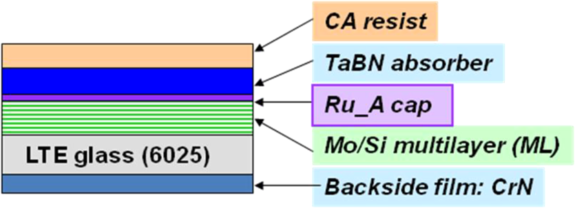
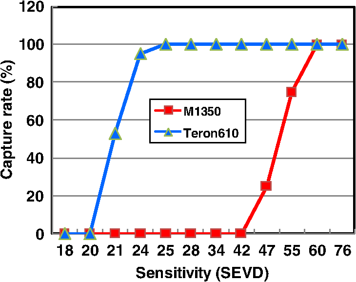
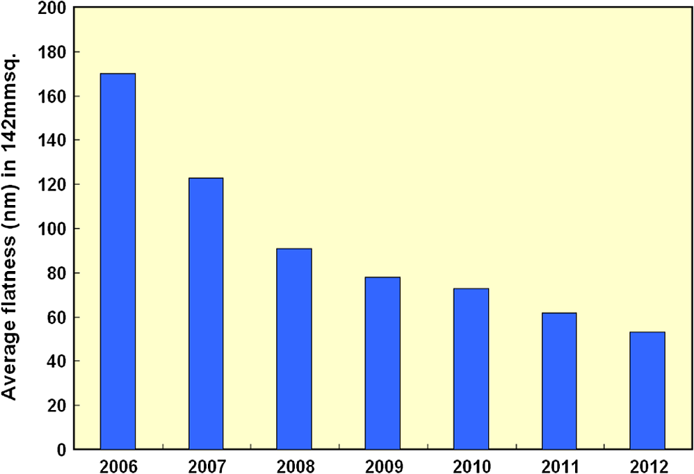
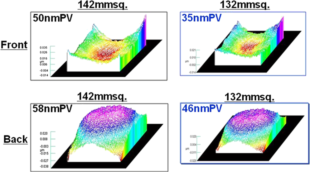
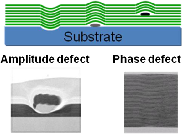
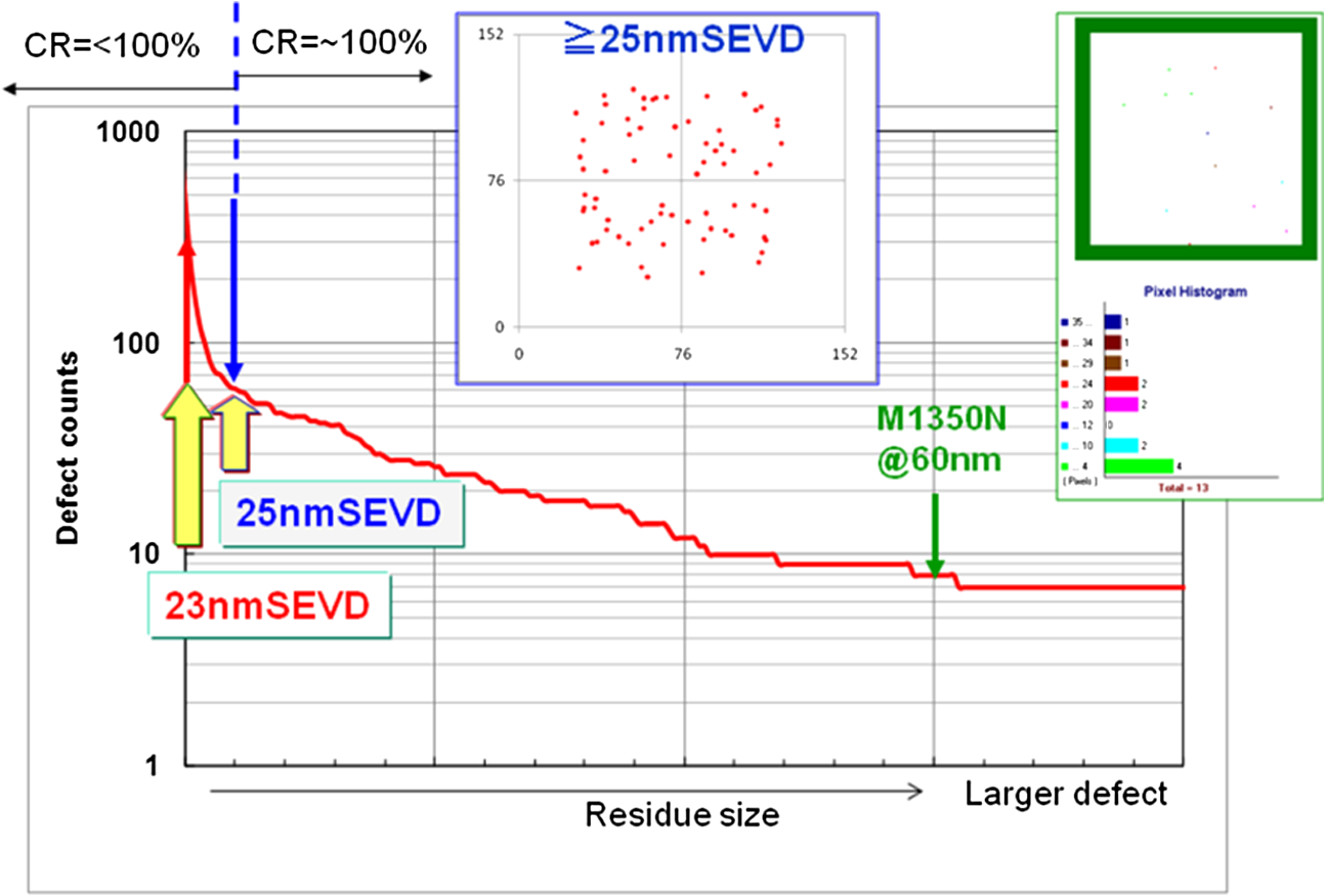
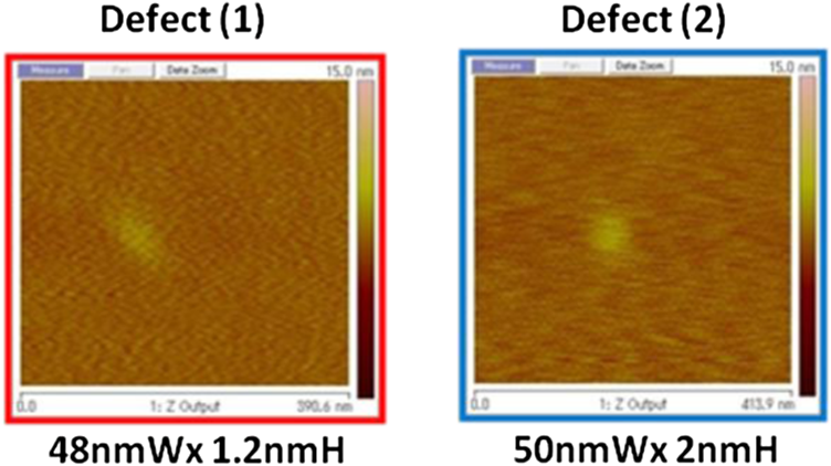
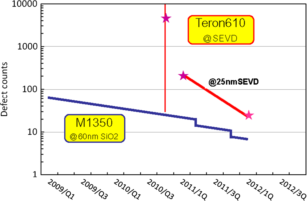
1.IntroductionExtreme ultraviolet (EUV) lithography is a leading candidate for manufacturing semiconductor device at 22 nm half-pitch (hp) and beyond, and several devices have been developing and evaluating using EUV lithography toward volume production. Defect-free EUV mask with high flatness substrate is one of critical challenges in implementing EUV lithography. Figure 1 shows structure of typical EUV mask blank. An EUV mask is composed of a reflective multilayer (ML) consisting of molybdenum (Mo) and silicon (Si), and a patterned absorber layer formed on a glass substrate with low thermal expansion (LTE). A LTE glass material with a maximum coefficient of thermal expansion of 5 ppb is required to minimize thermal distortion in an EUV exposure process. ULE™ of Corning has been applying as LTE glass material. An EUV blank consisting of a ML, a ruthenium (Ru) capping layer and a tantalum boron nitride (TaBN) absorber has been developing.1,2 The Ru is an excellent protecting layer against dry etching and repair processes of the absorber in mask making process. The EUV blank must have a conductive film on the back side for electrostatics chucking on the reticle stage in an EUV exposure tool. A chromium nitride (CrN) film has been popularly using as back side film. Excellent pattern performance of the TaBN absorber has been verified.3,4 There are two critical issues related to the EUV blanks. The first issue is high flatness for the glass substrates. In the case of optical mask blanks, flatness on the mask is mainly affected by depth of focus only in optical lithography process. On the other hand, non flat surface on the EUV mask affects undesirable image placement error (IPE) on the wafer caused by nontelecentric illumination with incident angle of 6-deg in EUV exposure. Relationship between IPE and flatness error () can be expressed by , where is reduction ratio of optics and is incident angle. Flatness error of 50 nm peak-to-valley () on the mask surface causes IPE of 1.3 nm on the wafer in EUV lithography with optics (). It means that a flatness error on the mask surface causes degradation in overlay performance in device manufacturing. Requirement of substrate flatness should be decided to meet a certain budget of overlay required in EUV exposure process. As the surface on the mask stage is a reference flat, back side on the mask must have high flatness as well as the flatness on the front side. The second issue is defects on the ML blanks. Defect size required for the ML blanks should be same as that of the optical mask blanks in the same technology node. However, defects with a few nanometer in height cause unacceptable critical dimension (CD) variation on the wafer in EUV exposure process as phase defects. This defect height is more than 20 times tighter than that for optical masks for 193 nm lithography with argon fluoride (ArF) laser due to main difference in wavelength. Moreover, as it is very difficult to repair the defects on the ML blanks, zero defects have to be achieved on raw ML blanks. According to simulation results,5 a defect with 60 nm in full width half maximum (FWHM) and 1.3 nm in height, corresponding to 22 nm sphere-equivalent-volume-diameter (SEVD), would cause CD variation of as printable defects at the 22 nm hp. Defect inspection tool with higher sensitivity is very important to manage and to improve small defects like a 22 nm SEVD. Traditionally, sensitivity of defect inspection is defined using sphere particle like poly-styrene latex (PSL) and as standard. However, in case of phase defects with low height on an EUV blank, it is impossible to discuss from sensitivity of particle. Recently, definition of SEVD was newly made as common standard for actual phase defects. A Lasertec M1350 and M7360 have sensitivity of 60 and 45 nm , respectively, which are insufficient for the target of 22 nm SEVD.6 Two kinds of inspection tools have been reported as next generation tools at the 22 nm hp and beyond. One of them is Teron blank inspection with 193 nm light developed by KLA-Tencor, known as Phasur, which is commercially available.7 The other one is actinic inspection tool with an EUV light that MIRAI-Selete have developed.8 It is facing to develop prototype tool in a program at EUVL Infrastructure Development Center, Inc. (EIDEC). Improvement of EUV blanks have been reported under inspection of M1350.2 In this paper, further improvements of flatness and defects on EUV blanks will be described. 2.EUV Blanks Fabrication ProcessLocal polishing has been carried out as main process to make a glass substrate with high flatness after conventional global polishing. Local polishing technique with numerical control (NC) using flatness data, known as figure correction of mirrors, is appropriate for achieving precise flatness control for the EUV mask substrates. Then, touch polishing is done to remove some surface damage caused by the local polishing process. After that, cleaning process is carried out for the polished substrates to effectively remove polishing slurry and particles. A flatness of a substrate is measured by a UltraFlat of Corning-Tropel. A Mo/Si ML film, consisting of 40 bi-layers of Si and Mo, and a Si capping layer was deposited on the polished glass substrate using the ion beam deposition (IBD) method. The Si capping layer with a thickness of 4 nm was formed to prevent oxidation of the underlying Mo layer. Periodic length of Mo and Si layers and thickness of Si capping layer were measured on the ML blanks using X-ray reflection (XRR) method. The ML blanks are annealed in air to reduce a stress of the ML film. The EUV reflectivity performance such as centroid wavelength can be precisely estimated from the measured periodic length using an optical simulator. Then, a Ru capping layer and an LR-TaBN absorber are deposited on the ML blank using dc magnetron type sputtering tool. A CrN film is coated on the back side of the blanks for electrostatic chuck on a mask stage in an EUV exposure tool. An electron beam (EB) resist is coated on the blank; then the blank is baked in a hot-plate baking system. Defect inspection is performed on the substrates, ML blanks, and EUV blanks using a M1350. The M1350 has equivalent sensitivity of 60 nm on the ML film in production. Late 2010, inspection of a Teron610 Phasur was started for development work. The Teron610 is very valuable for further reduction in smaller defects on a ML blank. Inspection capability was checked using a programmed defect ML blank (PDM).9 The PDM has defect cells with different sizes as bump type defects. Size of each defect cell was defined as SEVD value using atomic force microscopy (AFM) measurement. Capture rate (CR) of each defect cell was measured as inspection capability in the M1350 and the Teron610, as shown in Fig. 2. The M1350 has sensitivity of 60 nm SEVD. The Teron was confirmed to have sensitivity of 25 nm SEVD with a CR of 100%, and sensitivity of 21 nm SEVD with around 50% CR. The Teron Phasur would be covered for 22 nm hp process at least, and it is expected that the sensitivity will be improved for 16 nm hp. 3.Substrate Flatness ImprovementAccording to the ITRS2011,10 glass substrates with a flatness of 26 nm and 18 nm on the both sides are required for an EUV mask in the 23 nm hp and 16 nm hp process, respectively. These are quite tight for blank manufacturing, and ideal requirements in an EUV exposure process without any correction to meet certain overlay budget for each hp node. Recently, flatness correction technique using flatness data on the blanks is being developed11 to correct an image placement caused by the flatness error in mask making process. It has been expected that the flatness requirement would be relaxed using flatness correction process. We were doing continuous improvement of polishing process to meet the ideal requirement since 2006. Figure 3 shows actual trend of improvement of flatness quality from 2006 to 2012.2 An average flatness of on substrates made under the improved condition in each year was plotted in the figure. A is a quality area for flatness control, which corresponds to an area of electrostatics chucking. Key is optimization of local polishing process and high accurate flatness measurement to improve the flatness. In 2008, a substrate with around 90 nm was achieved as average performance by applying local polishing process, and fundamental polishing process was established for a flatness of less than 100 nm as first step. After that, improvement of productivity in local polishing process as well as flatness improvement has also been done. Then, the flatness was improved to around 50 nm in 2012 through development of more precise polishing process including more accurate flatness measurement. As shown in the trend, flatness quality has been steadily improving through continuous improvement of polishing process, and a substrate with a flatness of 30 nm on both sides was achieved as best. However, current process including accuracy of a flatness measurement tool might be restricted to attain a flatness of less than 30 nm with excellent reproducibility in volume production. Originally, quality area of flatness was , corresponding to electrostatics chuck area in an EUV exposure tool. Smaller quality area like a maximum exposure area should be applied for practical usage in an EUV exposure process. Figure 4 shows flatness maps in 142 mm and in area on both sides on typical substrate produced by the improved process. Small area of is effective to make higher flatness as expected. Practical specification should be made in smaller quality area of using flatness correction process in addition to further improvement in the flatness. 4.ML Blank Defect QualityThere are two types of defects on a ML blank as shown in Fig. 5. One of them is large defect, called amplitude defect, mainly caused by ML coating process. This would be critically printable due to large loss of reflectivity at EUV light. It is impossible to completely judge amplitude defects from defect inspection data because current inspection process cannot see height of defects. Major parts of large defects over around 150 nm would be amplitude defects based on our analysis data. The other one is small defect, called phase defect, which has low height of around 10 nm and less. It has been confirmed that almost small defects captured as 150 nm and less originate on a substrate caused in polishing and cleaning processes. Large defects should be zero because of its difficulty of repair. And we are reducing large defects though improvement of ML coating process. Printable small defects also should be improved mainly through optimization of substrate process. Some of them can be mitigated and/or repaired by a defect compensate process.12,13 It was expected that phase defects of around 10 over 22 nm SEVD can be accepted for 22 nm hp process using some defect compensate processes. Defect reduction on the ML blanks has been performing in the M1350 inspection with 60 nm sensitivity since 2004. Since late 2010, a Teron blank inspection with sensitivity of 22 nm SEVD has been using for further defect reduction of smaller defects. There are two kinds of defects caused by substrate finishing process. One of them is a pit type defect caused by mechanical damage in polishing process. The other one is a bump type defect. It would be remaining polishing slurry and additional foreign material in substrate finishing process. Defects over 60 nm on the ML blanks have been steadily reduced by improving substrate finishing and ML coating processes. Low defects of single digit over 60 nm have been produced. Total three defects inspected by M1350 were achieved as the best as shown in Fig. 6. Figure 7 shows inspection data on a ML blank in area inspected by the Teron. It indicates relationship between total defect counts and residue size. The residue means intensity of defect extracted by the Teron, corresponding to defect size. Sensitivity points of 23 nm SEVD and 25 nm SEVD were put in this inspection data under standard inspection condition. The blank has 13 defects in area as shown in the map. Defects monotonically increase down to 25 nm SEVD as defect size decreases. Small defects below 25 nm SEVD exponentially increase. Actual size of small defects captured by the Teron only was measured by AFM. Figure 8 shows AFM images of typical two defects inspected by Teron610. It has confirmed that there are small defects with low height of less than 2 nm on the ML blank that the Teron can capture. In order to reduce small defects on a ML blank, fabrication process of substrates has been mainly improving. Most of efforts are meant to effectively remove particles (slurry and foreign material etc.) caused in polishing by modification of cleaning process and to improve pit defects by improvement of polishing process. Actual trend of defects on a ML blank is shown in Fig. 9. As above described, 70 defects over 60 nm in 2009 were steadily reduced to single digit. And more than a few thousand defects were observed in initial Teron inspection. The inspection including some false defects was done under nonoptimized inspection condition. After that, inspection condition was optimized without false defects. Various improvements in substrate finishing and ML coating processes were tried to reduce small defects. A few hundred defects over 25 nm SEVD were existed on the blank made in the first quarter of 2011. The defects were dramatically improved to 20 defects in the Teron inspection as one of the best results. That means several approaches for improvements in fabrication process were effective to reduce small defects. Surely, a gap in defects between actual quality and the target is getting small by continuous improvement. And we are facing to reduction in smaller defects over 23 nm SEVD as next phase toward production with 22 nm hp process. 5.ConclusionTwo critical issues of flatness and defects must be improved on an EUV blank for near future volume production. Flatness of a substrate has been steadily improving by more modification of polishing process including local polishing. Around 50 nm as average and 30 nm as best were achieved in area. However, it is not easy to make a flatness of less than 30 nm in current process. A quality area of is too wide compared with actual exposure area of . As smaller area is effective to produce better flatness, practical quality area like a maximum exposure area of should be decided for blank manufacturing. And practical flatness also would be specified through progress in actual flatness correction process and further flatness improvement. Defect quality on a ML blank has been reduced to single digit over 60 nm inspected by a M1350 by improvement of fabrication process. Defect reduction on a ML blank was moved to new defect inspection of a Teron610 Phasur. The Teron has high sensitivity of 22 nm SEVD meeting requirement for 22 nm hp process. It was confirmed that it can capture real phase defects with 50 nm in width and low height of 2 nm under a condition of 25 nm SEVD. There are a thousand of small phase defects on a ML blank in initial Teron inspection. The defect was dramatically reduced to 20 defects mainly through various improvements of fabrication process. Great progress was made for defects and flatness on the EUV blanks in the past two years. Practical specifications of flatness and defects should be discussed through actual exposure test and usage of a correction process. AcknowledgmentsThe authors would like to thank Hisao Shirasugi of Blanks Division of HOYA Corporation for promoting this work. We also would like to thank Takamitsu Mochizuki, Kazumi Shimazu, Akihiko Ibe and other members of our EUV team who contributed to this work. ReferencesT. Shokiet al.,
“Process development of 6-inch EUV mask with TaBN absorber,”
Proc. SPIE, 4754 857
–864
(2002). http://dx.doi.org/10.1117/12.477007 PSISDG 0277-786X Google Scholar
T. Shokiet al.,
“Improvement of total quality on EUV mask blanks toward volume production,”
Proc. SPIE, 7636 76360U
(2010). http://dx.doi.org/10.1117/12.849363 PSISDG 0277-786X Google Scholar
T. Abeet al.,
“Process development for EUV mask production,”
Proc. SPIE, 6349 63493G
(2006). http://dx.doi.org/10.1117/12.692519 PSISDG 0277-786X Google Scholar
T. Abeet al.,
“EUV-mask pattern inspection using current DUV reticle inspection tool,”
Proc. SPIE, 6607 66070L
(2007). http://dx.doi.org/10.1117/12.728935 PSISDG 0277-786X Google Scholar
T. Terasawaet al.,
“Phase defect printability and actinic dark-field mask blank inspection capability analyses,”
Proc. SPIE, 7969 79690V
(2011). http://dx.doi.org/10.1117/12.879398 PSISDG 0277-786X Google Scholar
W. Choet al.,
“Inspection with the Lasertec M7360 at the SEMATECH mask blanks development center,”
Proc. SPIE, 6517 65170D
(2007). http://dx.doi.org/10.1117/12.712990 PSISDG 0277-786X Google Scholar
S. Stokowskiet al.,
“Inspecting EUV mask blanks with a 193 nm system,”
Proc. SPIE, 7636 76360Z
(2010). http://dx.doi.org/10.1117/12.850825 PSISDG 0277-786X Google Scholar
T. Terasawaet al.,
“High-speed actinic EUV mask blank inspection with dark-field imaging,”
Proc. SPIE, 5446 804
–811
(2004). http://dx.doi.org/10.1117/12.557814 PSISDG 0277-786X Google Scholar
T. Kinoshitaet al.,
“Fabrication of programmed phase defects on EUV multilayer blanks,”
Proc. SPIE, 5256 595
–606
(2003). http://dx.doi.org/10.1117/12.517836 PSISDG 0277-786X Google Scholar
, (ITRS2012); Lithography, Litho_2012 Tables_Table LITH 6, EUVL Mask Requirements,
() http://www.itrs.net/Links/2012ITRS/Home2012.htm Google Scholar
S. Raghunathanet al.,
“Correlation of overlay performance and reticle substrate non-flatness effects in EUV lithography,”
Proc. SPIE, 7488 748816
(2009). http://dx.doi.org/10.1117/12.834746 PSISDG 0277-786X Google Scholar
J. BurnsM. Abbas,
“EUV mask defect mitigation through pattern placement,”
Proc. SPIE, 7823 782340
(2010). http://dx.doi.org/10.1117/12.865160 PSISDG 0277-786X Google Scholar
R. Jonckheereet al.,
“Repair of natural EUV reticle defects,”
Proc. SPIE, 8166 81661G
(2011). http://dx.doi.org/10.1117/12.898864 PSISDG 0277-786X Google Scholar
Biography Tsutomu Shoki joined HOYA Corporation in 1986. He developed a panel for inorganic electroluminescence display and then an x-ray mask for proximity x-ray lithography until 1999. He joined EUV program at R&D center in 2000, and developed material and mask process for an EUV mask. Then he was transferred to the Blanks Division in 2007. He received a PhD from university of Hyogo in 2007. Currently, he is a manager of EUV blanks development.  Masato Ootsuka joined HOYA Corporation in 1982. He was an engineer related to polishing process for optical blanks until 2007. Then he worked for LCD blanks from 2007. He joined the EUV blank project in 2009. Currently, he is a team leader of polishing process in EUV blank production.  Minoru Sakamoto joined HOYA Corporation in 1984. He was a production engineer for optical blanks in Blank division. He was transferred to MD division in 1987, and worked as production engineer until 2002. He was transferred to Blank division in 2002, and he was in charge of improvement of optical blank production. He joined the EUV blanks project in 2009. Currently, he is in charge of production and improvement of EUV blanks.  Tatsuo Asakawa joined HOYA Corporation in 1998. He was a production engineer for optical blanks until 2005. Then he worked in production of LCD blanks until 2008. He worked as deposition process engineer for advanced optical blanks in 2009. He joined the EUV blanks project in 2009. Currently he is in charge of production and improvement of EUV blanks.  Ryuuji Sakamoto joined HOYA Corporation in 1979. He worked as a production engineer for optical blanks. Then he joined the EUV blank development department in 2010. Currently, he is a leader of EUV blank production.  Hirofumi Kozakai joined HOYA Corporation in 2005 and was a production engineer related to cleaning process for optical blanks. He was in charge of cleaning process in LCD blanks production from 2006. He joined the EUV development department in 2011. Currently, he is an engineer related to deposition process for EUV blanks.  Kazuhiro Hamamoto joined HOYA Corporation in 2006 and he has been engaged in EUVL and nano-imprint mask R&D. Currently, he is an engineer related to inspection for EUV blanks. He received BS degree and PhD degree in material engineering from Himeji Institute of Technology in 2001 and 2006, respectively.  Takahiro Onoue joined HOYA Corporation in 2005. He was in MD (memory disk) division that dealing with magnetic recording media for HDD, and in charge of development to improve areal recording density of PMR (perpendicular magnetic recording media) until 2010. He was transferred to corporate development office in 2011. Currently, he is a development engineer in EUV blanks development team. He received PhD degree from Waseda University in 2000. He established academic background in 2000 to 2005, as a lecturer in Waseda University, and as a post doc researcher in the University of Twente, in the Netherlands.  Toshihiko Orihara joined HOYA Corporation in 2011 and joined the EUV blanks project. Currently, he is an engineer of EUV blanks development.  Osamu Maruyama joined HOYA Corporation in 1986. He developed optical components and non-linear optical device for optical communication by 1999 and researched and developed the new polishing method for HDD glass disk and mask blanks. He worked by an LCD blanks production factory setup and managed production in Malaysia from 2005 until 2011. He engaged in the setup of the EUV new line on 2011 in Japan. Currently, he is a manager of EUV production engineering.  Jun-Ichi Horikawa is general manager of Technology and Development, Blanks Division, HOYA Corporation. He has been leading research and development in HOYA since his enrollment in the company in 1989. He has been taking initiative of the development of EVL mask blanks at HOYA since 2010 and assigned as technology and development including both of EUV and Optical Blanks since 2012. Prior that he was responsible for the development of glass magnetic disk of HOYA’s global team including Japan, USA, and Singapore. |