|
|
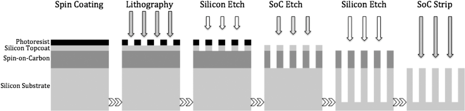
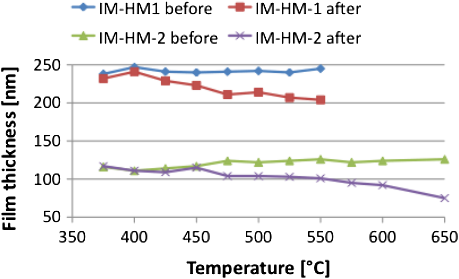
1.IntroductionWith the progress in lithography technology, the feature size of electronic devices continues to shrink further and further. However, in order to achieve the required resolution, the adoption of thinner photoresist films has become necessary to minimize the impact of problems such as pattern collapse of resist features upon development due to aspect ratio.1 A consequence of the reduced resist thickness is the limited aspect ratio in pattern transfer by etching because of the reduced mask durability. We have previously shown that aspect ratios in excess of for 25-nm-halfpitch features are achievable2 using a high-etch-durability, high-resolution,3 fullerene-based resist. However, with the advent of new three-dimensional technologies such as FinFET or Trigate FET, the problem is further exacerbated.4 Using a multilayer hardmask stack to provide the desired aspect ratio at the required resolution can circumvent this issue. The stack comprises alternating layers of materials with differing etch selectivities. A commonly used stack is a thick amorphous carbon layer deposited by chemical vapor deposition topped by a thin silicon-rich layer.5,6 A thin photoresist film is then sufficient to pattern the thin silicon layer, avoiding the pattern collapse problem in thicker resist films. The silicon is then used as a hardmask to pattern the thick carbon layer, giving a high-aspect-ratio carbon pattern suitable for subsequent etching of the silicon wafer. For improved manufacturability and to decrease costs, it is beneficial to replace the use of chemical vapor deposition with spin-on hardmasks (both silicon and carbon).7,8 We have previously introduced a family of fullerene-based “spin-on carbons” (SoCs) with high etch durability and resolution.9–11 These materials have low levels of aliphatic hydrogen, which has been proposed as a solution to “wiggling” of lines during transfer to the thick carbon layer.12 We report here on further characterization of one of the original SoCs thermally and mechanically (IM-HM11-01), and on a new variant SoC (IM-HM12-01), which has been designed to improve the solubility in industry-friendly solvents such as cyclohexanone by modification of the functionalization of the fullerene molecule. 2.Experimental MethodsSample preparation was the same in all cases. Silicon substrates of were prepared by dicing a 100-mm n-type silicon wafer (Rockwood Electronic Materials, Rousset, France) using a Disco DAD 321 wafer dicer. A precut on the back allowed for further separation into pieces after spin coating. The substrates were cleaned using semiconductor-grade chemicals (Puranal). After dicing, the substrates were immersed in isopropyl alcohol (IPA) and placed in an ultrasonic bath for 10 min. The samples were then rinsed in flowing deionized (DI) water for 1 min (Purite Neptune, ) before being immersed in freshly prepared (30%) [] for 10 min. After another 1-min rinse in flowing DI water, the substrates were dipped for 3 min in a weak aqueous solution of HCl (0.1–1%) to form a hydrophobic surface, and finally a further 1-min rinse in flowing DI water. They were then dried with nitrogen and used immediately for SoC film preparation. We evaluated two SoC hardmask compositions from Irresistible Materials. IM-HM11-01 and IM-HM12-01 are formulated with the same crosslinker, but the latter features a new fullerene designed for improved solubility in industrially compatible casting solvents. Solutions were prepared by dissolving appropriate fullerene derivatives in cyclohexanone or anisole with concentrations in the range . The crosslinker was then added at a ratio by weight. The solution was filtered with a 0.02-μm Teflon syringe filter to remove agglomerates. SoC films were produced by spin coating on silicon, at 1000 rpm for 60 s. After coating, the films were baked at a temperature of 300°C for 5 min to render the film insoluble. The solvent compatibility (elution) of the SoC films was determined by measuring the film thickness with a surface profiler (Dektak 3st Auto) before and after a 1-min dip in various solvents followed by a rinse in IPA. Thermal stability was investigated by placing the films in a furnace under nitrogen atmosphere for 5 min and comparing the film thickness before and after heating. Surface roughness was measured with a NanoWizard II atomic force microscope (JPK Instruments, UK) operating in intermittent contact mode employing pyramidal-tipped Si cantilevers (PPP-NCL, Windsor Scientific, UK). Young modulus and hardness were determined by performing nanoindentation on 1-μm-thick films produced by coating multiple successive layers. For etch tests, after preparation of the carbon films, a thin silicon layer was deposited on top by sputter coating at argon pressure with an radio frequency (RF) power of 250 W. After the deposition of the thin silicon layer, photoresist was spin coated onto the sample. A number of different resists have been successfully tested in this application including SAL601 (Shipley), our in-house fullerene-based chemically amplified molecular resist,2,3 and, as used for the work presented here, a non-chemically amplified triphenylene derivative molecular resist.13 Resist patterning was done with a FEI XL30 SFEG scanning electron microscope equipped with an ELPHY Plus pattern generator (Raith GmbH, Dortmund, Germany). Isolated lines and dense line/spaces with linewidths from 20 to 40 nm were written at a beam voltage of 30 keV. All etching was performed using an Oxford Instruments PlasmaPro NGP80 inductively coupled plasma (ICP) system. An overview of the process is shown in Fig. 1. Silicon substrates were attached to a sacrificial silicon wafer using heat sink paste to ensure good thermal contact. The sacrificial wafer was mechanically clamped to the lower electrode, which was equipped with helium backside pressure to ensure good thermal control of the sample during the etching process. The system contained two separately controlled radio frequency power sources supplying 13.6 MHz power to the ICP coil (referred to herein as ICP power) and to the lower electrode (RF power). The ICP power was used to ionize the process gases to generate a high-density plasma, while the RF power was used to allow the DC self bias, and hence the ion energy at the sample, to be controlled independently of the ion density. In the first etch step, the photoresist pattern was transferred into the silicon topcoat by a mixed-mode etch with an flow rate of 25 sccm, flow rate of 30 sccm, RF power of 20 W and ICP power of 220 W, 15 mTorr chamber pressure, 10 Torr helium backing, and stage temperature 5°C. The patterned silicon then acted as etch mask during oxygen plasma etching of the SoC layer with an flow rate of 10–15 sccm, RF power of 150 W and ICP power of 300 W, 2 mTorr chamber pressure, 5 Torr helium backing, and stage temperature 5°C. The final etch step consisted of transferring the carbon hardmask pattern into the silicon substrate by either a mixed-mode etch again or the use of a process chemistry. Conditions for the mixed-mode etch were flow rate of 20 sccm, flow rate of 30 sccm, RF power of 20 W and ICP power of 220 W, 15 mTorr chamber pressure, 10 Torr helium backing, and stage temperature 5°C. plasma conditions were flow rate of 15 sccm, flow rate of 50 sccm, RF power of 20 W and ICP power of 200 W, 20 mTorr chamber pressure, 10 Torr helium backing, and stage temperature 5°C. Etched features were imaged with the SEM in top view and under 45-deg tilt. 3.Results3.1.Film Preparation and CharacterizationThe difference in the two film compositions is in the number of functional adducts. While IM-HM11-01 contains a mono-adduct, the fullerene in IM-HM12-01 is a bis-adduct. The mono-adduct variant from the previous work9–11 required the use of the halogenated solvent chloroform to achieve substantial film thicknesses. However, chloroform is not an industry-acceptable solvent. The aim was therefore to increase the solubility in acceptable solvents in order to spin -thick films. The first solvent tested was anisole. The solubility of the mono-adduct was , and for the bis-adduct. However, after addition of crosslinker, spin coating from this solvent gave a maximum thickness of 75 nm, which is below our desired value of at least 100 nm. In cyclohexanone the solubility of the mono-adduct was , but this increased to in the bis-functionalized fullerene. With concentration it was possible to coat a 4-inch wafer with a defect free -thick SoC film after formulation with the crosslinker. While anisole and cyclohexanone have similar evaporation rates, the viscosity of cyclohexanone is twice that of anisole which probably leads to the higher film thickness. Both compositions have been characterized with respect to their thermal and mechanical properties to determine if the number of adducts has any influence on these parameters. The result from the assessment of the thermal stability is shown in Fig. 2. The increase in adduct number actually seems to be beneficial for the thermal stability as the temperature before the onset of film loss is raised from 400°C to 450°C. Further, the film loss for IM-HM12-01 plateaus after the initial loss at 450°C, until the temperature is in excess of 550°C, which could be indicative of film compaction rather then sublimation and possibly extend the usable temperature range above 450°C for this material. A possible explanation for the higher temperature stability is improved crosslinking as the bis-adduct provides additional crosslinking site in comparison to the mono-adduct. The surface roughness for the two compositions was found to be of comparable size as well as being similar to a reference measurement of the silicon used for the substrate. This demonstrates that the use of the hardmask does not introduce significant roughness (see Fig. 3, Table 1). Measurement of the mechanical parameters, hardness, and Young modulus displayed no significant differences between the two materials. Fig. 3AFM surface roughness of bare silicon (a), IM-HM11-01 (b) (note different scale), and IM-HM12-01 (c). 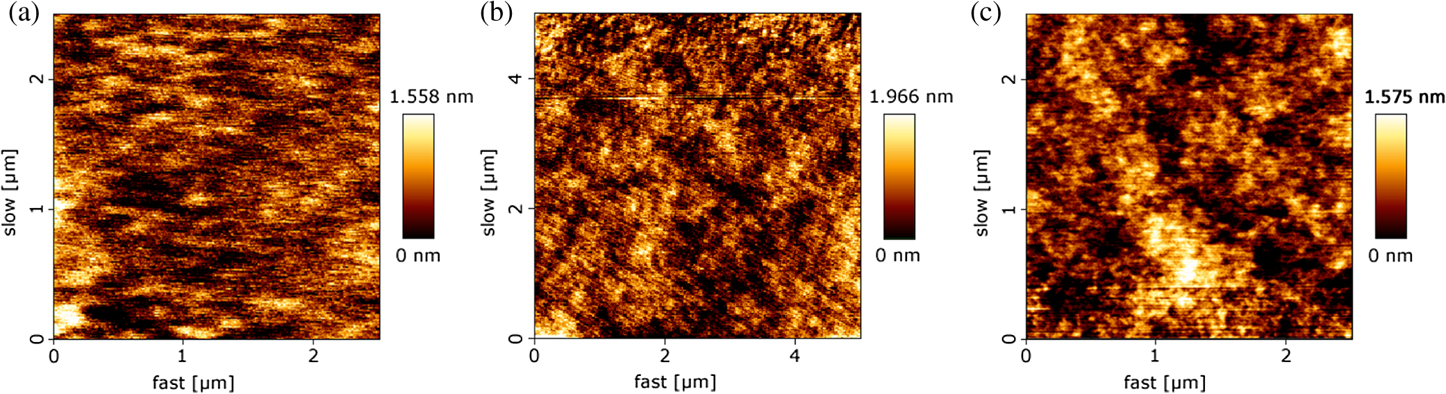 Table 1Comparison of etch rate and selectivity between IM-HM11-01 and IM-HM12-01.
Testing for solvent compatibility (elution) showed that once they had received a postcoating bake, neither material showed measurable film loss or swelling after 1 min of immersion in the following commonly used solvents: propylene glycol monomethyl ether (-acetate), ethyl lactate, ethyl ethoxy propionate, anisole, cyclohexanone, and tetramethylammonium hydroxide (25%), making the material compatible with standard industry processes. 3.2.Hardmask and Silicon EtchingFor comparison of the etch rate and selectivity 10-μm-wide lines were patterned into the hardmask. In addition, the same pattern was written into -thick SAL601 resist film as a control and reference. Samples were etched for 45 s in and plasmas and the feature height recorded before and after silicon etching. After stripping of the remaining resist and SoC material via oxygen plasma ashing, the height of the etched silicon features was measured as well. In this way the amount of SoC masking material removed was calculated. The results are summarized in Table 2. It can be seen that the etch rate of the higher-adduct SoC IM-HM12-01 is lower than that of IM-HM11-01, although it can also be seen that both materials perform better than the SAL601 control—a high-durability novolac resist that has been widely used in microfabrication because of its good etch resistance and resolution. Based on the concept of Ohnishi number,14 which states that the etch rate is proportional to carbon content in the material, we expected the mono-adduct to perform better then the bis-adduct. Calculating the number for both materials gives a value of 1.25 for IM-HM11-01, whereas IM-HM12-01 has a number of 1.45. A lower Ohnishi number typically equates to a lower etch rate. But here we observed that IM-HM12-01 actually showed a lower etch rate. We presume this to be caused by increased crosslinking of the material due to the second adduct. Table 2AFM and Nanoindenter measurements of the IM-HM11-01 and IM-HM12-01 films.
Both IM materials are capable of high-resolution patterning. Examples of the patterned hardmask and transfer into silicon are shown in Fig. 4. Sparse line features with a width of 20 nm were successfully etched into silicon as well as 30-nm dense patterns for both materials. While the plasma chemistry generally does not affect the etch rate of the SoC material, higher aspect ratios are achieved with as the higher silicon etch rate for this gas combination results in a higher etch selectivity. 4.ConclusionIn summary, we have presented material characterization for a previously introduced SoC hardmask and a new variant. With the aim of improving the solubility of the material in industry-accepted solvents, we have further investigated how the material properties change when modifications to the number of functional groups are made. The change in adduct number greatly improved the solubility of the compound in, for example, cyclohexanone. Both the original and modified versions perform better than the SAL601 control resist, although the modified composition had slightly higher etch rate than the mono-adduct variant. Both SoC carbon films were capable of transferring high-resolution features into silicon with high aspect ratio. AcknowledgmentsThe authors thank the Engineering and Physical Sciences Research Council (EPSRC) for support of this project. The Disco DAD 321 wafer dicer and the Oxford Instruments PlasmaPro NGP80 Inductively Coupled Plasma etching system used in this research were obtained through Birmingham Science City: Creating and Characterising Next Generation Advanced Materials, with support from Advantage West Midlands (AWM) and partly funded by the European Regional Development Fund (ERDF). The Atomic Force Microscope and Nanoindenter used in this research were obtained through Birmingham Science City: Innovative Uses for Advanced Materials in the Modern World (West Midlands Centre for Advanced Materials Project 2), with support from AWM and partly funded by the ERDF. We thank Dr. J. Bowen for his assistance with AFM and Young modulus measurements. ReferencesW.-M. Yehet al.,
“A study of reactive adhesion promoters and their ability to mitigate pattern collapse in thin film lithography,”
Proc. SPIE, 7972 79721Y
(2011). http://dx.doi.org/10.1117/12.895112 PSISDG 0277-786X Google Scholar
F. P. Gibbonset al.,
“Fullerene resist materials for the 32 nm node and beyond,”
Adv. Funct. Mater., 18
(13), 1977
–1982
(2008). http://dx.doi.org/10.1002/adfm.v18:13 AFMDC6 1616-3028 Google Scholar
J. Manyamet al.,
“Plasma etching of high-resolution features in a fullerene molecular resist,”
Proc. SPIE, 7972 79722N
(2011). http://dx.doi.org/10.1117/12.879469 PSISDG 0277-786X Google Scholar
T. Vandeweyeret al.,
“Patterning challenges in setting up a 16 nm node 6T-SRAM device using EUV lithography,”
Proc. SPIE, 7969 79691K
(2011). http://dx.doi.org/10.1117/12.881690 PSISDG 0277-786X Google Scholar
S. Pauliac-Vaujouret al.,
“Improvement of high resolution lithography by using amorphous carbon hard mask,”
Microelectron. Eng., 85
(5–6), 800
–804
(2008). http://dx.doi.org/10.1016/j.mee.2008.02.007 MIENEF 0167-9317 Google Scholar
C.-Y. Hoet al.,
“High aspect ratio contact hole etching using relatively transparent amorphous carbon hard mask deposited from propylene,”
Thin Solid Films, 518
(21), 6076
–6079
(2010). http://dx.doi.org/10.1016/j.tsf.2010.06.008 THSFAP 0040-6090 Google Scholar
Z. Zhuet al.,
“Thin hardmask patterning stacks for the 22-nm node,”
Proc. SPIE, 7274 72742K
(2009). http://dx.doi.org/10.1117/12.813816 PSISDG 0277-786X Google Scholar
Y. Weiet al.,
“Performance of tri-layer process required for 22 nm and beyond,”
Proc. SPIE, 7972 79722L
(2011). http://dx.doi.org/10.1117/12.879301 PSISDG 0277-786X Google Scholar
A. Frommholdet al.,
“High aspect ratio etching using a fullerene derivative spin-on-carbon hardmask,”
Proc. SPIE, 8328 8328U
(2012). http://dx.doi.org/10.1117/12.916426 PSISDG 0277-786X Google Scholar
A. Frommholdet al.,
“Fullerene-based spin-on-carbon hardmask,”
Microelectron. Eng., 98 552
–555
(2012). http://dx.doi.org/10.1016/j.mee.2012.07.019 MIENEF 0167-9317 Google Scholar
A. Frommholdet al.,
“Chemically amplified fullerene resists, spin-on fullerene hardmasks and high aspect ratio etching,”
in 12th IEEE Conference On Nanotechnology (IEEE-NANO),
(2012). Google Scholar
M. Gloddeet al.,
“Systematic studies on reactive ion etch-induced deformations of organic underlayers,”
Proc. SPIE, 7972 797216
(2011). http://dx.doi.org/10.1117/12.879442 PSISDG 0277-786X Google Scholar
T. Tadaet al.,
“A triphenylene derivative as a novel negative/positive tone resist of 10 nanometer resolution,”
Microelectron. Eng., 53
(1–4), 425
–428
(2000). http://dx.doi.org/10.1016/S0167-9317(00)00348-8 Google Scholar
H. GokanS. EshoY. Ohnishi,
“Dry etch resistance of organic materials,”
J. Electrochem. Soc., 130
(1), 143
–146
(1983). http://dx.doi.org/10.1149/1.2119642 JESOAN 0013-4651 Google Scholar
Biography Andreas Frommhold graduated from the Ilmenau University of Technology with a Dipl. Ing. degree in electrical engineering in 2000. He obtained his PhD in electrical engineering in 2010, for work on nanostructure modification of neural implants, at the University of Birmingham. He is currently a research fellow in the School of Chemical Engineering at the University of Birmingham. His research interests include chemically amplified molecular resists for electron beam and EUV lithography, as well as the development of nanomaterials for micro- and nanofabrication and plasma etching.  Richard E. Palmer is professor of experimental physics at the University of Birmingham and head of the Nanoscale Physics Research Laboratory. His research interests include atomic clusters, biochips, atomic manipulation, and nanofabrication. He obtained his first degree (1983) and PhD (1986) at Cambridge University, where he held 1851, Clare College, and Royal Society Research Fellowships. He has held visiting positions at Cornell, Oxford, and Harvard Universities and the Technical University of Denmark. He has been elected to honorary professorships at the University of Wales, Swansea, Harbin Institute of Technology, China, and the Petronas University of Technology, Malaysia. He was awarded an honorary doctoral degree by Hasselt University, Belgium, in 2010 “for his pioneering work in nanoscale physics and his contributions to bridging the gap between nanoscience and nanotechnology.” In 2012, he was elected fellow of the Royal Society of Chemistry and won a senior EPSRC Fellowship.  Alex P. G. Robinson is a senior research fellow of the Science City Research Alliance at the Universities of Birmingham and Warwick. He obtained his PhD in 2000 for work on molecular resist materials done in the Nanoscale Physics Research Laboratory at University of Birmingham, and the Joint Research Center for Atom Technology in Japan. His research interests have included modification of oxide surfaces using self assembled mono- and multilayers, coaxial field emission tips, nanostructured biosensors and bio interface surfaces, and resist properties of amorphous low molecular weight materials, low energy electron beam resists, chemically amplified molecular resists for electron beam and EUV lithography, and ICP etching. |