
|
|
1.IntroductionThe controlled fabrication of surface topography—with nanoscale patterns more intricate than square-edged channels or gratings—has seen a recent rise in interest.1 In particular, controlled patterning of surfaces with limited, 2.5-dimensional (2.5-D) (for patterns with periodicity in the illumination plane) or complete [fully three-dimensional (3-D)] pattern variation normal to the wafer surface has seen increased demand.2 These structures find application in propagating plasmon-mode biosensors3–6 and assays that can control protein7 or block copolymer8 absorption. However, no general and parallel fabrication technique has emerged to fill this need. Focused ion beam sputtering is well known;9 however, it presents clear integration difficulties since it is a serial, scanned-beam process. Conformal phase masks have been used to fabricate micron-thick layers with intricate 3-D structure,10,11 yet are not capable of patterning a surface layer without first patterning the mask itself, and without taking advantage of an optical reduction factor. Interference lithography12 limits the feature size to between and , placing severe constraints on final dimensions of devices made with conventional tools. Recent developments in spatially controlled deposition kinetics13 are promising, but limit materials and geometry. Grayscale14 and multilayer techniques15 limit feature sizes as well, and require expensive single mask or multiple mask sets. In this work, a fabrication approach that does not suffer from these difficulties is presented. By controlling not just the exposure dose delivered, but also the illumination profile in the photoresist (the aerial image), periodic structures with a wide variety of profiles are fabricated. These structures are created using off-the-shelf hardware, operating with well-understood -line illumination () and with commercially available photoresists, and modeling the exposure with commercially supported codes. Examples of using this technique to fabricate structures with variation in size and curvature are demonstrated. Moreover, the approach is generalized not only to the fabrication of structures in photoresist, but also the etch transfer of those structures to an underlayer. This is accomplished by control of the aerial image; by modulating the exposure dose delivered, the image focus, and the postexposure conditions:16 the postexposure bake, spray development, and hard bake. The modified mask feature spacing controls the interaction between the focal plane and the aerial image; the dose and focus modulations change the absorbed axial image, and the development parameters control the kinetics of the development. Each of these can be simulated numerically to sufficient precision to reliably produce the desired 2.5-D pattern. 2.Experiments and MethodsTo develop an appropriate test structure, full-field finite-difference time domain (FDTD) simulations were performed in Lumerical FDTD. The desired image plane intensity was simulated with the PROLITH lithography simulation package, by KLA-Tencor. The design space under consideration consists of devices with sinusoidal or smoothly curved sidewall profiles, as depicted in Fig. 1. With a specific design in mind, PROLITH was used to calculate the desired photoresist image, taking into account the photoresist and anti-reflection layers, the substrate materials and variation in sidewall profile. The material parameters used came exclusively from the PROLITH database, with the exception of the data for the SPR-220 resist, which was supplied by the manufacturer. Having established a materials stack, iterations were performed over physically controllable inputs—the focus plane and optical dose delivered—to determine the experimental parameters. Fig. 1Overlays of the developed results against the PROLITH simulation target for a number of designs. From left to right, the dose increases from 50 to ; from bottom to top, the focus offset (measured toward the optical system) increases from to 0.3 μm. The PROLITH simulation yields the expected sinusoidal pattern with a reasonable fabrication window; perturbations around the best achievable value degrade the aerial image variation. 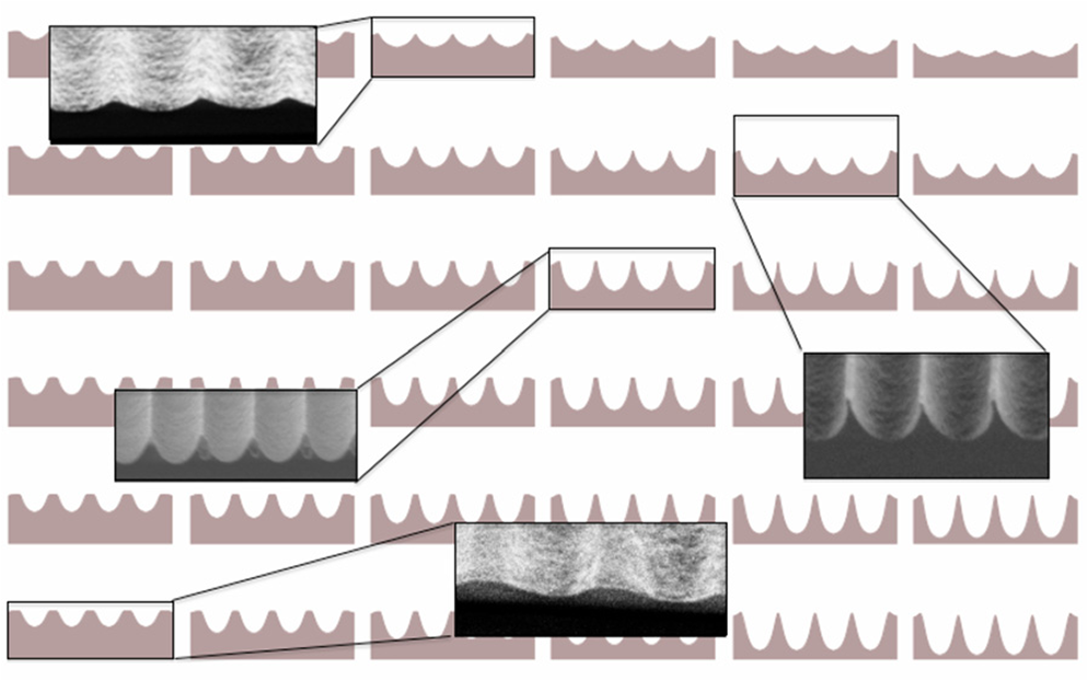 To verify these results experimentally, the appropriate photoresist thickness for the design feature size and depth was calculated. Typically, the simulation optical stack consists of a constant 165 nm layer of Brewer Science XHRi-16c anti-reflective coating (ARC) beneath the Megaposit SPR-220 photoresist, with a thickness of . A line-space grating of 400 nm lines with 500 nm spaces was used, operating at the linear resolution limit of -line lithography. This mask was used to fabricate metal-dielectric structures in which plasmon resonances, discussed below, were observed. Bare silicon wafers (with Miller indices ) were coated with the photoresist stack. Manufacturer suggested solvent bake times for each layer were used; in the case of SPR-220: 90°C for 60 s. The wafers were exposed using a GCA Autostep 200 -line wafer stepper, using a numerical aperture of 0.45 (). The tool dose was verified before each batch: values of are typical, corresponding to exposure times of . A combined focus-exposure matrix, with focus offset values suggested by simulation, was developed to optimize exposure; each die was exposed once. Depending on desired geometry, focus offset values were between 300 nm and 1.5 μm. Wafers were then postbaked and developed in accordance with simulated parameters, with typical values near the manufacturer suggestions for postbake ( for 60 s on hot-plate) and spray developed for 60 s in AZ 726 MIF. Having developed the optical process, an etch process was developed17 to transfer the resultant sinusoidal geometry into the underlayer: in this case, the bulk silicon wafer. A reactive ion etch process was used, with as the etchant and to increase selectivity to photoresist, in a flow ratio. The forward power was 150 W and the chamber pressure was 40 mtorr. The reflectivity, at variable angle of incidence, was characterized by an optical setup contained a tungsten–halogen source, Horiba iHR550 infrared monochromator, collimating silver mirror, polarizing prism, focusing silver mirror, and silicon photodetector. The measurements were performed using a linearly polarized collimated beam with a spectral range spanning 400 to 1100 nm. Collected data was normalized against the reflection of a flat silver mirror. 3.Results and Discussion3.1.Exposure SimulationsThe PROLITH simulation yields the expected sinusoidal pattern with a reasonable fabrication window; perturbations around the best achievable value degrade the aerial image quality linearly and controllably. Physical inputs of reasonable photoresist and ARC layers, reasonable mask sizes and development times yield a variety of sinusoidal patterns; thus, there is an acceptable tolerance in process and equipment variation. Iterations over the line and space width of the mask yielded changes in the structure size while still operating in the near-field approximation. Beyond , the simulated exposures converged back to near-vertical sidewall profiles, as expected. The region of interest in this work remains with mask feature sizes approaching the illumination wavelength. Iterations over the dose begin from half the typical value expected for full exposure; iterations for focus begin from , where is the thickness of the optical stack— for the example developed here. This coarse iterative simulation elucidates typical behavior for a photoresist stack; the photoresist profile is then fine-tuned by iterating predominantly over dose close to the desired profile. Moreover, multiple exposures, at varying focal planes, were considered in simulation. These enabled additional parameters to capture a broader array of exposure profiles at the expense of alignment accuracy and multipass exposure. The criteria used to judge the success of the simulations were the fidelity of the output to the intended geometry of the structure: the top CD size, bottom CD size, pattern height, space width, pattern curvature were taken into consideration. It is important to underscore that the values discussed above are all approximate, and should be used as reasonable initial setting for subsequent experiments. For a given process target, accurate and exact values are produced by running a full simulation against the desired geometry. Modulation of dose and mask linewidth can be used as coarse adjustments to the eventual geometry, while focus offset acts as a much more sensitive perturbation. 3.2.Photoresist Patterning, Etch TransferPatterning photoresist using this technique yields a variety of controlled cross sectional profiles. Figure 2 shows a scanning electron microscopy (SEM) cross section of photoresist, exposed and developed according to a simulation tailored toward a sinusoidal image. The subfigures demonstrate other geometries that can be created with the above technique, similarly in photoresist. An asymmetrical grating is shown with a curved base and sharper tops. Moreover, a more extreme example is developed: an array of sharply tipped lines. Fig. 2A scanning electron microscopy (SEM) image of patterned photoresist using the controlled defocus lithography technique emphasizing the variety of producible patterns. An extreme example of aerial image modulation is visible in inset (a). Inset (b) is an edge-on sine wave pattern. Finally, we see an interim example of the possible gradation in inset (c). 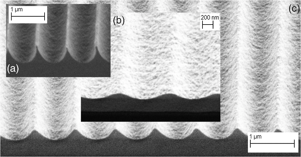 Multiple iterations of this process yield reliable pattern generation and transfer, as demonstrated in Fig. 1. Using a dose–focus matrix for optimization, patterns that compare closely to those generated in simulations are produced. While creating patterns in photoresist is useful, far greater utility lies in transferring these to underlayers and enabling deposition of a coating. In Fig. 3, the transfer of the photoresist pattern into the silicon substrate is demonstrated, along with a gold coating. Using the etch parameters described above, etch selectivity within 7% of unity is achieved, yielding minimal change in the photoresist aspect ratio. Fig. 3An edge-on () SEM image of a periodic pattern transferred into the substrate, and coated in 25 nm gold. The photoresist pattern, here, is taken from the sample shown in Fig. 2(c). 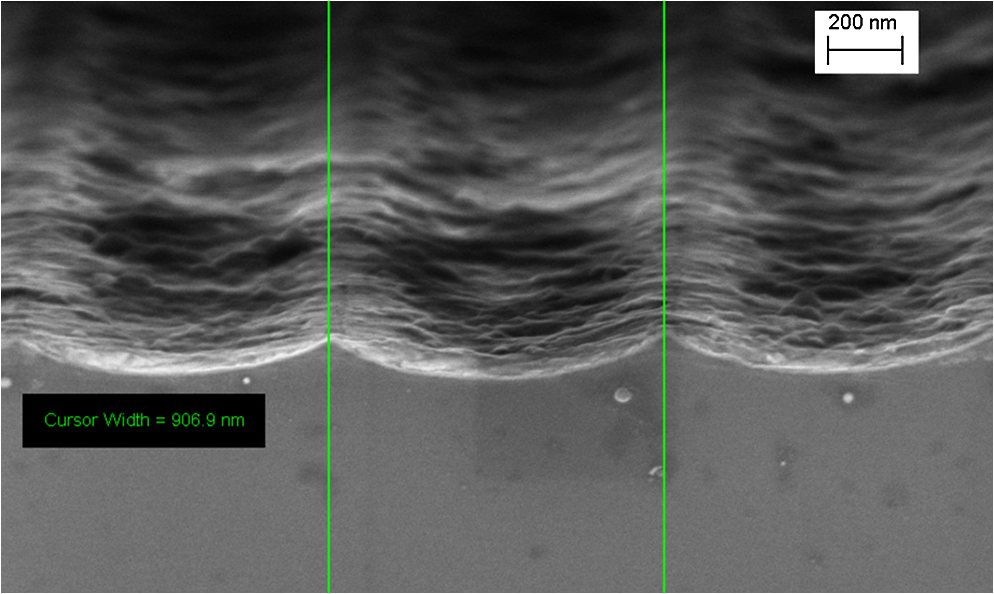 3.3.Narrowband Plasmon ResonanceWe used this approach to construct a surface plasmon-based asymmetrical grating, with a decreased density of plasmon states near the grating edge, yielding particularly narrowband performance. Reflection spectra calculated by FDTD simulation are compared to experimental measurements. The reflectivity of the metal-dielectric sample in Fig. 3 was measured using normal incident angle of transverse magnetic polarized probing light, and is presented in Fig. 4. Fig. 4The measured -polarized spectral reflectance (points), with the simulated spectral reluctance (solid curve), at normal incidence. The measured reflection minimum is at 911 nm, whereas the calculated reflection minimum is at 909 nm. This resonance is due to optical excitation of propagating plasmon modes along with the asymmetric curved surface. Below , diffraction losses decrease directional reflectivity. 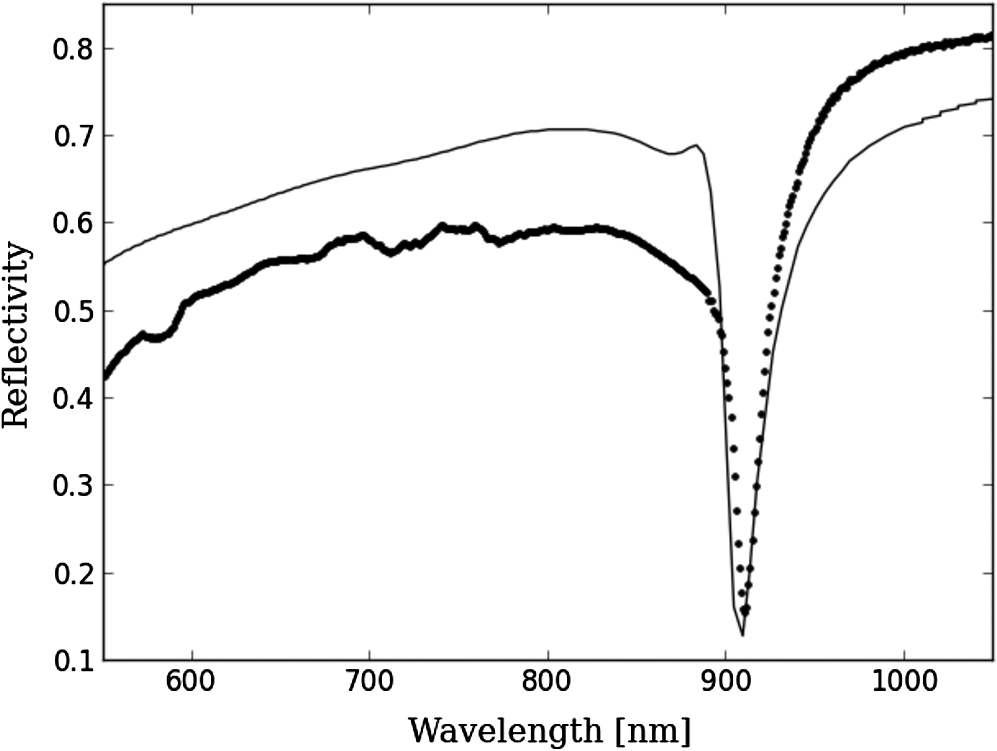 The peaks, each indicating the incident illumination coupling into a surface mode, overlap to within . The sample demonstrated a narrow-band reflectivity minimum for the -polarized probe field at the wavelength of 911 nm (Fig. 4). The minimum wavelength was blue-shifted with increasing angle of incidence. In contrast, the reflection of -polarized light did not demonstrate any minimum of reflectivity at 911 nm or any other wavelength within the measurement range. The resonance is narrow, with a full-width at half-maximum of 19 nm, indicating a high-quality periodic structure. 4.ConclusionAbove, the fabrication of 2.5-D periodic structures using a one-step optical lithography process compatible with conventional -line tools is demonstrated. Etch transfer of the shape, with high fidelity, into the underlying silicon is performed. Limitations of this technique became evident during the development of this process. Image fidelity is affected by focus control. Moreover, technology transfer to industrial processes, using 200 mm substrates and with decreased tolerances for resist uniformity and wafer bow, may be challenging. While this approach has been implemented before using electron-beam lithography,18 an approach using photolithography enables integration with a parallel workflow, and a reduction in fabrication cost. In the realm of all-optical techniques, the aerial image modulation approach enables topography patterning of feature sizes too large for holographic lithography and too small for grayscale approaches. AcknowledgmentsThis work was performed in part at the Cornell NanoScale Science and Technology Facility, a member of the National Nanotechnology Infrastructure Network, which is supported by the National Science Foundation (Grant No. ECS-0335765). We thank Meredith Metzler and Vince Genova for insight and assistance with the etch transfer development. ReferencesM. WatanabeK. Mizukami,
“Well-ordered wrinkling patterns on chemically oxidized poly(dimethylsiloxane) surfaces,”
Macromolecules, 45
(17), 7128
–7134
(2012). http://dx.doi.org/10.1021/ma301143m MAMOBX 0024-9297 Google Scholar
Y. Fuchset al.,
“Holographic molecularly imprinted polymers for label-free chemical sensing,”
Adv. Mater., 25
(4), 566
–570
(2012). http://dx.doi.org/10.1002/adma.201370025 ADVMEW 0935-9648 Google Scholar
B. FischerT. M. FischerW. Knoll,
“Dispersion of surface plasmons in rectangular, sinusoidal, and incoherent silver gratings,”
J. Appl. Phys., 75
(3), 1577
–1581
(1994). http://dx.doi.org/10.1063/1.356394 JAPIAU 0021-8979 Google Scholar
S. C. Kitsonet al.,
“Surface profile dependence of surface plasmon band gaps on metallic gratings,”
J. Appl. Phys., 79
(9), 7383
(1996). http://dx.doi.org/10.1063/1.361456 JAPIAU 0021-8979 Google Scholar
R. A. WattsT. PreistJ. R. Sambles,
“Sharp surface-plasmon resonances on deep diffraction gratings,”
Phys. Rev. Lett., 79
(20), 3978
–3981
(1997). http://dx.doi.org/10.1103/PhysRevLett.79.3978 PRLTAO 0031-9007 Google Scholar
R. A. WattsA. P. HibbinsJ. R. Sambles,
“The influence of grating profile on surface plasmon polariton resonances recorded in different diffracted orders,”
J. Mod. Opt., 46
(15), 2157
–2186
(1999). http://dx.doi.org/10.1080/09500349908231399 JMOPEW 0950-0340 Google Scholar
M. KurylowiczM. GiulianiJ. R. Dutcher,
“Using nanoscale substrate curvature to control the dimerization of a surface-bound protein,”
ACS Nano, 6
(12), 10571
–10580
(2012). http://dx.doi.org/10.1021/nn302948d 1936-0851 Google Scholar
K. Aissouet al.,
“Nanoscale block copolymer ordering induced by visible interferometric micropatterning: a route towards large scale block copolymer 2D crystals,”
Adv. Mater., 25
(2), 213
–217
(2012). http://dx.doi.org/10.1002/adma.201203254 ADVMEW 0935-9648 Google Scholar
Y.-Z. Huanget al.,
“Rapid fabrication of nanoneedle arrays by ion sputtering,”
Nanotechnology, 19
(1), 015303
(2008). http://dx.doi.org/10.1088/0957-4484/19/01/015303 NNOTER 0957-4484 Google Scholar
M. C. Georgeet al.,
“Direct fabrication of 3D periodic inorganic microstructures using conformal phase masks,”
Angew. Chem., Int. Ed., 48
(1), 144
–148
(2009). Google Scholar
D. Shiret al.,
“Three dimensional silicon photonic crystals fabricated by two photon phase mask lithography,”
Appl. Phys. Lett., 94
(1), 011101
(2009). http://dx.doi.org/10.1063/1.3036955 APPLAB 0003-6951 Google Scholar
J. K. ChuaV. M. Murukeshan,
“Patterning of two-dimensional nanoscale features using grating-based multiple beams interference lithography,”
Phys. Scr., 80
(1), 015401
(2009). http://dx.doi.org/10.1088/0031-8949/80/01/015401 PHSTBO 0031-8949 Google Scholar
M. Luet al.,
“Single-step holographic fabrication of large-area periodically corrugated metal films,”
J. Appl. Phys., 112
(11), 113101
(2012). http://dx.doi.org/10.1063/1.4768201 JAPIAU 0021-8979 Google Scholar
L. Mosheret al.,
“Double-exposure grayscale photolithography,”
J. Microelectromech. Syst., 18
(2), 308
–315
(2009). http://dx.doi.org/10.1109/JMEMS.2008.2011703 JMIYET 1057-7157 Google Scholar
A. Zebdaet al.,
“Spin coating and plasma process for 2.5D integrated photonics on multilayer polymers,”
Thin Solid Films, 516
(23), 8668
–8674
(2008). http://dx.doi.org/10.1016/j.tsf.2008.04.095 THSFAP 0040-6090 Google Scholar
C. A. Mack,
“Understanding focus effects in submicrometer optical lithography: a review,”
Opt. Eng., 32
(10), 2350
–2362
(1993). http://dx.doi.org/10.1117/12.146837 OPEGAR 0091-3286 Google Scholar
J. KimD. C. JoyS.-Y. Lee,
“Controlling photoresist thickness and etch depth for fabrication of 3D structures in electron-beam grayscale lithography,”
Microelectron. Eng., 84
(12), 2859
–2864
(2007). http://dx.doi.org/10.1016/j.mee.2007.02.015 MIENEF 0167-9317 Google Scholar
D. Liuet al.,
“Fabrication of polynomial 3-D nanostructures in Si with a single-step process,”
J. Micro/Nanolithogr. MEMS MOEMS, 10
(1), 010501
(2011). http://dx.doi.org/10.1117/1.3563601 JMMMHG 1932-5150 Google Scholar
Biography Boyan Penkov completed a BS in engineering physics at Cornell University and a MSEE in electrical engineering at the University of Washington before serving as an engineer at an early-stage company seeking to commercialize optical metamaterials. His previous work at the intersection of nanoscience and biology has yielded six journal papers, one patent, and seven peer-reviewed conference contributions. He is currently an NDSEG fellow at the Bioelectronic Systems Lab at Columbia University, and he is pursuing a PhD in electrical engineering under the direction of Kenneth Shepard.  Garry Bordonaro has been a photolithographic process engineer at CNF since 1993. He is experienced in processes using DNQ-Novolak resists in both contact and projection photolithography, and DUV resists and processes using both contact and projection. He is also experienced with CAD design, mask making, simulations using PROLITH X4 by KLA-Tencor, and general semiconductor processing. He is a trainer and lecturer in all of these areas as well. In his spare time, he tours the world as a musician with metal rock bands.  Andrii B. Golovin received his MSE degree in optics and electronics from the Department of Physics, Kiev State University, Ukraine, in 1987. He received his PhD degree in physics and mathematics from the Institute of Physics, Academy of Sciences, Kiev, Ukraine, in 1994. He has conducted research in the areas of laser physics, electro-optics of liquid crystals and metamaterials, and optical engineering. He has been a research professor at the Center for Metamaterials, Research Foundation of City University of New York, since December 2011. His synergetic activities include teaching courses of physics and mathematics at City College of New York (present), Stark State College of Technology (2010 to 2011), Kent State University (2005 to 2008), and National University of Colombia (1999 to 2000). He has received Tech Brief Awards from Inventions and Contributions Board of NASA (2008, 2006), Award of Ukrainian Academy of Sciences (1997), and Award from the Ukrainian Committee on Science and Technology (1996).  Igor Bendoym is principal investigator and lead simulation engineer at Phoebus Opto-electronics. After receiving his BS degree in electrical engineering from CCNY, Mr. Bendoym joined the laboratory of Dr. David Crouse as a senior research associate. He has led several Phoebuss simulation projects, as well as many academic projects in the fields of photonic crystals, antennas, metamaterials, and other optical materials.  Don M. Tennant is serving as director of operations of the Cornell NanoScale Science and Technology Facility (CNF) after a long career at Lucent Bell Labs where he was a distinguished member of technical staff and managed the advanced lithography group. His research work has had significant impact on a wide range of disciplines, including: soft x-ray imaging, extreme ultraviolet lithography (EUVL), high-precision grating production for optical network components, and gate technologies for high performance devices and circuits. He has authored or co-authored over 200 articles in these fields, has organized major conferences, and has been awarded 11 US patents. Don currently serves on the advisory committee and is the financial trustee for the International Conference of Electron, Ion, and Photon Beams and Nanotechnology (EIPBN). He is a past chairman of the Nanoscale Science and Technology Division of the AVS and was named a fellow of the society in 2010.  David T. Crouse is an associate professor in the Department of Electrical Engineering at the City College of New York, director of the National Science Foundation Industry/University Cooperative Research Center for Metamaterials, director of the Center for Advanced Technology in Photonics Applications, and founder of Phoebus Optoelectronics LLC. He received a BS in honors physics from Purdue University in 1997 and a PhD in electrical engineering at Cornell University in 2002. His research interests include fundamental and applied research on plasmonics crystals, metamaterials and nanotechnology. |


