|
|
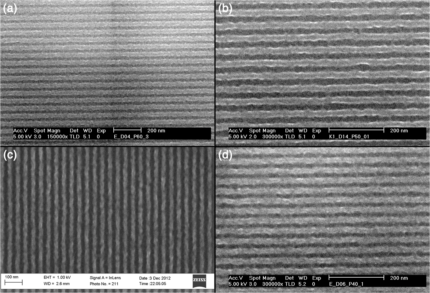
1.IntroductionWith the advancement in next generation lithography (NGL) technology continuing, the progress in patterning capability is increasingly being limited by the lithographic performance of the photoresist. Current lithographic nodes already require line width roughness that is smaller than the radius of gyration of typical resist polymers.1 Further progress in the development of new resists is needed to enable the commercial production of semiconductors at the sizes mapped for the future. Low molecular weight resists, such as fullerenes,2,3 triphenylenes,4,5 molecular glasses,6,7 and inorganic resists,8,9 have been a focus of interest for NGL because their small size promises high resolution and small line edge roughness. But so far, no resist candidate has emerged that fulfills all the industry’s criteria. We have previously reported on the performance of a fullerene derivative based three-component negative tone chemically amplified resist for e-beam lithography with low line edge roughness (LER) and high resolution capability,10,11 and on a positive tone variant of the fullerene resist.12 E-beam resists have often been shown to work in extreme ultraviolet lithography (EUVL) as well because of similarities in the exposure mechanisms in the resist. Therefore, we believe that this resist platform has a great potential for EUVL. Here we present recent results of our investigation into the EUVL performance of a fullerene derivative based resist system.13 2.Experimental MethodsFullerene derivatives for the resist were supplied by Irresistible Materials Ltd., United Kingdom Figure 1(a) shows the tert-butoxycarbonyl (tBOC) protected methyl phenolic malonate derivative (IM-MFPT-12-21), and the tBOC protected propyl phenolic malonate derivative (IM-MFPT-12-8, -12-19, -13-32, -13-33). An epoxy crosslinker (Araldite ECN 1299; Huntsman Advanced Materials, The Woodlands, Texas) [Fig. 1(c)] and triphenylsulfonium hexafluoroantimonate PAG (TPS-103; Midori Kagaku Co., Japan) [Fig. 1(d)] were added. Fig. 1(a) a tert-butoxycarbonyl (tBOC) protected methyl phenolic malonate , (b) a tBOC protected propyl phenolic malonate , (c) epoxy crosslinker, and (d) triphenylsulfonium hexafluoroantimonate photoacid generator. 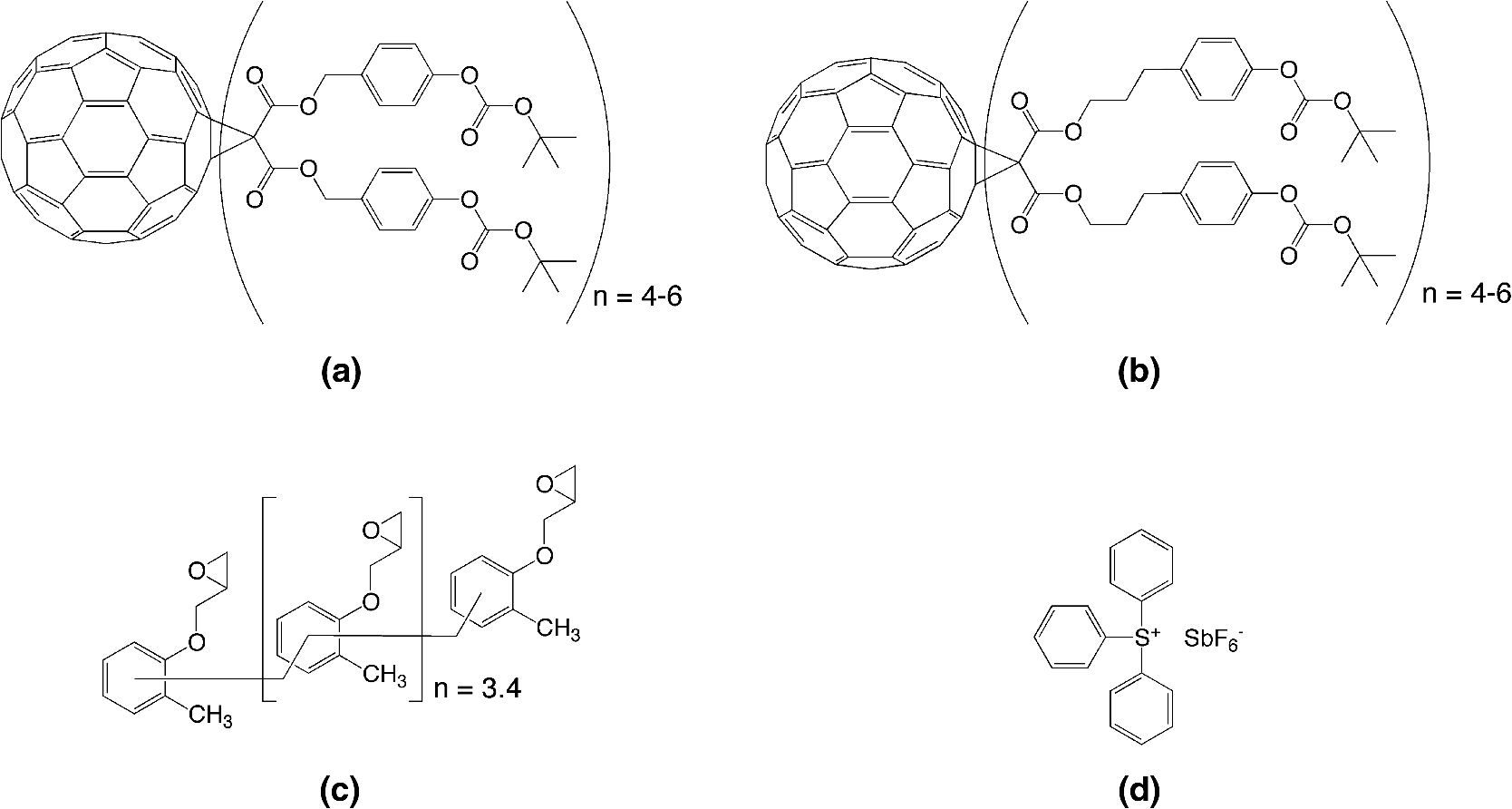 Synthesis of the derivatives was achieved via the modified Bingel14,15 cyclopropanation reaction of a bismalonate ester, with the , to afford the methanofullerenes and is described in depth elsewhere (Yang et al., unpublished). 2.1.IM-MFPT-12-8In a round bottom flask, [60]fullerene (1 equivalent), 9,10-dimethylancethracene (22 equivalent) and toluene were added. The resulting solution was stirred for 1 h to completely dissolve the fullerene. Carbon tetrabromide (22 equivalent) and 3-(4-t-butoxycarbonyl)phenyl-1-propyl malonate (22 equivalents) were added to the solution. 1,8-Diazabicyclo[5.4.0]undec-7-ene (DBU) (108 equivalents) was added dropwise and the resulting mixture was stirred at room temperature overnight and the initial purple solution had become a dark red color. The crude mixture was poured through a silica plug in a sintered glass funnel and rinsed with toluene (4 L) to remove unreacted [60]fullerene and then rinsed with dichloromethane: ethyl acetate:methanol () to remove the red/brown band containing the crude products. The solvents were evaporated and the resulting residue [3-(4-t-butoxycarbonyl)phenyl-1-propyl malonate]-methano-[60]fullerene (dark red/brown oil) was obtained. NMR (300 MHz, CDCl3): to 7.70 (m), 0.9 to 4.1 (m), 1.55 (s). The product was characterized by matrix-assisted laser desorption/ionization mass spectrometry (MALDI MS). Major components were multiadduct fullerenes with to 6. 2.2.IM-MFPT-12-19IM-MFPT-12-19 was synthesized and purified as for IM-MFPT-12-8. The crude mixture was redissolved in methylene chloride at a concentration of and processed by size exclusion chromatography (Phenogel SEC , 5 μm particle size, eluent: methylene chloride, ). The material corresponding to 1000 to 3000 atomic mass unit (AMU) was collected and the solvent was evaporated to obtain a red oil. This material was characterized by MALDI MS. 2.3.IM-MFPT12-21In an 1-L round bottom flask, [60]fullerene (0.85 g, 1.2 mmol), 9,10-dimethylancethracene (2.62 g, 13 mmol, 11 equivalents) and toluene (500 mL) were added. The resulting solution was stirred for 1 h to completely dissolve the fullerene. Carbon tetrabromide (4.78 g, 13 mmol, 11 equivalents) and t-butoxycarbonyl malonate (6.6 g, 13 mmol, 11 equivalents) were added to the solution. DBU (8.3 mL, 53.2 mmol) was added dropwise and the resulting mixture was stirred at room temperature overnight and the initial purple solution had become a dark red color. The crude mixture was poured though a silica gel plug in a sintered glass funnel and rinsed with toluene to remove unreacted [60]fullerene. After that, the plug was rinsed with dichloromethane:ethyl acetate:methanol () to remove the red/brown band containing the crude products. The filtrate was evaporated and the resulting residue was purified via flash column chromatography with dichloromethane:ethyl acetate:methanol as eluent. (t-butoxycarbonyl malonate)-methano-[60]Fullerene (1.8 g, dark red/brown oil) was obtained. The oil was dissolved in methylene chloride at a concentration of and processed by semi-preparative size exclusion chromatography (Phenogel SEC , 5 μm particle size, eluent: methylene chloride, ). The material corresponding to 1000 to 3000 AMU was collected and the solvent was evaporated to obtain a red oil. This material was characterized by MALDI MS. 2.4.IM-MFPT-13-32 and IM-MFPT-13-33They were synthesized for IM-MFPT-12-8. Reaction crude mixture was poured through flash column chromatography using silica gel and washed with toluene to remove unreacted [60]fullerene and then two bands were obtained with different eluents: dichloromethane: ethyl acetate () and dichloromethane:ethyl acetate:methanol (). The solvents were evaporated and the resulting two residues (IM-MFPT-13-32 and IM-MFPT-13-33, dark red/brown oil) were obtained. nuclear magnetic resonance (NMR) (IM-MFPT-13-32, 300 MHz, CDCl3): to 7.70 (m), 0.9 to 4.1 (m), 1.55 (s). NMR (IM-MFPT-13-33, 300 MHz, CDCl3): , 6.90 to 8.70 (m), 0.9 to 4.1 (m), 1.55 (s). The products were also characterized by MALDI MS. Silicon substrates of were prepared by dicing a 100-mm -type, -silicon wafer (Rockwood Electronic Materials, France) using a Disco DAD 321 wafer dicer. The substrates were cleaned using semiconductor grade chemicals (Puranal, Sigma Aldrich). After dicing, the substrates were immersed in isopropyl alcohol (IPA) and placed in an ultrasonic bath for 10 min. The samples were then rinsed in flowing deionized (DI) water for 1 min (Purite Neptune, ) before being immersed in freshly prepared (95% to 98%): (30%) [] for 10 min. After another 1-min rinse in flowing DI water, the substrates were dipped for 3 min in a weak aqueous solution of hydrofluoric acid (0.1% to 1%) to form a hydrophobic surface, and finally a further 1-min rinse in flowing DI water. They were then dried with nitrogen and immediately coated with a fullerene containing underlayer, based on a thinned version of our previously reported spin-on-carbon,16,17 to provide a suitable surface for subsequent resist spinning. Substrates were then packaged in chip holders (Entegris H20) and shipped to the EUV testing facility within 3 days. EUV exposures were performed using the interference lithography tool at the Paul Scherrer Institute (PSI), Switzerland.18 Solutions of resist were formulated at PSI by mixing the fullerene derivative with the crosslinker and photo acid generator at various ratios and concentrations, typically 1 part fullerene to 2 parts crosslinker and 1 part photoacid generator (PAG) by weight, in ethyl lactate or propylene glycol monomethyl ether. No other components (quencher etc.) were added. Resist was spun onto the substrates at 1000 to 2000 rpm for 60 s and received a postapplication bake of 75°C for 5 min. After the exposure, the samples were baked at 90°C for 3 min before being developed in monochlorobenzene (MCB):IPA [] for 20 s followed by rinsing in IPA. Alternative developers, cyclohexanone and 2-heptanone, have also been used successfully, as discussed below. Exposed samples were analyzed with a FEI XL30 SFEG scanning electron microscope (SEM) in top–down view. Critical dimension (CD) and LER were calculated from the SEM images with the commercial software package SuMMIT. Dose at the wafer was calibrated for each exposure run by using a reference resist as detailed elsewhere.16 3.Results and DiscussionsThe exposure of numerous variants of the resist formulation showed that it is capable of high resolution. Examples of resist patterns with half-pitches down to 20 nm are shown in Fig. 2. The corresponding resist metrics are summarized in Table 1. The images suffer somewhat from low contrast, which is due to the necessary thinness of the resist film. We found that for aspect ratios significantly greater than , the resist is prone to pattern collapse at half-pitches . Nevertheless, there is a significant potential for improvement in the process of optimizing the synthesis of the fullerene material towards improvement of mechanical stability to allow for higher aspect ratios. Table 1Resist characteristics at different half-pitch sizes.
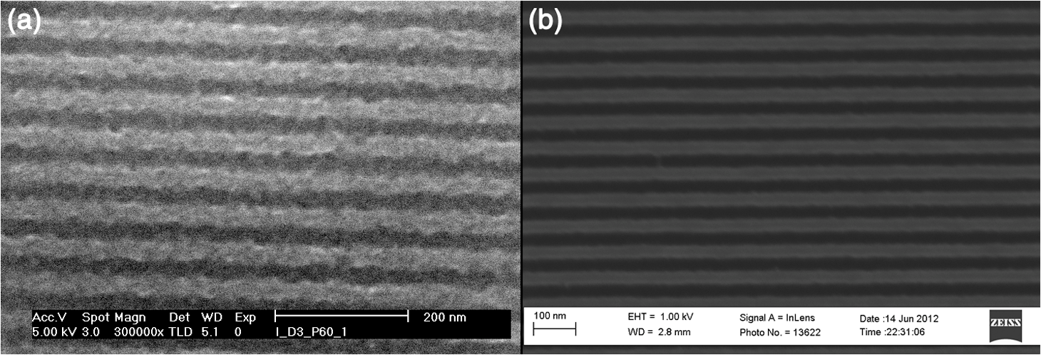
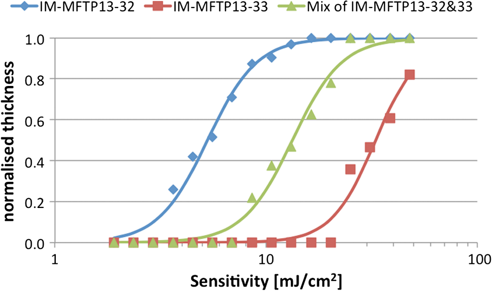
We observed that adopting thinner films seemed to introduce further roughening in the line edge, as would be anticipated from previous results.19,20 Figure 3 shows two resist films patterned at 30-nm half-pitch. Figure 3(a) shows variant IM-MFPT12-19, spin coated from a propylene glycol methyl ether (PGME) solution at 1000 rpm to give a film thickness of 20 nm, given a postapplication bake of 75°C for 5 min, exposed to EUV at , given a postexposure bake of 90°C for 3 min and developed in MCB:IPA []. Figure 3(b) shows a very similar variant, IM-MFPT12-8, which is known to be marginally less sensitive to EUV than IM-MFPT12-19. In this case, the film concentration was to give a film thickness of 40 nm, and the exposure dose was , but conditions were otherwise the same. It can be seen that the LER is substantially higher in Fig. 3(a) than in Fig. 3(b). Therefore, increasing the resist thickness through improvement in the mechanical stability of the resist or pattern collapse mitigation should lead to improvement in LER at lower half-pitches. The CD versus dose and LER versus dose behavior for a film of variant IM-MTFP12-21, exposed under the same conditions as IM-MFTP12-19 above are shown in Fig. 4(a) and 4(b), respectively. It can be seen that the LER is not significantly increased as the dose goes from 20 to . Fig. 4(a) CD versus dose at two half-pitches, and (b) LER versus dose, for the IM-MFTP12-21 variant. 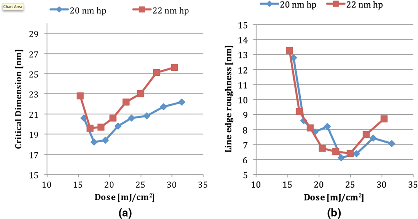 Sensitivity curves for two of the resist variants were also obtained by using an open frame with a square aperture rather than the metal gratings for exposure. From the curves shown in Fig. 5, it can be seen that depending on the synthesis conditions, the material shows a range of variation in sensitivity. Also illustrated is the effect on sensitivity when the two resist materials are used in combination by mixing them together. By adding together the low and high sensitivity materials, a resist with intermediate sensitivity is created. Different developers were tested, as our traditional developer MCB is not acceptable in industrial usage. The exposed material was found to develop as well in 2-heptanone, or in cyclohexanone, two known negative tone developers. A comparison of the developers is shown in Fig. 6 and the resist data are summarized in Table 2. From the table, it can be seen that the 2-heptanone produces smoother lines with a smaller LER but at the cost of a decreased sensitivity. Cyclohexanone shows the reverse characteristics with increased sensitivity at the expense of LER. This seems to suggest that 2-heptanone is a less aggressive developer with reduced solubility of the exposed resist material. The MCB lies on the middle ground in terms of resist performance with both sensitivity and LER lying in the range between the other two chemicals. Fig. 6Comparison of developers for a 22-nm hp pattern: (a) monochlorobenzene:isopropyl alcohol (MCB:IPA), (b) 2-heptanone and (c) cyclohexanone. 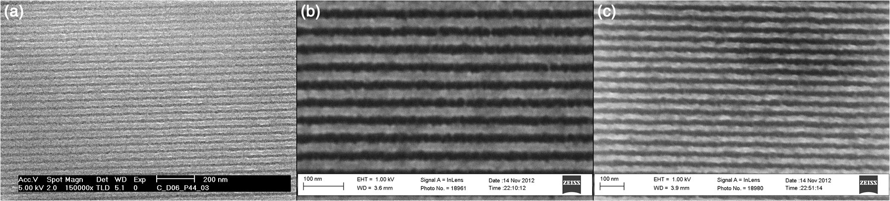 Table 2Resist metrics for different developers.
4.ConclusionWe have presented first results of the EUV exposure of a novel negative tone chemically amplified molecular fullerene resist. The use of fullerenes as resist material is attractive as they have a small molecule size that potentially helps to reduce LER. Furthermore, they have been shown to have a high etch resistance in plasma etching,21 an important factor as progress in lithography has made it necessary to reduce resist thickness. While it was initially surprising to see a tBOC protected phenol used in combination with an epoxy as a good negative tone resist, we have confirmed a significantly better performance than for the unprotected phenol variant of the phenolic fullerene. If the crosslinking component is removed, the negative tone behavior of the tBOC protected phenol is no longer observed, indicating that this is not a simple polarity switch. The mechanism of action is currently being elucidated using a model resist, but we speculate that the acid labile tBOC group is removed by the PAG-generated acid, with the epoxy reaction cationically catalyzed. Analysis of the lithographic performance of the fullerene resist has shown that it possesses resolution, and sensitivity within or close to the target values of the International Technology Roadmap for Semiconductors22 for 2016, but further work is ongoing to reduce LER in the thin films required for high resolution. AcknowledgmentsThe authors thank the Engineering and Physical Sciences Research Council (EPSRC) for support of this project. The Disco DAD 321 wafer dicer used in this research was obtained through Birmingham Science City: Creating and Characterising Next Generation Advanced Materials, with support from Advantage West Midlands (AWM) and partly funded by the European Regional Development Fund (ERDF). The authors would like to thank M. Vockenhuber from PSI for her assistance with the EUV exposures. Part of this work was performed at Swiss Light Source (SLS), Paul Scherrer Institute, 5232 Villigen PSI, Switzerland. ReferencesR. L. Brainardet al.,
“Resists for next generation lithography,”
Microelectron. Eng., 61–62 707
–715
(2002). http://dx.doi.org/10.1016/S0167-9317(02)00564-6 MIENEF 0167-9317 Google Scholar
F. P. Gibbonset al.,
“Fullerene resist materials for the 32 nm node and beyond,”
Adv. Funct. Mater., 18
(13), 1977
–1982
(2008). http://dx.doi.org/10.1002/adfm.v18:13 AFMDC6 1616-3028 Google Scholar
J. Manyamet al.,
“Chemically amplified fullerene resists for e-beam lithography,”
Proc. SPIE, 6923 69230M
(2008). http://dx.doi.org/10.1117/12.772645 PSISDG 0277-786X Google Scholar
H. M. Zaidet al.,
“Chemical amplification of a triphenylene molecular electron beam resist,”
Adv. Funct. Mater., 17
(14), 2522
–2527
(2007). http://dx.doi.org/10.1002/(ISSN)1616-3028 AFMDC6 1616-3028 Google Scholar
T. Tadaet al.,
“A triphenylene derivative as a novel negative/positive tone resist of 10 nanometer resolution,”
Microelectron. Eng., 53
(1–5), 425
–428
(2000). http://dx.doi.org/10.1016/S0167-9317(00)00348-8 MIENEF 0167-9317 Google Scholar
R. A. LawsonL. M. TolbertC. L. Henderson,
“Single component molecular resists containing bound photoacid generator functionality,”
Proc. SPIE, 7273 72733C
(2009). http://dx.doi.org/10.1117/12.814426 PSISDG 0277-786X Google Scholar
W. A. C. Baueret al.,
“Combinatorial optimization of a molecular glass photoresist system for electron beam lithography,”
Adv. Mater., 23
(45), 5404
–5408
(2011). http://dx.doi.org/10.1002/adma.201103107 ADVMEW 0935-9648 Google Scholar
M. Trikeriotiset al.,
“A new inorganic EUV resist with high-etch resistance,”
Proc. SPIE, 8322 83220U
(2012). http://dx.doi.org/10.1117/12.916384 PSISDG 0277-786X Google Scholar
J. K. Stowerset al.,
“Directly patterned inorganic hardmask for EUV lithography,”
Proc. SPIE, 7969 796915
(2011). http://dx.doi.org/10.1117/12.879542 PSISDG 0277-786X Google Scholar
J. Manyamet al.,
“Low activation energy fullerene molecular resist,”
Proc. SPIE, 7273 72733D
(2009). http://dx.doi.org/10.1117/12.814088 PSISDG 0277-786X Google Scholar
J. Manyamet al.,
“Characterization of the effects of base additives on a fullerene chemically amplified resist,”
Proc. SPIE, 7639 76391N
(2010). http://dx.doi.org/10.1117/12.846581 PSISDG 0277-786X Google Scholar
J. Manyamet al.,
“Positive tone chemically amplified fullerene resist,”
Proc. SPIE, 8325 83251U
(2012). http://dx.doi.org/10.1117/12.916472 PSISDG 0277-786X Google Scholar
A. Frommholdet al.,
“Chemically amplified fullerene resists, spin-on fullerene hardmasks and high aspect ratio etching,”
in 12th IEEE Conf. Nanotechnology (IEEE-NANO),
(2012). Google Scholar
C. Bingel,
“Cyclopropanation of fullerenes,”
Chem. Ber., 126
(8), 1957
–1959
(1993). http://dx.doi.org/10.1002/(ISSN)1099-0682 CHBEAM 0009-2940 Google Scholar
X. CampsA. Hirsch,
“Efficient cyclopropanation of C60 starting from malonates,”
J. Chem. Soc. Perkin Trans., 1 1595
–1596
(1997). http://dx.doi.org/10.1039/A702055D Google Scholar
A. Frommholdet al.,
“High aspect ratio etching using a fullerene derivative spin-on-carbon hardmask,”
Proc. SPIE, 8328 83280U
(2012). http://dx.doi.org/10.1117/12.916426 PSISDG 0277-786X Google Scholar
B. Päivänrantaet al.,
“Sub-10 nm patterning using EUV interference lithography,”
Nanotechnology, 22
(37), 375302
(2011). http://dx.doi.org/10.1088/0957-4484/22/37/375302 NNOTER 0957-4484 Google Scholar
A. Frommholdet al.,
“Fullerene-based spin-on-carbon hardmask,”
Microelectron. Eng., 98 552
–555
(2012). http://dx.doi.org/10.1016/j.mee.2012.07.019 MIENEF 0167-9317 Google Scholar
Y. Ekinciet al.,
“Evaluation of resist performance with EUV interference lithography for sub-22 nm patterning,”
Proc. SPIE, 8322 83220W
(2012). http://dx.doi.org/10.1117/12.916541 PSISDG 0277-786X Google Scholar
B. Cardineauet al.,
“LER limitations of resist thin films,”
J. Photopolym. Sci. Technol., 25
(5), 633
–640
(2012). http://dx.doi.org/10.2494/photopolymer.25.633 JSTEEW 0914-9244 Google Scholar
J. Manyamet al.,
“Plasma etching of high-resolution features in a fullerene molecular resist,”
Proc. SPIE, 7972 79722N
(2011). http://dx.doi.org/10.1117/12.879469 PSISDG 0277-786X Google Scholar
International Technology Roadmap for Semiconductors
(2013) http://www.itrs.net/Links/2012ITRS/Home2012.htm 6 ). 2013). Google Scholar
Biography Andreas Frommhold graduated from the Ilmenau University of Technology with a Dipl. Ing. degree in electrical engineering in 2000. He obtained his PhD in electrical engineering in 2010 for work on nanostructure modification of neural implants at the University of Birmingham. He is currently a research fellow in the School of Chemical Engineering at the University of Birmingham. His research interests include chemically amplified molecular resists for electron beam and EUV lithography, as well as the development of nanomaterials for micro- and nanofabrication and plasma etching.  Dongxu Yang obtained his bachelor’s degree (2011) at Sichuan University (China), majoring in applied physics. He is currently undertaking doctoral study at the University of Birmingham (UK). His research has been focused on novel molecular resists for electron beam and extreme ultraviolet lithography.  Alexandra McClelland has been the general manager of Irresistible Materials since September 2011. As well as carrying out research into resist materials for commercial exploitation, she is responsible for driving technical development of resist technology. Previously, she was the lead scientist on a number of research programs for QinetiQ, the defense research company. Her core expertise is in the field of microelectromechanical (MEMS) sensor components such as magnetometers and accelerometers and in the realization of novel resonant MEMS structures. She spent significant time developing etching processes using statistical methodologies such as response surface methodology, specifically using deep dry etching. She subsequently expanded her expertise into novel device design and testing and became the technical lead and focus for several activities.  Xiang Xue Joined Nano-C in 2008, after receiving his PhD in organic chemistry from Boston College, where his work focused on polycyclic aromatic hydrocarbon synthesis and the mechanism of thermal cyclodehydrogenations. He has worked on organic, inorganic and polymer material syntheses for 12 years. He obtained his BS and MS in chemistry at Nanjing University, China. At Nano-C, his research is primarily focused on the preparation and functionalization of fullerenes and carbon nanotubes, and their applications. He has published 10 papers and has several patents pending.  Yasin Ekinci received his PhD from Max Planch Institute for Dynamics and Self Organization in Göttingen, Germany, in 2003. He worked as a postdoc at Paul Scherrer Institute, after which he was a lecturer at ETH Zurich. Since 2009, he has been a senior scientist at Paul Scherrer Institute. He is the manager of the XIL-II beamline at Swiss Light Source. He leads the nano-optics group in Laboratory for Micro- and Nanotechnology where he works on EUV interference lithography and nanooptics.  Richard E. Palmer is professor of experimental physics at the University of Birmingham and head of the Nanoscale Physics Research Laboratory. His research interests include atomic clusters, biochips, atomic manipulation, and nanofabrication. He obtained his first degree (1983) and PhD (1986) at Cambridge University, where he held 1851, Clare College, and Royal Society Research Fellowships. He has held visiting positions at Cornell, Oxford, andHarvard Universities and the Technical University of Denmark. He has been elected to honorary professorships at the University of Wales, Swansea, Harbin Institute of Technology, China, and the Petronas University of Technology, Malaysia. He was awarded an honorary doctoral degree (dr. h.c.) by Hasselt University, Belgium, in 2010 “for his pioneering work in nanoscale physics and his contributions to bridging the gap between nanoscience and nanotechnology.” In 2012, he was elected fellow of the Royal Society of Chemistry and won a senior EPSRC Fellowship.  Alex P. G. Robinson is a senior research fellow of the Science City Research Alliance at the Universities of Birmingham and Warwick. He obtained his PhD in 2000, for work on molecular resist materials done in the Nanoscale Physics Research Laboratory at University of Birmingham and the Joint Research Center for Atom Technology in Japan. His research interests have included modification of oxide surfaces using self assembled mono- and multilayers, coaxial field emission tips, nanostructured biosensors and bio interface surfaces, and resist properties of amorphous low molecular weight materials, low energy electron beam resists, chemically amplified molecular resists for electron beam and EUV lithography, and ICP etching. He is a chartered physicist, fellow of the Higher Education Academy, member of the Institute of Physics and member of SPIE. |