|
|
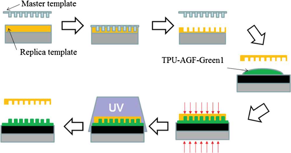
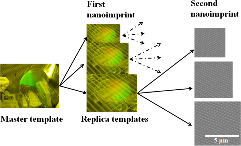
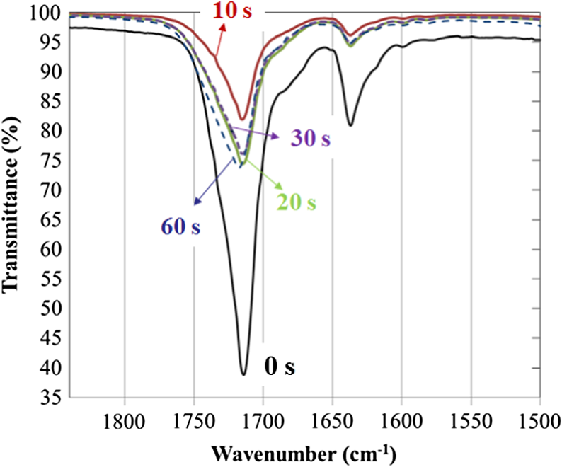
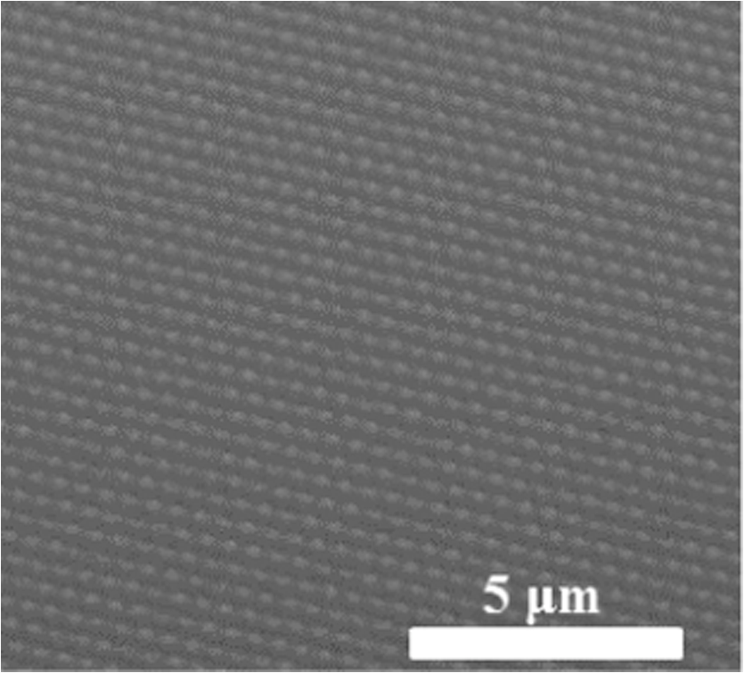
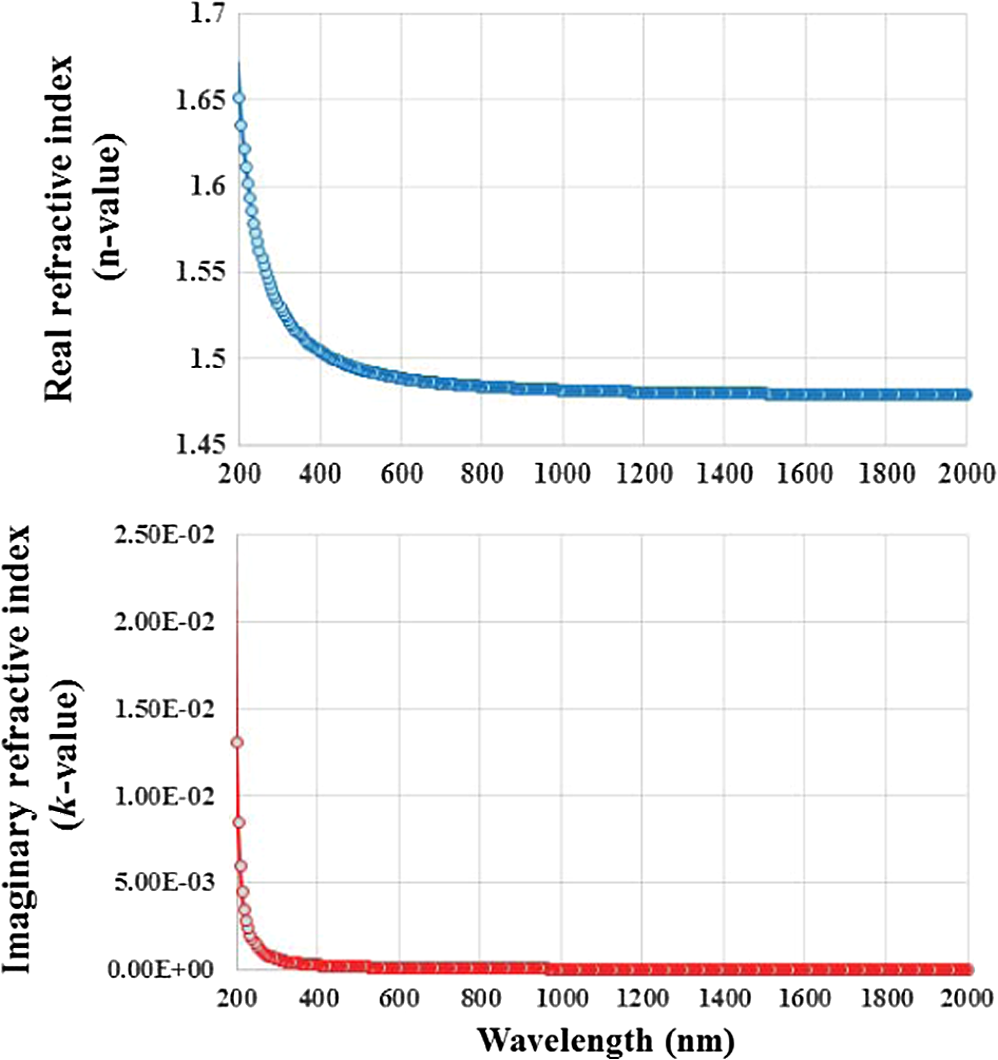
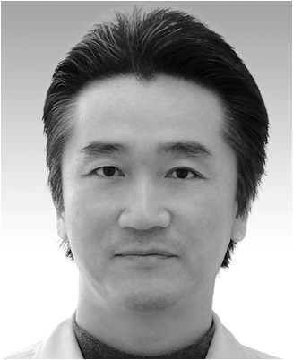
1.IntroductionOptical films such as antireflection film and antiglare film are used in liquid crystal display and electroluminescence display. The films remove glare from glass and plastic while enhancing richer colors, deeper blacks and maintaining sharper images and uniformity. As the pixel size of a display unit become smaller, the influence of display image qualities on reflection of surrounding scenery is critical. An antiglare film with the optical performance, such as high transparency and suitable refraction index in high-definition display, which has a small pixel size, is one of the keys to improving the reflection of the surrounding scenery in a high-definition display surface. A traditional antiglare film is created from a blend of nanoparticles in a polymer matrix or some blended polymers with different refractive indices. The antireflection coating layer of ZnO film was reported on glass.1 Anodic porous alumina nanostructures have been fabricated with tapered and cylindrical pores for a biomimetic antireflecting surface.2 3-(Trimethoxysilyl) propyl methacrylate and fluoroalkylsilane modified silica particles were developed for antiglare film.3 The effects of the solvents in coatings and process temperature on the haze of antiglare films were evaluated.4 Antiglare films with various inner haze and outer haze were fabricated by using light-scattering particles.5 As an alternative to photolithography processes to obtain various nanostructures, ultraviolet curing nanoimprint lithography has been proposed and pursued in creating nanostructures.6–11 Ultraviolet curing nanoimprint lithography has existed for several years and has demonstrated great potential for advanced electronic nanofabrication endeavors in the industrial production of many semiconductors, hard disk drive storage devices, light-emitting diodes, solar cell devices, actuators, biosensors, and microelectro mechanical systems. Ultraviolet curing nanoimprint lithography to yield optical structures is being pursued in optics and photonics to yield low-cost optical components. This is one of the several emerging lithography technologies for low-cost and high-throughput fabrication of polymer optical films. Nanoimprint lithography reduces costs by eliminating the expensive radiation sources and precision optics needed for photolithographic systems. The methodology used in our previous studies is useful in evaluating the work described in this article. In our previous studies,12–15 a series of lactulose, glucose, trehalose, dextrin, and cyclodextrin derivertives in resist materials and the underlayer derived from biomass were developed as candidate materials for advanced photolithography and nanoimprint lithography. These raw materials are a good source of energy and carbon instead of oil resources and are present in a wide variety of sugar-related organic compounds including plants, bacteria, yeast, fungi, insects, and invertebrates. These sugar-related organic compounds are soluble in a variety of organic solvents and are suitable for high refractive index and diffraction gratings with subwavelength structures in optical applications due to rigid ring structures of glucose units and their excellent optical clarity at wavelengths from 250 to 2000 nm. In general, these materials have a chemical structure with results in a refractive index of 1.45 to 1.55 for wavelengths between 250 and 2000 nm. Most antiglare films are optical polymers derived from oil. However, little is known about ecofriendly antiglare films derived from biomass using ultraviolet curing nanoimprint lithography. The solutions of antiglare films are expected to be easily formed into nanostructured materials by nanoimprint lithography processes such as molding, casting, stamping, embossing, etc., which lead to rapid low-cost shaping for advanced high-definition liquid crystal displays and electroluminescence displays with high transparency and a suitable index of refraction. This article presents the progress in developing the new ecofriendly nanoparticles-free antiglare film of sugar-related organic compounds derived from biomass and evaluates the transparency, refractive index, nanopatterning properties, and volumetric shrinkage of antiglare film in the cross-linking process of ultraviolet curing nanoimprint lithography. 2.Experimental Procedure2.1.Preparation of Sugar-Related Organic CompoundsTwo specific glucose and trehalose derivatives with ultraviolet curable acryloyl groups were synthesized as sugar-related organic compounds derived from biomass for minimizing volumetric shrinkage of resist film during ultraviolet polymerization and obtaining a suitable refractive index. The chemical structures of sugar-related organic compounds in antiglare film derived from biomass are shown in Fig. 1. These glucose and trehalose derivatives have five to seven ultraviolet curable acryloyl groups instead of hydroxyl group of glucose and trehalose. The resulting sugar-related organic compounds were subjected to a gel permeation chromatography system (GPC; HLC-8320GPC EcoSEC, Tosoh). GPC uses two separation columns of SuperAW3000 and SuperAW-H (TSK-GEL, Tosoh) and , -dimethylformamide. A column temperature was maintained at 40°C, and the solvent flow rate was set at . The weight average molecular weights of glucose and trehalose derivatives were 700 and 1200, respectively, in terms of the standard polystyrene. Fig. 1Chemical structures of (a) trehalose derivatives and (b) glucose derivatives, (c) isobornyl methacrylate, and (d) 2-methyl-1-phenyl-propan-2-ol in ecofriendly antiglare film derived from biomass.  Isobornyl methacrylate, 2-methyl-1-phenyl-propan-2-ol, and synthetic additives were blended with these specific glucose and trehalose derivatives. Isobornyl methacrylate was used as a diluent for improving the coating properties and 2-methyl-1-phenyl-propan-2-ol was also used as a liquid radical initiator for ultraviolet curing reaction. The developed material of antiglare film was named TPU-AGF-Green1. The specific glucose and trehalose derivatives with photocurable acryloyl groups in TPU-AGF-Green1 are liquids at room temperature, nonsolvent system, low viscosity, and low surface free energy for ultraviolet curing nanoimprint lithography. The low viscosity of antiglare material using ultraviolet curing nanoimprint lithography can be expected to fill the topography of template (mold) in the condition of low imprint pressure. The viscosity was measured by a rheometer (Visco Analyzer VAR100, Reorojika). The viscosity of TPU-AGF-Green1 was 30 cP at 25°C, which makes the material suitable for ultraviolet curing nanoimprint lithography system. In addition, the surface free energy of nanoimprint material plays a key role in the smooth filling of the relief images in the imprint template prior to the ultraviolet curing process. The contact angles of water, -hexadecane, and diiodomethane on TPU-AGF-Green1 layer were measured using a dynamic contact angle analyzer (DropMaster500Z, Kyowa Interface Science) as follows (analysis method: method, drop amount: 1.0 μl, measurement time after droping: 1.0 s). The surface free energy of TPU-AGF-Green1 was calculated using the reported surface free energy components of water, -hexadecane, and diiodomethane, together with the experimental contact angles of water, -hexadecane, and diiodomethane on TPU-AGF-Green1 layer in Owens who extended the Fowkes concept.16–18 The surface free energy of TPU-AGF-Green1 was . The structure of sugar-related organic compounds derived from biomass contributes to lowering the viscosity, while the photocurable acryloyl groups in TPU-AGF-Green1 provide an acceptable surface free energy in the fundamental evaluation of eco-friendly antiglare film with liquid glucose and trehalose derivatives. Two specific glucose and trehalose derivatives with distinctive bulky structures were expected to decrease the film thickness shrinkage during ultraviolet irradiation process of nanoimprinting. In order to adjust the ultraviolet curing time to during ultraviolet irradiation, the concentrations of acryloyl groups were controlled in TPU-AGF-Green1. The design concepts of antiglare film using the sugar-related organic compounds derived from biomass are first demonstrated for next generation optical devices using ultraviolet curing nanoimprint lithography. 2.2.Double Ultraviolet Curing Nanoimprint Lithography Using Disposable Replica TemplateIn order to avoid defective issues on the master template and create a manufacturable process, a double ultraviolet curing nanoimprint lithography was used to make a disposable replica template. This process was then applied to evaluate both size and pitch uniformity of pillar patterns. Ultraviolet curing nanoimprint lithography requires repetitious mechanical contact between a template and the resist material to replicate the template patterns. Figure 2 shows the flowchart of double ultraviolet curing nanoimprint lithography using the disposable replica template from a polyolefin-based master template with pillar patterns of 230-nm diameter and 200-nm height. The diameter of the circle polyolefin-based master template was 10 mm. The polyolefin-based sheet was purchased as a master template from SCIVAX. -based materials of replica template were dropped on to the glass sheet. Silicone elastomer and curing agent Sylgard 184 (Dow Corning) were prepared as -based material for the replica template. The -based material of replica template was blended and dispensed on a glass sheet after deforming at 50°C for 12 h. The master template was then brought into contact with -based materials of replica template, such that the recesses in the glass sheet were filled through capillary force at room temperature for 30 min. Once -based materials of replica template had completely filled the features on the master template, thermal curing was maintained at 40°C for 1 to 2 h using thermal nanoimprint lithography. The master template was then removed from the replica template. The resist material TPU-AGF-Green1 was dispensed onto the underlayer, and TPU-NIL-U01 was used as the adhesion layer.19,20 TPU-NIL-U01 was manually dispensed and spun to the appropriate thickness based on the dry etching processes and then polymerized at 200°C for 60 s. TPU-AGF-Green1 was pressed with the replica template and was filled at room temperature for 120 s. The imprint force was 60 N. TPU-AGF-Green1 was then irradiated by brief ultraviolet irradiation, forming the desired pattern with pillar patterns of 230-nm diameter and 200-nm height. Ultraviolet irradiation was carried out by using a metal halide lamp system (Sun Energy, broad band targeted for the 365-nm peak, ultraviolet exposure dose: for 5 min). Ultraviolet irradiation of TPU-AGF-Green1 with ultraviolet curable acryloyl groups through the quartz plate leads to the radical polymerization in the imprinted area. The replica template is then removed leaving the inverted three dimensional replica of the pattern formed in the polymerized resist material. This process was repeated across the wafer, similar to the double nanoimprint lithography using replica template from a master template. The pattern profiles were observed by scanning probe microscopy (SPM; Shimadzu SPM-9700). Figure 3 shows replication of several imprint process cycles. This technology enables the fabrication of three-dimensional (3-D) patterns and very small structures that have features on the order of 200 nm or smaller.21–27 Nanofabrication provides greater process control while allowing continued reduction of the minimum feature dimensions of the structures formed. In ultraviolet curing nanoimprint lithography, low volumetric shrinkage of the material during ultraviolet irradiation strongly influences nanopattern profiles and high-processing accuracy. 2.3.Ultraviolet Curing Properties of Antiglare Film TPU-AGF-Green1 Derived from BiomassNanoimprint lithography must deal with concerns over generated defects due to the repetitious mechanical contact between the template and a nanoimprint material. The progress of the ultraviolet cross-linking reaction and ultraviolet curing properties of antiglare film TPU-AGF-Green1 derived from biomass were evaluated in Fig. 4, in order to induce the anti-adhesion of TPU-AGF-Green1 to the template. Fig. 4Ultraviolet curing properties by (a) Fourier transform infrared spectroscopy and (b) solvent stripping processes. 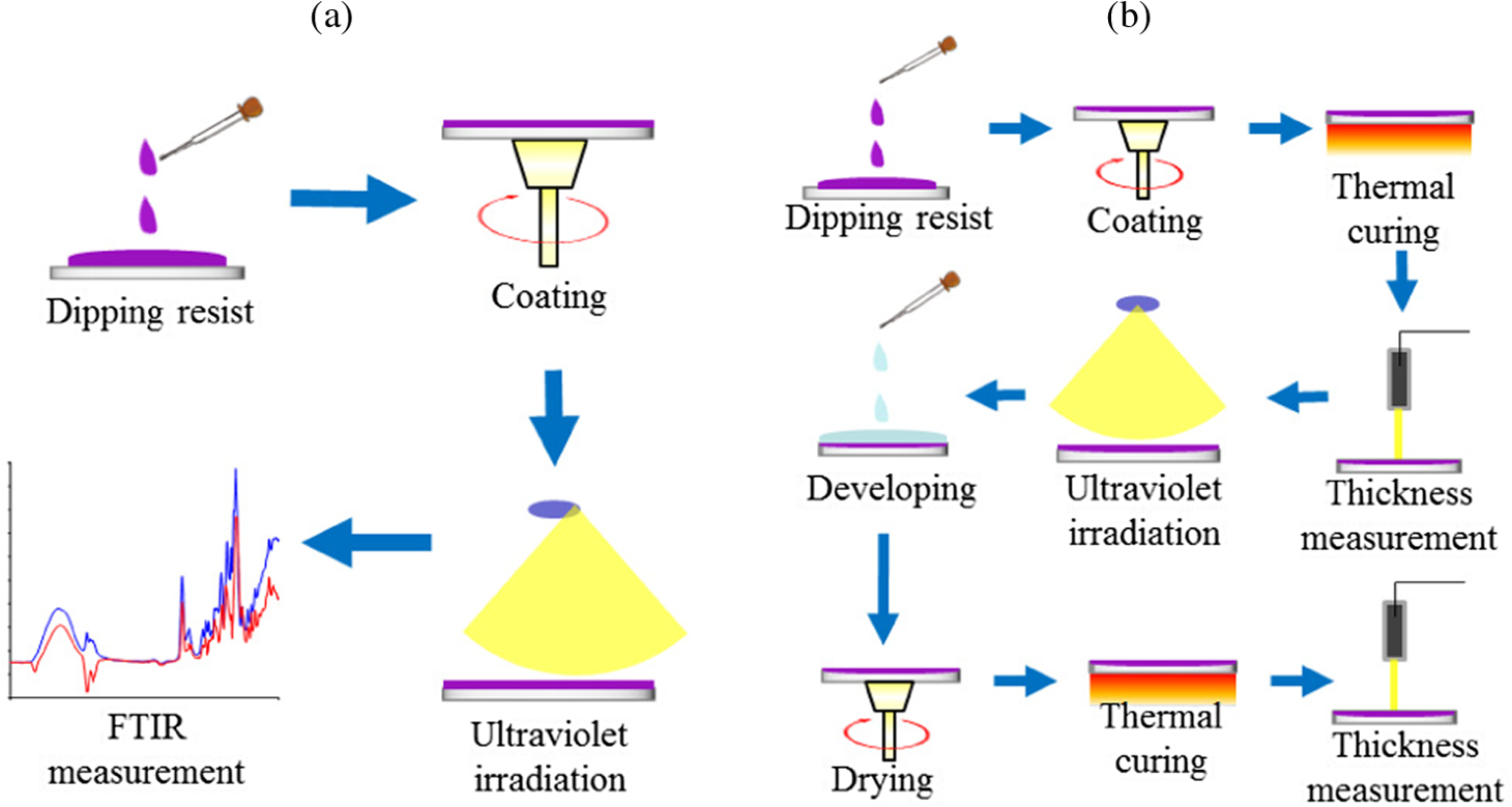 FTIR also has efficacy as bonding configuration analysis of ultraviolet curable acryloyl groups during the ultraviolet irradiation. The peak at around corresponding to stretching vibration of ultraviolet curable acryloyl groups in sugar-related organic compounds such as glucose derivatives, trehalose derivatives, and isobornyl methacrylate as a diluent for improving the coating properties was measured using ATR-FTIR spectroscopy SpectrumTwo (PerkinElmer, Kanagawa, Japan). The peak at around was also measured to the stretching vibration of carbonyl groups in 2-methyl-1-phenyl-propan-2-ol as a liquid radical initiator for ultraviolet curing reaction. In addition to the above change of concentration of ultraviolet curable acryloyl groups in TPU-AGF-Green1, a stripping test was performed to determine the resistance of TPU-AGF-Green1 to the solvents, in order to obtain anti-adhesion information of the nanoimprint material to the replica template. The solutions of the above solvent diluted nanoimprint material of TPU-AGF-Green1 were spun onto the prepared under layer TPU-NIL-U01 at 1500 rpm for 60 s and then polymerized in ultraviolet polymerization at for 5 min. The thickness of TPU-AGF-Green1 on TPU-NIL-U01 was then measured using a thin film measurement system F20-UV (Filmetrics, Kanagawa, Japan). The thickness of TPU-AGF-Green1 was . The wavelength range of 300 to 700 nm and the reflectance from the top and bottom of the layer were used. Ethyl lactate, cyclohexanone, propylene glycol monomethyl ether, and propylene glycol monomethyl ether acetate were dispensed on the coated film of TPU-AGF-Green1. After 2 min, TPU-AGF-Green1 was spin dried at 1500 rpm for 1 min and at 5000 rpm for 2 min. The thickness of TPU-AGF-Green1 was then measured again. The amount of stripping was determined to be the difference between the initial and final thicknesses of TPU-AGF-Green1. 2.4.Volumetric Shrinkage of TPU-AGF-Green1 Derived from Biomass During Ultraviolet IrradiationIn order to obtain higher processing accuracy of ultraviolet curing nanoimprint lithography, low volumetric shrinkage of material as one of key factors was evaluated in ultraviolet curing reactions of radical and polymerization using ultraviolet curable acryloyl groups. Low volumetric shrinkage of material during ultraviolet irradiation influences nanopattern profiles and high-processing accuracy. In order to evaluate the amount of volumetric shrinkage of TPU-AGF-Green1, the difference between the initial and final thicknesses was measured in the following ultraviolet irradiation process. The film thickness shrinkage of the ultraviolet irradiation process was calculated from the difference of film thickness on substrates by a use of the thin film measurement system before and after the ultraviolet irradiation. The solutions of the solvent diluted nanoimprint material of TPU-AGF-Green1 were spun onto a 100-mm silicon wafer for 60 s and then polymerized in ultraviolet polymerization at for 5 min. The thickness of TPU-AGF-Green1 was . Ultraviolet irradiation was carried out by using the above metal halide lamp system (broad band targeted for the 365-nm peak, ultraviolet exposure dose: ). The thicknesses of TPU-AGF-Green1 were again measured after the ultraviolet irradiation process. The amount of film thickness shrinkage of ultraviolet irradiation process of TPU-AGF-Green1 was calculated to be the difference between the initial and final thicknesses. To compare the film thickness shrinkage of materials, a referenced nanoimprint material consisting of isobornyl acrylate (50 wt%) as the etch resist, ethylene glycol diacrylate (20 wt%) as the crosslinker, -butyl acrylate (27 wt%) as the diluent, and 2-hydroxy-2-methyl-1-phenyl-1-propanone (3 wt%) as the photoinitiator was prepared as the first reference. This referenced material with acrylate group for radical polymerization was named as Ref-Acrylate, and a commercially available resist material chosen as the second reference was mr-UVCur06 (Micro Resist Technology, Berlin, Germany) with unknown ultraviolet reactive groups for polymerization. 2.5.Optical Transparency and Refraction Index of TPU-AGF-Green1 Derived from BiomassProperties of an antiglare film include a high transparency of and a refraction index between 1.45 and 1.53 for wavelengths ranging from 350 to 800 nm. The real refractive index (-value) and imaginary refractive index (-value) of TPU-AGF-Green1 were measured using a GES5E ellipsometer (SOPRALAB, Kanagawa, Japan). The solutions of the above solvent diluted nanoimprint material of TPU-AGF-Green1 were spun onto a 200-mm silicon wafer at 3000 rpm for 60 s and then polymerized in ultraviolet polymerization at for 5 min. The thickness of TPU-AGF-Green1 was . TPU-AGF-Green1 was evaluated to be applicable to future development of antireflective material with subwavelength structures and suitable refractive index material as a chemical design of sugar-related organic compounds derived from biomass. 2.6.Gas Barrier Properties of TPU-AGF-Green1 Derived from Biomassgas barrier properties in TPU-AGF-Green1 and a referenced polyethylene with a weight average molecular weight of 15,000 and a polydispersity of 2.7 were measured by gas barrier testing system GTR (GTR Tec, Kyoto, Japan). TPU-AGF-Green1 and the referenced polyethylene were casted on a stainless mesh and baked on a hotplate at 250°C for 300 s after prebaking at 120°C for 60 s. The thickness of TPU-AGF-Green1 and the referenced polyethylene were . 3.Results and Discussion3.1.Ultraviolet Curing Properties of TPU-AGF-Green1 Derived from BiomassThe separation and release of the template from TPU-AGF-Green1 are crucial to the high-processing accuracy of the lithographic patterns. Figure 5 shows the time-dependent FTIR spectra of TPU-AGF-Green1 in the spectral range from 1500 to . A peak at around corresponding to stretching vibration of ultraviolet curable acryloyl groups and also the peak at around corresponding to the stretching vibration of carbonyl groups was observed in TPU-AGF-Green1. Time-dependent FTIR spectra of TPU-AGF-Green1 indicated an obvious decrease of both stretching vibration of ultraviolet curable acryloyl groups and stretching vibration of carbonyl groups. In addition, stripping tests using cyclohexanone, propylene glycol monomethyl ether, and propylene glycol monomethylether acetate showed no detectable changes in the film thickness () of TPU-AGF-Green1. The developed sugar-related organic compounds derived from biomass of TPU-AGF-Green1 were shown to be polymerized on the basis of its solvent resistance.28,29 It was obvious that eco-friendly antiglare film TPU-AGF-Green1 derived from biomass was polymerized by ultraviolet irradiation, in order to avoid generating the defects when separated TPU-AGF-Green1 from disposable replica template. 3.2.Ultraviolet Curing Nanoimprint Lithography of TPU-AGF-Green1 Derived from BiomassSPM images of master template with pillar patterns of 230-nm diameter and 200-nm height and TPU-AGF-Green1 in the single ultraviolet curing nanoimprint lithography without a disposable replica template are shown in Fig. 6. The reversed pattern of 230-nm diameter in TPU-AGF-Green1 was resolved using the above process conditions. TPU-AGF-Green1 derived from biomass indicated specific desired properties of ultraviolet curing nanoimprint lithography. Figure 7 shows the SPM images of the same master template, the imprinted disposable replica template using the master template, and the imprinted TPU-AGF-Green1 patterning profiles in the double ultraviolet curing nanoimprint lithography using disposable replica template. The great anti-adhesion of TPU-AGF-Green1 and disposable replica template in areas was effective in avoiding the disposable replica template contamination when the disposable replica template was removed from TPU-AGF-Green1 after ultraviolet irradiation. Figure 8 also shows the microscope image of the imprinted TPU-AGF-Green1 patterning profiles in approximately areas. The chemical modification of ultraviolet curing reactions was considered to be effective for obtaining the rounded pattern profiles. The validity of our new approach of material design using the sugar-related organic compounds derived from biomass with ultraviolet curable acryloyl groups was confirmed experimentally for ecofriendly antiglare film. Fig. 6Scanning probe microscopy (SPM) images of master template with pillar patterns of 230 nm diameter and TPU-AGF-Green1 in single ultraviolet curing nanoimprint lithography. 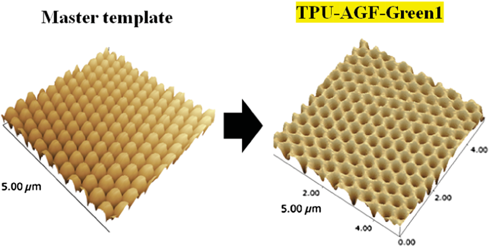 Fig. 7SPM images of master template with pillar patterns of 230 nm diameter, replica templates and TPU-AGF-Green1 in double ultraviolet curing nanoimprint lithography. 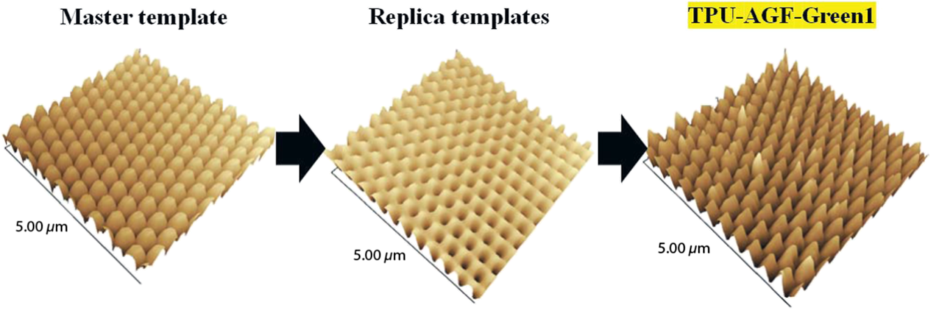 In addition, the size uniformity of diameter and the pitch in pillar patterns after double nanoimprint processes were obtained on five different areas within the 10-mm diameter circle such as the center, upper, left, right, and under of master template and TPU-AGF-Green1 as shown in Fig. 9. According to the measurement result of the diameter and the pitch by calculating the sharpness of SPM images on master template and TPU-AGF-Green1, the size biases of diameter and the pitch between master template and TPU-AGF-Green1 were only 20 nm. The measured result of diameter and the pitch of master template and TPU-AGF-Green1 were considered to be variability of the data by calculating the sharpness of SPM images in five different 5 areas, and the result of diameter and the pitch seem random with central size of 230-nm diameter. We attribute the 20-nm variation in the diameter and the pitch to SPM measurement used for this work. Fig. 9Size uniformities of diameter and the pitch of master template and TPU-Green1 with pillar patterns. 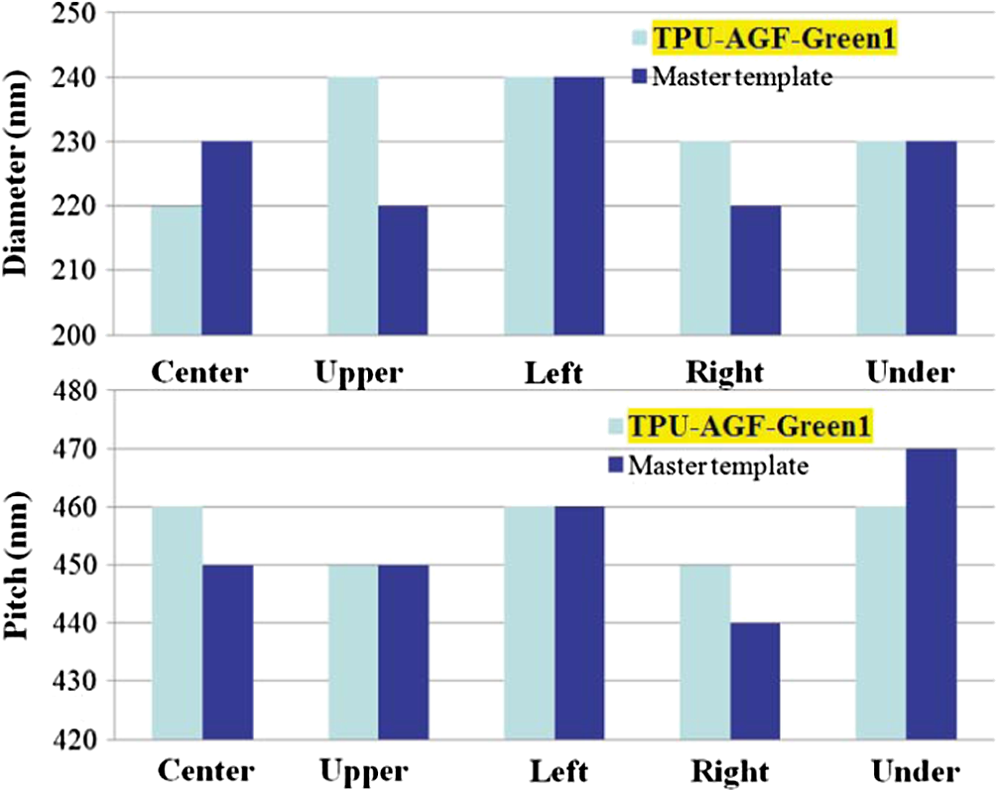 The processing accuracy of TPU-AGF-Green1 was considered to be acceptable to fabricate the basic study for optical materials derived from biomass with subwavelength structures of 350 to 800 nm required in the antiglare film of liquid crystal display and electroluminescence display. The relationship between chemical modification of ultraviolet curing reactions and processing accuracy of height in TPU-AGF-Green1 should be carefully investigated in future studies. 3.3.Volumetric Shrinkage of TPU-AGF-Green1 Derived from Biomass During Ultraviolet IrradiationFilm thickness shrinkage of ultraviolet curing process of TPU-AGF-Green1 was 4.8%. The above referenced acryl-based resist material [isobornyl acrylate (50 wt%), ethylene glycol diacrylate (20 wt%), -butyl acrylate (25 wt%), a photoinitiator, and tridecafluro-1,1,2,2-tetrahydrooctyldimethylchlorosilane (2 wt%)] and mr-UVCur06 had the film thickness shrinkage of ultraviolet curing process of 8.9% and 8.7%, respectively. TPU-AGF-Green1 indicated a lower film thickness shrinkage of ultraviolet curing process than the two referenced resist materials. The starting thicknesses for all the samples tested were . The distinctive bulky glucose structures in sugar-related organic compounds derived from biomass were considered to be effective for minimizing volumetric shrinkage during ultraviolet irradiation. In addition to the demonstration of antiglare film with new chemical structures for environmentally compatible fabrication, low cost, and high manufacturability, the effect of the bulky chemical structure in glucose and trehalose derivatives for minimizing the film shrinkage was investigated to achieve the nanoimprint images of pillar patterns with high-processing accuracy. Oxetane and epoxy polymerization as one of cationic ultraviolet chemical reactions is expected to be of considerable benefit in minimizing volumetric shrinkage during ultraviolet irradiation in the next material design of antiglare film. The approach of adding oxetane or epoxy group as photoreactive side-chain functionality into the distinctive bulky glucose structures in sugar-related organic compounds derived from biomass is considered to be a key in the characterization of advanced nanoimprint materials. 3.4.Optical Transparency and Refraction Index of TPU-AGF-Green1 Derived from BiomassFigure 10 shows the dependence of wavelength on (a) real refractive index and (b) imaginary refractive index (-value) of TPU-AGF-Green1. TPU-AGF-Green1 was indicated to achieve a real refraction index of 1.45 to 1.53 at 350 to 800 nm and an imaginary refractive index of at 350 to 800 nm. Therefore, TPU-AGF-Green1 has suitable optical transparency and refractive index for an antiglare film and is suitable for future development of antireflective material with subwavelength structures and refractive index material of 1.45 to 1.53 at 350 to 800 nm as a chemical design of sugar-related organic compounds derived from biomass. 3.5.Gas Barrier Properties of TPU-AGF-Green1 Derived from Biomassgas barrier properties of TPU-AGF-Green1 and the referenced polyethylene were compared to calculate transmission rate in 10-μm film thickness. It was found that the transmission rate of in TPU-AGF-Green1 was less than that of in the referenced polyethylene. It was confirmed that TPU-AGF-Green1 had great gas barrier properties owing to radical polymerization by ultraviolet curable acryloyl groups in sugar-related organic compounds such as glucose derivatives, trehalose derivatives, and isobornyl methacrylate in the baking. 4.ConclusionWe reported the progress in the formulation of sugar-related organic compounds derived from biomass for antiglare film using ultraviolet curable nanoimprint lithography for liquid crystal display and electroluminescence display. The sugar-related organic compounds derived from biomass have been developed and have a real refraction index of 1.45 to 1.53 at 350 to 800 nm, low imaginary refractive index of , and low volumetric shrinkage of 4.8% during ultraviolet irradiation. The new sugar-related organic compounds with ultraviolet curable acryloyl groups produced high-processing accuracy of nanostructure images with pillar patterns of 230-nm diameter in the conditions of ultraviolet curable nanoimprint lithography. The sugar-related organic compounds indicated one effect of the ring components containing bulky disaccharide for suitable optical properties. Further optimization such as the concentration of ultraviolet curable groups in sugar-related organic compounds is expected to clearly resolve nanopatterning profiles. The proposed sugar-related organic compounds derived from biomass are expected to be effective in promoting the future production of advanced nanoimprint lithography using a source of energy and carbon instead of oil resources. AcknowledgmentsThis work was supported by Grant-in-Aid for Scientific Research No. 25790036. This project was also partially supported by The Asahi Glass Foundation, The Noguchi Institute Foundation, and The First Bank of Toyama Foundation. The author is deeply grateful to Professor C. Grant Willson of the University of the University of Texas at Austin and of the National Nanotechnology Infrastructure Network (NNIN, Texas) for his encouragement. The author would like to thank Toyama New Industry Organization, Toyama Prefectural Plastic Industries Association, and Toyama Monozukuri Research and Development Center. Specific thanks are due to Professor Hiroshi Miyasaka of Osaka University for his support. ReferencesS. Saliaet al.,
“Nanocrystalline ZnO film deposited by ultrasonic spray on textured silicon substrate as an anti-reflection coating layer,”
Phys. B, 407
(1), 2626
–2631
(2012). http://dx.doi.org/10.1016/j.physb.2012.04.009 PHYBE3 0921-4526 Google Scholar
G. Hubbardet al.,
“Angle dependent optical properties of polymer films with a biomimetic anti-reflecting surface replicated from cylindrical and tapered nanoporous alumina,”
Nanotechnology, 23
(15), 155302
(2012). http://dx.doi.org/10.1088/0957-4484/23/15/155302 NNOTER 0957-4484 Google Scholar
C. C. Changet al.,
“Preparation of polymer/silica composite antiglare coatings on poly(ethylene terphathalate) (PET) substrates,”
J. Coat. Technol. Res., 9
(5), 561
–568
(2012). http://dx.doi.org/10.1007/s11998-011-9392-4 JCTRCP 1935-3804 Google Scholar
B. T. LiuY. T. Teng,
“Effects of affinity of solvents on the haze of anti-glare films,”
Adv. Mater. Res., 557–559 1695
–1698
(2012). http://dx.doi.org/10.4028/www.scientific.net/AMR.557-559 ADMRBX 0568-0018 Google Scholar
B. T. LiuY. T. Teng,
“A novel method to control inner and outer haze of an anti-glare film by surface modification of light-scattering particles,”
J. Colloid Interface Sci., 350
(2), 421
–426
(2010). http://dx.doi.org/10.1016/j.jcis.2010.07.014 JCISA5 0021-9797 Google Scholar
M. A. G. Lazoaet al.,
“UV-nanoimprint lithography and large area roll-to-roll texturization with hyperbranched polymer nanocomposites for light-trapping applications,”
Solar Energy Mater. Solar Cells, 103 147
–156
(2012). http://dx.doi.org/10.1016/j.solmat.2012.04.034 SEMCEQ 0927-0248 Google Scholar
Q. Donget al.,
“A polyferroplatinyne precursor for the rapid fabrication of L10-FePt-type bit patterned media by nanoimprint lithography,”
Adv. Mater., 24
(8), 1034
–1040
(2012). http://dx.doi.org/10.1002/adma.v24.8 ADVMEW 0935-9648 Google Scholar
C. WangStephen Y. Chou,
“Integration of metallic nanostructures in fluidic channels for fluorescence and Raman enhancement by nanoimprint lithography and lift-off on compositional resist stack,”
Microelectron. Eng., 98 693
–697
(2012). http://dx.doi.org/10.1016/j.mee.2012.05.051 MIENEF 0167-9317 Google Scholar
S. W. Leeet al.,
“Highly sensitive biosensing using arrays of plasmonic Au nanodisks realized by nanoimprint lithography,”
ACS Nano, 5
(2), 897
–904
(2011). http://dx.doi.org/10.1021/nn102041m 1936-0851 Google Scholar
H. Linet al.,
“A thiol-ene photo-curable hybrid fluorinated resist for the high-performance replica mold of nanoimprint lithography (NIL),”
J. Mater. Chem., 22
(6), 2616
–2623
(2012). http://dx.doi.org/10.1039/c1jm13765d JMACEP 0959-9428 Google Scholar
S. Takei,
“Plant-based resist materials for ultraviolet curing nanoimprint lithography,”
J. Micro/Nanolithogr. MEMS MOEMS, 9
(3), 033006
(2010). http://dx.doi.org/10.1117/1.3475951 JMMMHG 1932-5150 Google Scholar
S. Takei,
“UV nanoimprint lithography of 70 nm half pitch line pattern using plant-based resist material with lactulose derivative derived from biomass and medicinal drugs,”
Micro Nano Lett., 7
(8), 822
–825
(2012). http://dx.doi.org/10.1049/mnl.2012.0346 NLAEBV 2150-5551 Google Scholar
S. Takeiet al.,
“Eco-friendly electron beam lithography using water-developable resist material derived from biomass,”
Appl. Phys. Lett., 101
(3), 033106
(2012). http://dx.doi.org/10.1063/1.4737639 APPLAB 0003-6951 Google Scholar
S. Takeiet al.,
“Electron beam lithography using highly sensitive negative type of plant-based resist material derived from biomass on hardmask layer,”
Appl. Phys. Express, 4
(10), 106502
(2011). http://dx.doi.org/10.1143/APEX.4.106502 1882-0778 Google Scholar
S. Takei,
“Development of ultraviolet crosslinking glucose-based resist materials for advanced electronic device applications using nanoimprint lithography,”
Jpn. J. Appl. Phys., 50
(1), 01BA02
(2011). http://dx.doi.org/10.1143/JJAP.50.01BA02 JJAPA5 0021-4922 Google Scholar
D. K. OwensR. C. Wendt,
“Estimation of the surface free energy of polymers,”
J. Appl. Polym. Sci., 13
(8), 1741
–1747
(1969). http://dx.doi.org/10.1002/app.1969.070130815 JAPNAB 1097-4628 Google Scholar
F. M. Fowkes,
“Additivity of intermolecular forces at interfaces. I. determination of the contribution to surface and interfacial tensions of dispersion forces in various liquids,”
J. Phys. Chem., 67
(12), 2538
–2541
(1963). http://dx.doi.org/10.1021/j100806a008 JPCHAX 0022-3654 Google Scholar
S. TakeiA. Sekiguchi,
“Nanoimprint resist material containing ultraviolet reactive fluorine surfactant for defect reduction in lithographic fabrication,”
Appl. Sci., 2
(1), 24
–34
(2012). http://dx.doi.org/10.3390/app2010024 1454-5101 Google Scholar
S. Takeiet al.,
“Silicon-containing spin-on underlayer material for step and flash nano imprint lithography,”
Jpn. J. Appl. Phys., 49
(7), 075201
(2010). http://dx.doi.org/10.1143/JJAP.49.075201 JJAPA5 0021-4922 Google Scholar
S. Takeiet al.,
“Advanced step and flash nano imprint lithography using ultraviolet sensitive hard mask underlayer material,”
Micro Nano Lett., 5
(2), 117
–120
(2010). http://dx.doi.org/10.1049/mnl.2010.0014 NLAEBV 2150-5551 Google Scholar
C. G. Willson,
“A decade of step and flash imprint lithography,”
J. Photopolym. Sci. Technol., 22
(2), 147
–153
(2009). http://dx.doi.org/10.2494/photopolymer.22.147 JSTEEW 0914-9244 Google Scholar
T. OgawaS. TakeiC. G. Willson,
“Ultraviolet curable branched siloxanes as low-k dielectrics for imprint lithography,”
J. Vac. Sci. Technol. B, 31
(1), 011601
(2013). http://dx.doi.org/10.1116/1.4770051 JVTBD9 0734-211X Google Scholar
K. S. Selinidiset al.,
“Mask replication using jet and flash imprint lithography,”
J. Micro/Nanolithogr. MEMS MOEMS, 10
(4), 043005
(2011). http://dx.doi.org/10.1117/1.3646523 JMMMHG 1932-5150 Google Scholar
G. M. Schmidet al.,
“Implementation of an imprint damascene process for interconnect fabrication,”
J. Vac. Sci. Technol. B, 24
(3), 1283
–1291
(2006). http://dx.doi.org/10.1116/1.2197508 JVTBD9 0734-211X Google Scholar
K. Selenidiset al.,
“High-resolution defect inspection of step-and-flash imprint lithography for 32-nm half-pitch patterning,”
Proc. SPIE, 7271 72711W
(2009). http://dx.doi.org/10.1117/12.815014 PSISDG 0277-786X Google Scholar
I. McMackinet al.,
“High resolution defect inspection of step and flash imprint lithography for 32 nm half-pitch patterning,”
Proc. SPIE, 6921 69211L
(2008). http://dx.doi.org/10.1117/12.773970 PSISDG 0277-786X Google Scholar
M. W. Linet al.,
“Simulation and design of planarizing materials for reverse-tone step and flash imprint lithography,”
J. Micro/Nanolithogr. MEMS MOEMS, 7
(2), 023008
(2008). http://dx.doi.org/10.1117/1.2896047 JMMMHG 1932-5150 Google Scholar
S. Takeiet al.,
“Development of novel UV cross-linkable materials for enhancing planarity in via applications via the correlation of simulated and experimental analyses,”
Proc. SPIE, 7273 72730W
(2009). http://dx.doi.org/10.1117/12.813530 PSISDG 0277-786X Google Scholar
S. Takeiet al.,
“Advanced ultraviolet cross-link process and materials for global planarization,”
J. Micro/Nanolithogr. MEMS MOEMS, 7
(4), 043005
(2008). http://dx.doi.org/10.1117/1.2990739 JMMMHG 1932-5150 Google Scholar
Biography Satoshi Takei is an associate professor of the Electronic Material Laboratory in Toyama Prefectural University, and a visiting academic staff in Osaka University from 2010. His PhD and industrial experience focused on the electronic material design and lithographic process in the electronic device applications. He was a member of the research staff in the electronic research laboratory of Nissan Chemical Industries from 1998 to 2010. In 2001, he was a visiting assignee of SPT-Lithography in IMEC. In 2009, he was a visiting scientist of Prof. C. Grant Willson laboratory in University of Texas at Austin and the National Nanotechnology Infrastructure Network (NNIN, Texas). His current interests are biomedical material science and engineering using lithography.  Gaku Murakami is an engineer at Richell Cso, where he is engaged in the development and manufacture of microfluidic chips made of resin. Having graduated from the Faculty of Engineering at University of Toyama in 1999, he obtained the master’s degree in 2001 at the graduate school of Science and Engineering for Education, University of Toyama. Yuto Mori received the BS degree in mechanical systems engineering from Toyama Prefectural University, Japan in 2013.  Takumi Ichikawa is a master’s degree student in the Graduate School of Engineering, Toyama Prefectural University. His study is a development of multifunctional materials derived from cellulose and biomass. Atsushi Sekiguchi received BS and MS degrees in mechanical systems engineering from Toyama Prefectural University, Japan, in 2011 and 2013, respectively.  Tsutomu Obata is a research engineer in Toyama Industrial Technology Center from 2004. He specializes in SiGe crystal growth, MEMS devices and biochips. He was a member of research engineer in Hokuriku Electric Industry Co. from 1991 to 2000. From 2001 to 2003, he was a domestic research fellow in JST and JSPS.  Yoshiyuki Yokoyama is a researcher in Toyama Industrial Technology Center. He received BS and MS degrees in chemistry from Tohoku University, Japan, in 1996 and 1998, respectively, and a PhD degree in material science from Japan Advanced Institute of Science and Technology, Japan, in 2011. He was a member of the research staff in the Central Research Laboratory at Hitachi Ltd. from 1998 to 2002 and was engaged in R&D on optical lithography. His current interests are R&D of biomaterial polymer, photo and nanoimprint lithography for tissue engineering.  Wataru Mizuno is a researcher in Toyama Industrial Technology Center. His business is molding and green engineering of polymers. |