|
|
1.IntroductionAs the semiconductor technologies develop, circuit elements are becoming smaller and are thus harder to fabricate using conventional photolithography systems. Scientists have been seeking various ways to solve this problem using alternative lithographical methods. Among them, electron beam lithography (EBL) has been considered as a useful candidate for next-generation lithography.1 EBL consists of three parts as shown in Fig. 1: (1) a digital layout image that is stored at the storage system, (2) a data path through which the layout image is transmitted, and (3) an electron beam writer that writes the transmitted layout image on the photoresist using an electron beam. Instead of masking the layout image patterns from the light source, an EBL system writes the layout image digitally pixel-by-pixel using electron beams. EBL systems have a number of advantages over conventional photolithography systems:
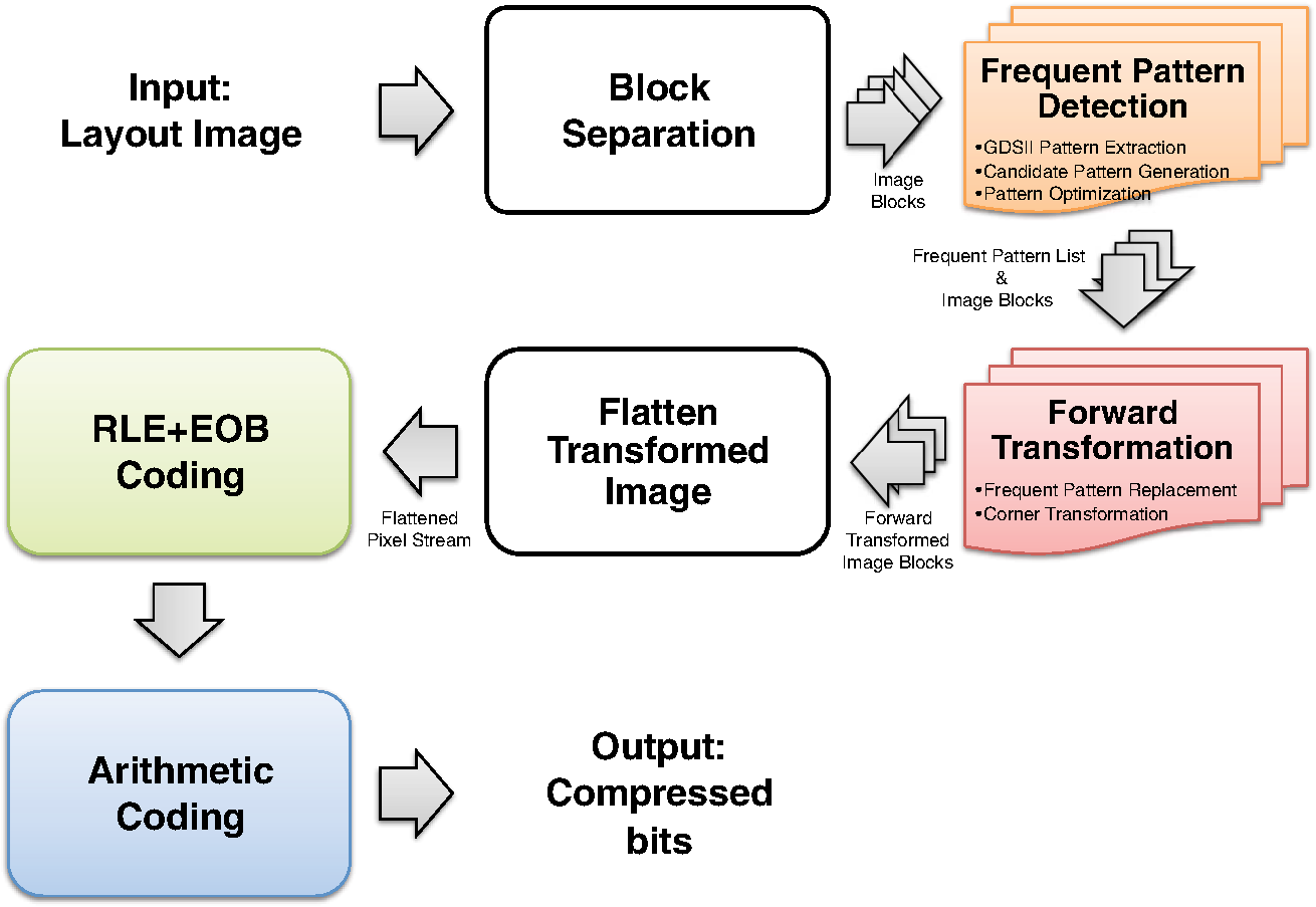
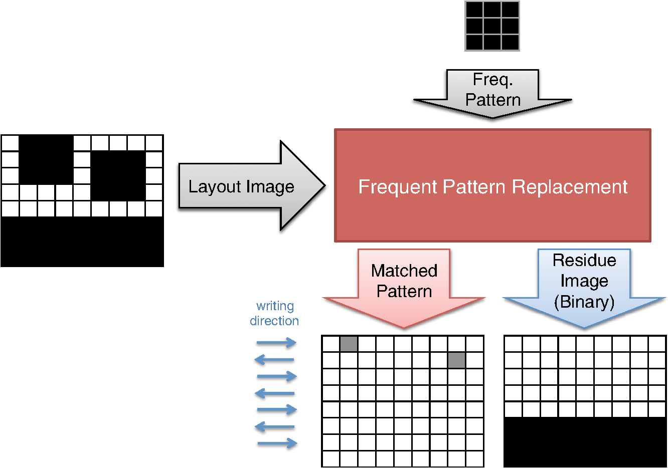
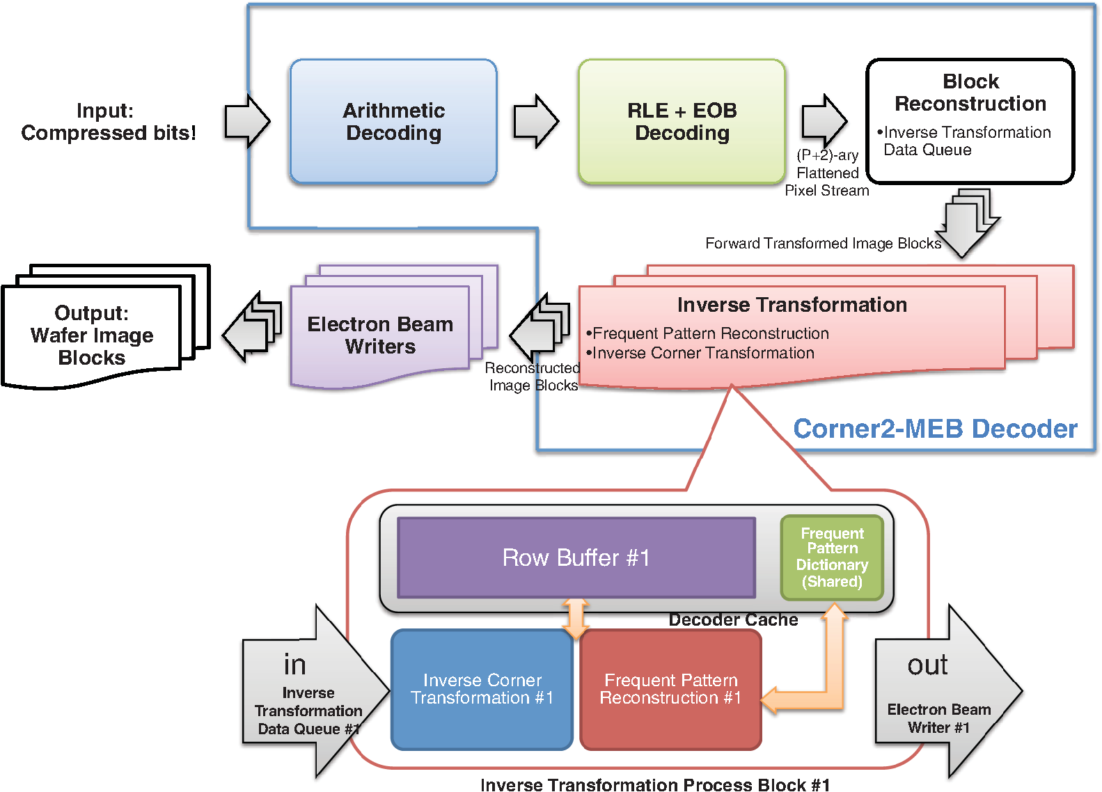
However, EBL systems have a drawback over physical mask lithography systems—they are slow.3 Because EBL systems write layout images pixel by pixel, the throughput of EBL is extremely low and is hence not suitable for the mass production of circuits. Moreover, considering the enormous data requirement—Dai4 suggested 735 Tera pixels are required for a 300-mm wafer using 45-nm technology—to cover the entire wafer, this is unsustainable without massively parallel electron beams. Over the decades, scientists have been trying to solve this problem and are recently attacking it by applying multiple electron beam (MEB) writers to the system.2,4,5,6 By writing multiple pixels at a time, it is possible to decrease the writing time and increase the throughput. Furthermore, by carefully selecting the number of electron beam writers of the EBL systems, it is possible to match the throughput of conventional photolithography systems. Many innovations in MEB lithography are being developed for various applications, such as mask writing, prototyping, writing critical layers in high-volume manufacturing (HVM), and writing all layers in HVM. Recently, Lin1 suggested that MEB direct-write (DW) systems writing all layers in HVM are the most economical option for next-generation lithography technology, especially once the wafer size increases to 450 mm. However, there are still a few outstanding problems to address before MEB DW systems can replace conventional lithography systems, and one of these is the datapath issue. For MEB DW systems to maintain sufficient throughput, many bits must be simultaneously transmitted to the array of electron beam writers. This raises a question of how to provide the massive layout image data (which is typically several hundred terabits per wafer4) to MEB DW systems. Because of a bandwidth shortage between the storage where the layer images are deposited and the MEB DW system, obtaining competitive throughput using an MEB DW system is not possible with conventional datapath methods. Dai and Zakhor3,7 proposed a datapath system with a lossless image compression component. As shown in Fig. 2, they cache compressed layout images in storage disks and send this compressed data to the processor board memory. Then the MEB systems can have higher throughput if the decoder embedded within the array of electron beam writers can quickly recover the original images from the compressed files. Since the decoder cannot store an entire compressed layout image, each compressed layout image is repeatedly transferred from the storage to the decoder as it is written multiple times on a wafer. Cramer et al.8 later improved and tailored the algorithm of Ref. 7 to operate on a particular MEB system called reflective electron beam lithography (REBL).5 Based on the datapath system introduced by Dai and Zakhor,3 Yang and Savari developed a lossless compression algorithm, Corner9 and Corner2,10 that has better compression performance than Block C4 (BC4) (Ref. 7) for both regular and irregular circuits. The Corner2 algorithm utilizes dictionary-based compression to handle repeated circuit components and applies a transform that is specifically tailored for layout images to deal with irregular circuit components. The transformation used in Corner2 utilizes the fact that most polygons in the layout images are Manhattan, i.e., they have right angle corners. This transformation as well as the dictionary-based compression are tailored for the application so that the decoder can reconstruct the layout image with only a small cache requirement. Krecinic et al.11 independently introduced a vertex-based circuit layout image representation format, which can be viewed as a variant of the Corner2 transformation along with a version of run length encoding (RLE) to compress circuit layout images. However, they did not account for circuit regularity or use more advanced entropy encoding techniques to further compress the representation as was done in Ref. 10. Yang and Savari12 recently improved the frequent pattern discovery algorithm of Corner2 by using isolated polygons, i.e., polygons that are separated from each other, as candidate patterns and by solving an integer programming problem. The result shows that the Corner2 algorithm obtains high compression ratios and fast encoding/decoding times while requiring limited decoder cache on the decoder hardware.12 Moreover, the entire decompression is simple so that it could be implemented as a hardware add-on to the electron beam writer.13 However, the Corner2 algorithm was not optimized for the MEB systems that are currently under development. Corner2 assumes the decoder can write in a row-by-row fashion with a raster order, i.e., from top to bottom and from left to right, but neither MAPPER,6 IMS,14 nor REBL5 utilizes raster writing. In fact, REBL writes a block at a time to produce a large pixel with multilevel electron beam dosage, while MAPPER and IMS have electron beam writers positioned in a lattice formation, allowing each electron beam writer to write a designated block in a zig-zag order. In this paper we introduce Corner2-MEB (C2-MEB), which is a modified Corner2 algorithm suitable for MEB systems that have writing strategies similar to MAPPER. We redesigned the algorithm to support both block processing and a zig-zag writing order. The experimental results show that for MAPPER-like systems, there are performance deteriorations because of block processing, but the C2-MEB algorithm still attains high performance. The rest of this paper consists of four parts. In Secs. 2 and 3 we describe the C2-MEB encoding and decoding processes. We show experimental results in Sec. 4 and conclusions are given in Sec. 5. Throughout the paper we assume binary (i.e., black and white) circuit layout images because the control signals of MAPPER-like systems are turning the electron beams on or off. In Refs. 10 and 12 we assumed binary circuit layout images as did Krecinic et al. in Ref. 11. However, there are MEB systems like REBL5 that use multilevel electron beam dosage, and the research works (Refs. 8, 3, 7, and 15) consider multilevel (gray) circuit layout images. Our earlier work15 adapts Corner2 to gray circuit layout images. We also assume an ideal e-beam writing setting as on-the-fly corrections to recover the tool dose/alignment deviations are beyond the scope of this work. 2.Compression AlgorithmFigure 3 shows an overview of the C2-MEB compression algorithm. First, the layout image is separated into blocks so that each block is written by a single electron beam writer. Second, we detect the frequent patterns within the blocks. In order to do that, we first extract the frequent patterns from the graphic data system II (GDSII)16 description of the entire layer image as in Ref. 10, and generate candidate patterns from the individual image blocks and choose the optimized frequent pattern list from all of the candidate patterns as in Ref. 12. Third, each block goes through a forward transformation process that replaces the frequent patterns from the image blocks and applies the corner transform to the unmatched parts. Note this process is similar to the frequent pattern replacement (FPR) and corner transform process in the original Corner2 algorithm,10 but has been revised so that each image block is later reconstructed by the decoder in a zig-zag order. Fourth, the pixels of encoded image blocks are flattened to form a pixel stream so that the decoder can at each time simultaneously reconstruct a pixel for each block. Finally, the flattened pixel stream is compressed to a bit stream using entropy coding technology—RLE, end-of-block (EOB) coding, and arithmetic coding—as in the original Corner2 algorithm. In the following subsections, we will explain each step in detail. In Fig. 3, the frequent pattern detection and forward transformation algorithms refer to processes that are applied to individual image blocks as opposed to the full layout image. Similarly, the input/output of those two components is an image block and not the full image. For example, the forward transformation process is applied independently to each image block to produce the corresponding transformed image block. 2.1.Block SeparationSince each electron beam writer has a limited writing region, we need to make sure the image that we pass to each electron beam writer corresponds to its writing region, which is a block. Therefore, we segment the layout image into blocks. Figure 4 shows the MAPPER lithography system writing strategy.6 In the right part of the figure, the green pillars show the electron beam positions. While the electron beam are moving in a horizontal zig-zag order and turned on and off depending on the control signal, the stage where the wafer is fixed is moving vertically so that the electron beams write a tall rectangular stripe region on the wafer. Each electron beam writes a region 2 μm wide and 33 mm tall in a horizontal zig-zag order. In the HVM setting, once the electron beams write 33-mm tall blocks, they continuously repeat writing the blocks until they reach the end of wafer. That is, each electron beam writes a 2-μm wide stripe with the height of the wafer region that it covers with multiple copies of the image it writes. Fig. 4The MAPPER writing strategy. Each electron beam writes a tall rectangular region in a horizontal zig-zag order. 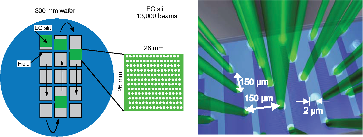 The left part of the figure shows how the movement of the stage affects the writing strategy on the wafer. By moving the stage in a vertical zig-zag order, the MAPPER system with 13,000 electron beams writes a 26-mm () wide stripe during a single vertical scan. By writing these 26-mm wide stripes on the wafer in a vertical zig-zag order, we are actually printing upside down copies of the circuit layout image for the stripes written from the bottom to the top. This could be a problem if a circuit layout image has to be covered by multiple stripes. However, the 26-mm width of a stripe is wide enough to cover most circuits; for example, the previous generation 45 nm Intel Core i7-920 process had a die size of .17 In our MAPPER-like writing strategy, we assume one or multiple copies of the circuit are covered by this 26-mm wide stripe so that we do not have to consider processing different images for each 26-mm wide stripe. Observe that since MAPPER staggers its writing regions in the vertical direction by 150 μm as shown in the right part of Fig. 4, we cannot simply partition the image into blocks and pass each block to the corresponding electron beam writer. The writing strategy of the electron beam writers to create the circuit layout image on the wafer is shown in Fig. 5. Here, the starting position of each electron beam in each writing is marked with a black square and the writing region of each electron beam writer is illustrated as a tall rectangular block where the rows are successively written from the top row to the bottom row in a horizontal zig-zag order. In the HVM setting, whenever an electron beam writer finishes writing a block, it repeats writing the same block until it reaches the end of the wafer region. In the example of Fig. 5, each electron beam writer writes three copies of the blocks (represented by writings #1 to #3), and two copies of the circuit layout image (represented by circuits #1 and #2) are printed on the wafer. Fig. 5The application of the MAPPER writing region to the wafer. The black squares represent the starting positions of the electron beams during each writing, and each tall rectangle within a circuit region illustrates the writing region of the corresponding electron beam writer. 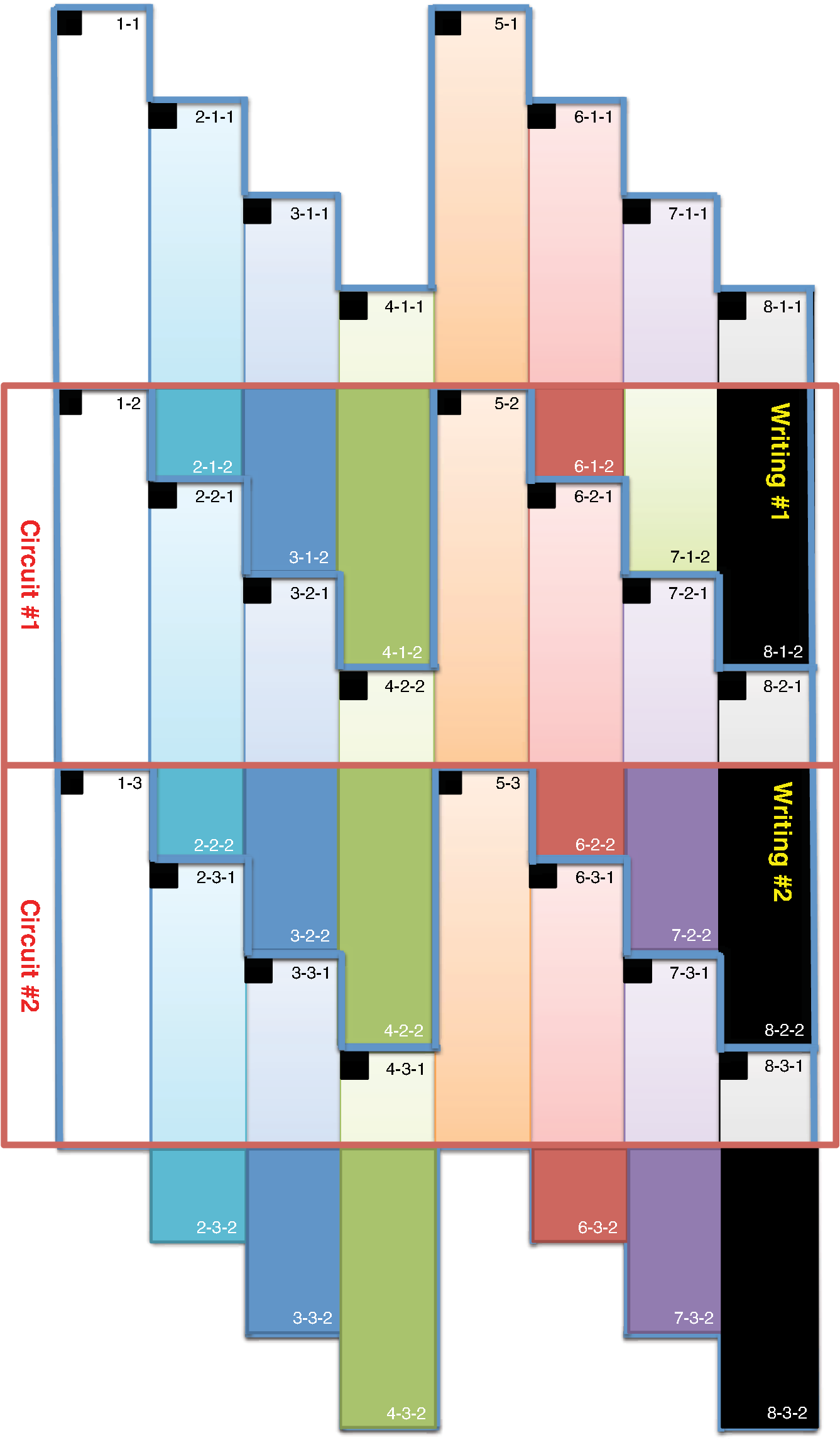 In order to emphasize that some blocks can contribute to two different circuit layout image copies, we used different coloring (light and dark) for the corresponding blocks. For example, block #2 of writing #2 consists of two parts block 2-2-1 and block 2-2-2. While block 2-2-1 is part of circuit #1 along with the second part of block #2 of writing #1 (block 2-1-2), block 2-2-2 is part of circuit #2 along with the first part of block #2 of writing #3 (block 2-3-1). Finally, note that in Fig. 5 all blocks with the same color are identical. That is, blocks 2-1-1, 2-2-1, and 2-3-1 are identical and blocks 2-1-2, 2-2-2, and 2-3-2 are identical. Therefore, the block separation process reinterprets the circuit layout image (or circuit) in the order of the writings of Fig. 5. Figure 6 shows how this process changes the circuit layout image. The top of Figure 6 shows a circuit of Fig. 5, which is a circuit layout image. To obtain the block separated image, we first partition the circuit layout image. Then, we apply circular shifts to the blocks that contribute to two different circuit layout image copies in Fig. 5—the corresponding blocks are blocks #2 to #4 and #6 to #8—so that each block has its electron beam starting point at the top-left corner of the block, as in the second part of Fig. 6. Note that the second part of Fig. 6 corresponds to a writing of Fig. 5. Throughout the discussion of the processes in Fig. 3, when we refer to image blocks we are referring to the blocks in the second part of Fig. 6. The reason that we concentrate on a writing instead of a circuit in the lower part of Fig. 6 is to emphasize the flow of decompressed data to the electron beams. Fig. 6The effects of block separation. The circuit layout image is partitioned and some of the partitioned blocks are rearranged. 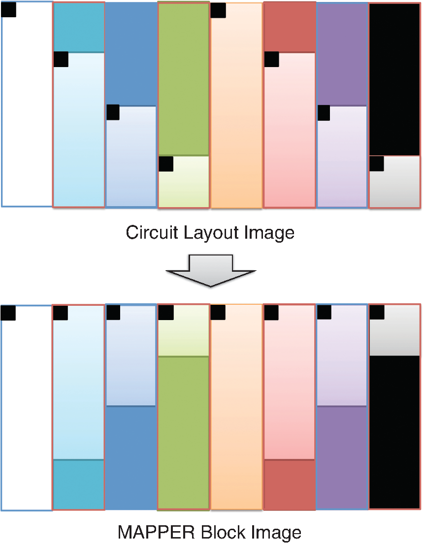 The frequent pattern discovery algorithm, which is described in Sec. 2.2.1, searches each block to discover the frequent patterns used for all blocks. Then each block is a separate input to the forward transformation process. Since it is important to understand the FPR process in order to illustrate the frequent pattern discovery process, in the next subsection we begin by explaining the forward transformation process. 2.2.Forward TransformationOnce the blocks are separated and the frequent patterns are discovered, each block separately goes through the forward transformation process. During the forward transformation process, we first search the image block looking for embeddings of predetermined frequent patterns. Whenever there exists an embedding of a frequent pattern, we replace the embedding with a simple representation. After all of the frequent pattern embeddings are replaced with simple representations, we apply corner transformation to the remaining image where no frequent pattern embeddings were found. Through this process, we handle the regular circuit parts with FPR and the irregular circuit parts with corner transformation. In the following subsections, we will explain in detail the FPR and corner transformation processes. 2.2.1.Frequent pattern replacementFigure 7 offers an overview of FPR. The inputs to the FPR encoder are an image block and the frequent pattern list, and the FPR encoder outputs a matched pattern image and a binary residue image. The FPR process is applied to each image block with the frequent pattern list fixed for all image blocks. The FPR encoder seeks the patterns within the block. Whenever a pattern is matched within the image block, the encoder will replace the first point of the pattern embedding with a pattern symbol and will replace the rest of filled pixels that have been matched with 0’s (or empty). Note that because of the zig-zag writing, the first point of the pattern embedding could be either the top-left corner or the top-right corner of the pattern depending respectively on whether the first row of the pattern is odd or even. For the example in Fig. 7, the first square pattern begins at the first row of the image. Since the first row is written from left to right, the top-left corner of the pattern is replaced with the pattern symbol (gray pixel). Similarly, the second square pattern is found at the second row of the image, and since the second row is written from right to left, the top-right corner of the pattern is replaced with the pattern symbol. Note the output matched pattern can have symbols from the set , where is the symbol used to represent frequent pattern and is the size of the frequent pattern list. Finally, note that when the FPR encoder seeks a pattern, it more precisely searches for the pattern surrounded by empty rows and columns so that the pattern embedding is isolated, i.e., not connected to other polygons. This is necessary to avoid interference with corner transformation and to prevent partial pattern matching, which could result in performance deterioration. Otherwise, the rectangle in the bottom of Fig. 7 can be represented by three squares, which is not desirable. Once the FPR process is applied, the residue image block is passed to the corner transformation process. 2.2.2.Corner transformationThe input to the corner transformation process is the residue image block from the FPR encoder, and the output is the corner transformed image block. As we indicated earlier, like the FPR encoder, the corner transformation process is only processing a block of the layout image at a time. Figure 8 illustrates the corner transformation process. First, we expand the input image block by introducing two empty columns (shown as gray grids in the figure) to surround the input image block in order to handle the zig-zag writing order. Second, we apply horizontal and vertical bitransitional encoding on the expanded image block. This bitransitional encoding marks the pixels (black) where the current pixel value is different from the previous pixel read in the encoding direction, i.e., left to right for horizontal encoding and top to bottom for vertical encoding. Next, we left-shift the even-numbered rows, i.e., the rows that are written from right to left. During this left-shift, the pixels from the surrounding right column could get inside the image area. Finally, we discard the pixels in the expanded columns. By applying this corner transformation, we represent the residue image block using its transitional corners. We call these points transitional corners because they are similar to polygon corners, but they are extracted by transitional coding. Similar to the FPR process, the corner transformation is separately applied to each image block. Fig. 8Corner transformation process of Corner2. The new step (d) accounts for the zig-zag writing strategy. 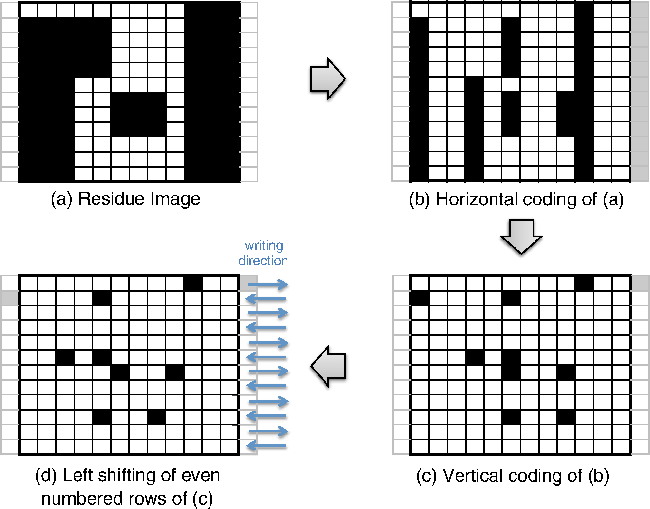 The algorithm is summarized in Algorithm 1. In the algorithm, is the column index of the image block, is the row index of the image block, and we will assume all odd rows are written from left to right and all even rows are written from right to left. Note that is the dimension of the block and is predefined by the MEB DW system. Algorithm 1Corner transformation algorithm.
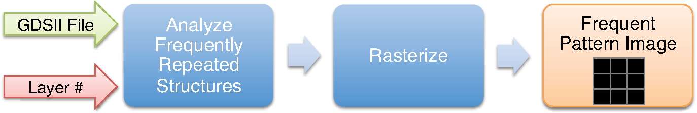
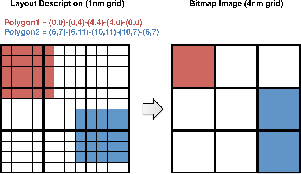
In Ref. 10, we introduced a one-step corner transformation algorithm where pixel is processed as a function of the input pixels (, ), (, ), and (, ). We modified that algorithm so that it applies a left-shift for the even-numbered rows in lines 12 to 16 of Algorithm 1. Observe that the transitional corners can only appear at a polygon corner, right of a polygon corner, left of a polygon corner, below the polygon corner, to the bottom-right of a polygon corner, and to the bottom-left of a polygon corner. By matching isolated patterns during FPR, we guarantee that the transitional corners produced by Algorithm 1 do not overlap with any of the pattern symbols in the matched pattern image block. We sum the pattern matched image block and the corner transformed image block to form the forward transformed image block. By choosing the frequent pattern replacement symbols () to not overlap with corner symbols , we can always separate the matched pattern image block and the corner transformed image block from the forward transformed image block. Finally, after all blocks have been forward transformed, they are input to the flatten pixel stream process, which will be explained in Sec. 2.4, to produce a one-dimensional (encoded) pixel stream. 2.3.Frequent Pattern DiscoveryWe next discuss the generation of the frequent pattern list. This process contains three subprocesses: (1) pattern extraction from the GDSII layout description, (2) candidate pattern generation, and (3) selection of the optimized pattern list. In the following subsections we will offer a detailed description of these procedures. 2.3.1.GDSII pattern extractionIn Ref. 10 we extracted patterns that are frequently used in the entire layout image by seeking the frequently used substructures in the original GDSII layout descriptions since the layout image is rasterized from the GDSII representation. This procedure, which can be effective, is illustrated in Fig. 9.10 However, as illustrated in Fig. 10, this method has shortfalls because some substructures could result in different image patterns depending on the rasterization grid. In Fig. 10, two squares are defined in the layout description (GDSII). When we rasterize the image in a 4-nm grid (Fig. 10, right), we are actually quantizing a block from the 1-nm grid as a single pixel (Fig. 10, left), and we fill the pixel if the number of filled pixels in the original block is at least 8. The rasterized image shown in Fig. 10 (right) has two different polygons, but they came from the same layout description. Furthermore, since we have partitioned the image into blocks, the patterns extracted from the GDSII representation may not have matches. We therefore need to search for frequent patterns within the block images. 2.3.2.Candidate pattern generationIn order to extract patterns that are frequently used for entire image blocks, we search the blocks. We then generate a list of candidate patterns and later determine which among these should be included in the frequent pattern list. In this section, we will discuss the candidate pattern discovery algorithm first described in Ref. 12. As we explained in Sec. 2.2.1, during the FPR process, we match isolated patterns, i.e., we first surround the pattern with empty rows on the top and bottom and empty columns to the left and right. We require that the frequent patterns satisfy the following conditions: (1) the patterns should be defined in a rectangular region, (2) the patterns should never overlap with other patterns, and (3) the patterns should be isolated. First, we will explain how the candidate patterns are generated. Later, we determine which ones will be included in the frequent pattern dictionary. The candidate pattern generating algorithm is shown in Algorithm 2. In the algorithm, is the column index of the image block and is the row index of the image block. Once again note that is the block dimension, which is predetermined by the MEB DW system. Algorithm 2Candidate pattern generation.
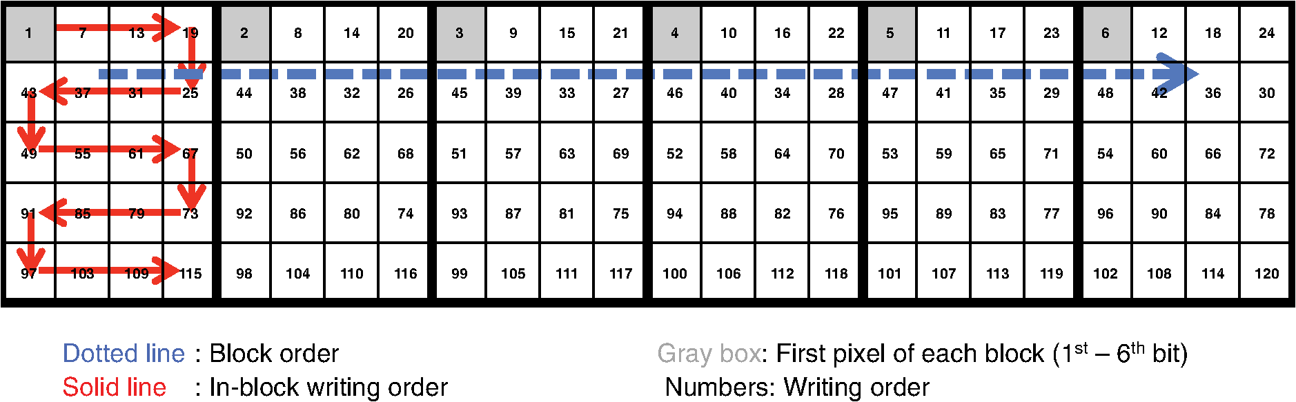
The algorithm starts by picking a pixel from the image block in raster order, i.e., from top to bottom and then from left to right. If the pixel is filled (1), then we define a rectangular region so that all of the filled pixels that are connected to are covered by it (line 5). We then make the rectangular region as the candidate pattern Pattern (line 6) and search the list of candidate patterns PatternList (line 7) to see whether the pattern was already in the list or not. If Pattern was already in the PatternList, we increase its frequency by 1 (line 9). Otherwise, we put Pattern into the PatternList and initialize its frequency to 1 (line 11). Finally, we make sure that the region is not searched again by marking the region in checked (lines 13 to 17), and this prevents the patterns from overlapping. Once again, note that this frequent pattern discovery algorithm is applied separately to each image block. By augmenting the discovered PatternList after processing each block image, we obtain the final candidate pattern list. Moreover, to incorporate the GDSII extracted patterns in Sec. 2.3.1 with the Algorithm 2 patterns, we first run the frequent pattern replacement algorithm of Sec. 2.2.1 on each image block using only the GDSII extracted patterns. We next apply Algorithm 2 to the residue image blocks, which are the block image regions that have not been matched by the frequent pattern replacement process. By combining both the GDSII extracted patterns and the patterns generated using Algorithm 2, we obtain the final candidate pattern list. 2.3.3.Pattern optimizationOnce the candidate patterns are discovered, we analyze them in order to decide which patterns to keep and which patterns to discard. The final patterns will be used as the frequent patterns of the FPR encoder for every image block. As discussed in Ref. 12, there are two parameters that we consider to make this decision. The first parameter is gain, which provides information on what improvement we should expect by using the pattern for the frequent pattern replacement process. Since compression is related to the corners we remove by patterns as well as to the frequency of patterns, we define the gain of pattern as where is the number of corners of pattern and is the frequency of pattern .The second parameter is cost, which shows how much decoder memory is required to keep the pattern in the decoder memory. For the pattern whose dimension is , the decoder usually needs bits of memory to store the pattern. However, we can reduce the cost when the pattern is fully filled. For this case, since we already know that all pixels are filled, all we need to store are the pattern dimensions. We allocate 16 bits for each dimension and a 1 bit flag to specify whether or not the pattern is fully filled. Therefore, the cost of pattern with dimension is defined as follows: To reduce the complexity of the optimization problem, we initially discard the candidate patterns whose gains were less than a preset threshold Threshold. To choose the frequent patterns, we want to where is a binary number indicating whether pattern should be used as a frequent pattern (1) or not (0), and is the decoder memory in bits that can be used to store the frequent pattern dictionary.Equation (1) is an instance of a standard binary integer programming (BIP) problem.18 by setting , , and .Here is the number of candidate patterns. By applying a widely used BIP solver,19 we are able to choose the optimal frequent patterns from the generated candidate pattern list. Finally, note that this optimal frequent pattern set is used during the frequent pattern replacement process of every image block. If we instead use a different frequent pattern set for each image block, we can only assign a fraction of for the frequent pattern replacement of each image block in order to sustain the same decoder memory requirement. That results in discarding some of the large patterns that are widely used in multiple image blocks and, hence, in deteriorating the compression performance. 2.4.Flatten Pixel StreamOnce the forward transformed image blocks are generated, we flatten the forward transformed image blocks into a one-dimensional pixel stream so that the MAPPER system receives an encoded pixel for each block at a time to match the current placement of all of the electron beams. We obtain this stream by gathering the transformed image blocks and reading one pixel from each block in a horizontal zig-zag order. An example of this permutation is shown in Fig. 11 where each block has adimension of and each block is written in zig-zag order. For example, we first read the first (or top-left) pixels of each block in the order of the blocks. Then, we read the second pixels in zig-zag order of each block and continue that until the last pixels in zig-zag order of each block are read. The order in which the pixels are read in this example is marked in the image. Finally, note that this permutation operation inputs the forward transformed image blocks and outputs a long one-dimensional stream to which the following entropy coding schemes will be applied. 2.5.Entropy EncodingWe use the final entropy coding scheme of Refs. 10 and 12 to compress the final flattened stream of pixels. Since the forward transformed images are very sparse, the flattened stream contains long run of zeroes making RLE20 and EOB10 coding efficient to compress it. Moreover, we also find long runs of EOBs as the forward transformed images are very sparse. We use an -ary representation to encode runs of EOBs and an -ary representation to encode runs of zeroes as in Refs. 10 and 12. Observe that the output of RLE+EOB coding can have up to symbols, where is the number of frequent patterns after the pattern optimization process in Sec. 2.3.3 and one symbol is needed for representing the transitional corners shown in Sec. 2.2.2. This symbol string is compressed using arithmetic coding21,22 for further compression. We followed the implementation of arithmetic coding provided by Witten et al.22 For the implementation, the decoder requires four bytes per alphabet symbol, and since we used symbols, bits were required for arithmetic decoding. 3.Decompression AlgorithmThe C2-MEB decoder decompresses the compressed bit stream to write the circuit layout image using the electron beam arrays. Because of the memory constraints of the decoder, the same compressed bit stream is repeatedly retransmitted to the decoder during each writing of an electron beam. The C2-MEB decompression process is illustrated in Fig. 12 and consists of four major blocks: arithmetic decoding, run length and EOB decoding, block reconstruction, and an inverse transformation process block for each electron beam that is directly connected to it. The entire decoder is fabricated on the same silicon as the electron beam writer (controller) array. The first two steps, arithmetic decoding and run length and EOB decoding, reverse the corresponding encoding procedures and output the ()-ary flattened pixel stream of Sec. 2.4. In the block reconstruction process, the input pixel stream is separated into multiple pixel streams, which each correspond to a forward transformed image block. Each such block is converted back into a reconstructed image block, which is passed to an electron beam writer that writes the decoded block onto the wafer as the stage moves. The different image blocks are processed and written in parallel on the wafer by independent inverse transformation processes and the corresponding electron beam writers. The decoder requires bits of cache for each inverse transformation process block to keep intermediate information for the row-by-row decoding of each block, bits of memory for the frequent pattern dictionary, and bits for arithmetic decoding, where width is the width of the image block, is the number of total frequent patterns, and are RLE/EOB parameters. 3.1.Block ReconstructionSince arithmetic and RLE+EOB decoding are well understood in data compression, we will next discuss the reconstruction of the forward transformed image blocks of Sec. 2.2 from the flattened pixel stream of Sec. 2.4. As illustrated in Fig. 13, we can achieve this by wiring each symbol of the flattened pixel stream to the corresponding inverse transformation data queue. Fig. 13Reconstructing the forward transformed image blocks from the flattened stream. The decoder places each incoming stream symbol into the appropriate inverse transformation data queue. All of the symbols in a queue are rearranged into a block that undergoes the inverse transformation process to produce a decoded image block. 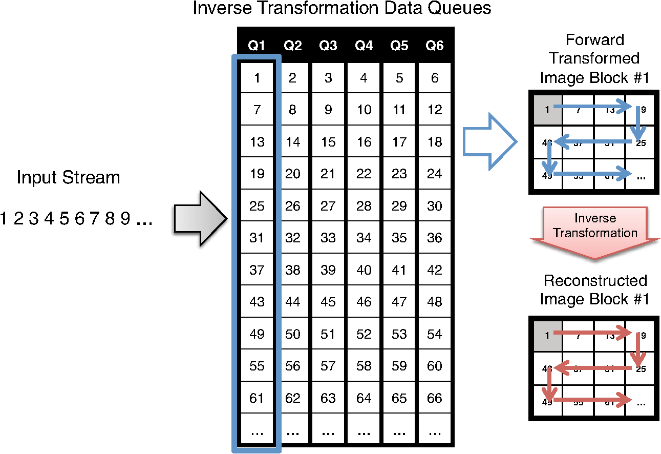 In the example shown in Fig. 13, we are assuming there are six electron beam writers and six inverse transformation processes working simultaneously for the system. The information stored in the inverse transformation data queue is passed onto the inverse transformation process where each row of a forward transformed image block is reconstructed and decoded as a row of the reconstructed image block. Since each inverse transformation process block is connected to the corresponding electron beam writer, each reconstructed row is passed to the electron beam writer to be written on the wafer. 3.2.Inverse TransformationInverse transformation is applied to each forward transformed image block to reconstruct the original image block. The reconstructed image block is forwarded to the associated electron beam writer. The inverse transformation performs frequent pattern reconstruction and inverse corner transformation. Recall that the frequent patterns are encoded using symbols while the transitional corners are marked by the symbol 1. The bottom half of Fig. 12 shows the detailed hardware architecture of an inverse transformation block. As illustrated in the figure, both the inverse corner transformation and the frequent pattern reconstruction processes require a row buffer to keep track of the previous row’s status. The frequent pattern reconstruction process also requires a frequent pattern dictionary. Note that this frequent pattern dictionary is shared among all of the inverse transformation blocks. Observe that since the electron beams write a pixel of each image block at the same time, synchronization is needed among the inverse transformation processes. Here we have the inverse transformation processes produce a row of each reconstructed image block in parallel. We next explain the operation of the inverse corner transformation and the frequent pattern reconstruction processes for an image block. 3.2.1.Inverse corner transformationThe inverse corner transformation uses pixels from the previous row and column to decode the current pixel. We designed the decoder to decode the input corner transformed image block in a row-by-row manner instead of in its entirety in order for this process to be compatible with the restricted memory available to the hardware decoder. The inverse corner transformation process is as follows: First, the decoder reads the input corner transformed image block in a zig-zag order. The zig-zag order is the same as raster order except that it reads the even rows from right to left. Second, the decoder processes the current pixel by checking the status of the row buffer (BUFF). The row buffer is used to store the status of the previous (decoded) row. It uses two symbols, 0 and 1, to represent its status, and hence, the buffer requires width bits of memory. “0” means no transition while “1” means transition and indicates the starting/ending point of a vertical line. Third, whenever the read symbol is a transitional corner point (“1”), the decoder starts reconstructing a horizontal line by setting the horizontal line fill flag (Fill) until it reads another transitional corner point from the input row and resets the horizontal line fill flag. For the even rows, this line is written from right to left, while it is written from left to right for the odd rows. Fourth, for every new horizontal line created by the transitional corners, the row buffer (BUFF) is updated so that the decoder can take the status of the current row into account while reconstructing the next row. Note that because we are dealing with transitional corners, a horizontal line starts from a transitional corner point and ends one pixel before the pairing transitional corner point. In Fig. 8, step (d) is applied to sustain the same decoding rule for the even rows. If the encoder did not left-shift the even rows, then in order to reconstruct the horizontal lines of those rows, the decoder has to start a horizontal line one pixel after a transitional corner point and end it at the pairing transitional corner point. However, there could be a problem reconstructing the horizontal line of the even rows when the first pixel of the row (i.e., the rightmost pixel) has to be filled. Since there is no pixel to the right of the rightmost pixel, the reverse line from right to left cannot be reconstructed using this decoding rule. By inserting an empty right column and allowing the transitional corners to appear there and applying left-shifts to the even rows as in step (d) of Fig. 8, we can always reconstruct horizontal lines by starting from a transitional corner point and ending it one pixel before the corresponding transitional corner point following the row direction. Because the inverse corner transformation rule is independent of the row direction, we have to make sure that the column index matches the row direction. Algorithm 3 describes the inverse corner transformation process. We assume the inverse corner transformation decoder can randomly access the entire row buffer and the input corner transformed image block is read in a zig-zag order. Note that the operation is a binary XOR operation and is only applied to binary summands. Algorithm 3Inverse corner transformation.
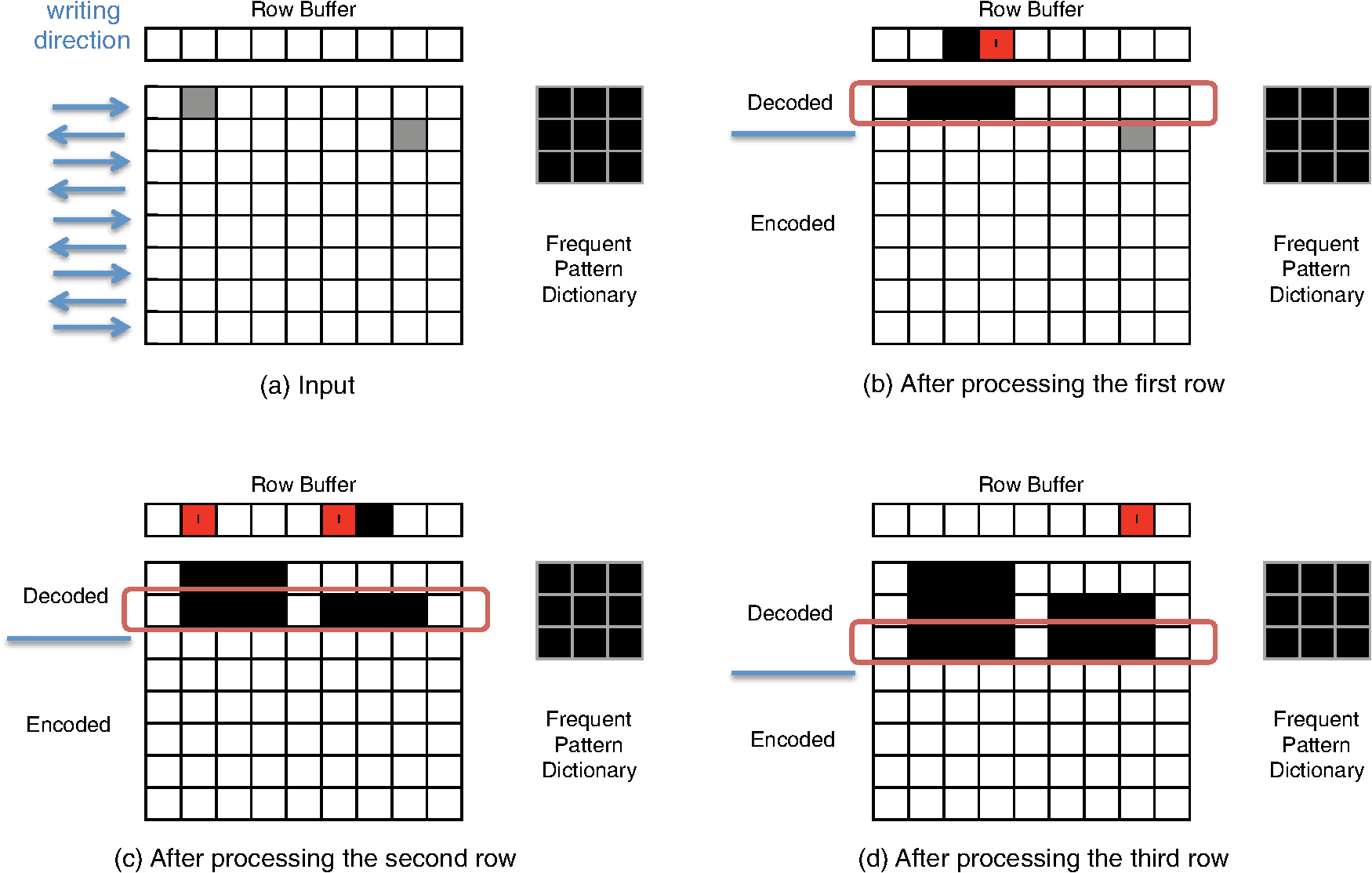
In Algorithm 3, the horizontal fill flag (Fill) is initialized for every row (line 4). Then we check the row number and update the column index (lines 6 to 10). If the row is odd numbered, then the column index starts from 1 to (lines 6 and 7), while the order is reversed (from to 1) if the row number is even. We update the column index if the row number is even (lines 8 to 10). Lines 11 to 13 process the buffer. If the buffer is filled, i.e., if there is a vertical fill, then the corresponding pixel is filled. If the input pixel (read in zig-zag order) is a transitional corner (“1”), the decoder changes the status of the horizontal fill flag (lines 14 to 16). Finally, depending on the horizontal fill flag (Fill), the output pixel (line 17) and the buffer (line 18) are updated if necessary. If the input pixel is “0,” the decoder makes no horizontal/vertical changes to the image, but fills the output pixels and updates the buffer according to the fill status. 3.2.2.Pattern reconstructionIf the decoder finds symbols within the forward transformed image block, it starts the pattern reconstruction process. First, it reconstructs the first row of the corresponding pattern according to its writing order. If the decoder is processing an odd row, it will reconstruct the pattern row from left to right and otherwise it will reconstruct the pattern row from right to left. Second, it updates the corresponding buffer with the following string: Here $ is a special symbol used to indicate the start of frequent pattern replacement. If pattern of dimension is to be reconstructed, then Pattern# is a -bit binary representation of and Row# is a -bit binary representation of one less than the remaining number of pattern rows the decoder has to reconstruct. Because Pattern# determines which frequent pattern the decoder needs to reconstruct (and its dimension), and Row# determines which row of the corresponding pattern it has to reconstruct, the decoder can reconstruct the pattern. We could alternatively use base-3 logarithms, but that would complicate the decoding hardware. Note that this stream is updated depending on the writing direction of the next row. An example of the frequent pattern reconstruction process is demonstrated in Fig. 14. When the first row is decoded, we update the row buffer in the reverse direction starting at the fourth column because the next row is written from right to left and the pattern involves the second, third, and fourth columns. The stream is represented as in the reverse direction because there is only one frequent pattern defined in the dictionary making . (In Fig. 14, the $’s are represented by red pixels and the 1’s are represented by black pixels.) In the next row, the decoder has to process two more rows of the pattern. When the second row is decoded, since the writing order of the next row is from left to right and since we need to write one more row to the first pattern, the buffer of the first pattern is updated to in the forward direction. Similarly, the buffer of the second pattern is updated to . Finally, when the third row is decoded, we reinitialize the buffer of first pattern to [0 0] to indicate that the frequent pattern reconstruction is complete. In order to combine this frequent pattern reconstruction and the inverse corner transformation, the inverse transformation decoder requires bits for the row buffer for each inverse transformation block and bits to store the pattern dictionary. Given that the forward transformed image is a ()-ary array with dimension , this buffer requirement is comparatively small. 4.Experimental ResultsWe tested the algorithm on two custom circuits—a memory circuit and a binary frequency shift keying (BFSK) transmitter circuit used for testing Corner2.10,12 The memory core was targeting 500-nm lithography technology containing 13 layers of repeated memory cell structure. The custom-designed BFSK transmitter was targeting 250-nm lithography technology containing 19 layers of mostly irregular features. We scaled these images to the point where their minimum features were small rectangles (with less than a dozen pixels) to simulate the MAPPER environment. Most parts of C2-MEB were written in C/C++ with OpenMP support for processing the forward and inverse transformation processes in parallel. For the decoding process, the inverse transformation processes are synchronized so that the same writing row of each was processed in parallel. Because C2-MEB blocks can be processed independently, we applied parallel processing for faster encoding/decoding speed. The binary integer programming part was written in MATLAB using the MATLAB function bintprog.19 All of the experiments ran on a laptop computer having a 2.53 GHz Intel Core 2 Duo CPU and 4 GB RAM. We applied C2-MEB and compared the results with Corner2-BIP (C2-BIP),12 Corner2 (C2-ORG),10 and BC4.7 While C2-BIP, Corner2, and BC4 were applied to the entire layout image, C2-MEB was applied in a block fashion. We set the MAPPER block size to be because the MAPPER writing region is a width-2 μm stripe on a 2.25-nm grid.6 Here, height is the height of the circuit layer image, which was 17,816 for the memory circuit and 31,624 for the BFSK circuit. In the following subsections we show the compression results for both the memory and BFSK circuits on the MAPPER system. In the following subsections, we defined the compression ratios to be Note that the total compression ratio is not the average of the preceding compression ratios, but the net average, which is defined as To compare the result with C2-BIP, we used the same , , and settings as in Ref. 12. 4.1.Memory CircuitTables 1 and 2 show the experimental results for the memory circuit when the MAPPER block separation was applied. Because of the block partitioning, C2-MEB had 37.3 and 14.9% smaller compression ratio than C2-BIP and C2-ORG, respectively, which operated on the full layout image. However, C2-MEB was still 2.9 times better than BC4 as shown in Table 1. The block partitioning resulted in fewer pattern matches and introduced more corners in the block boundaries. Moreover, the flattening process also deteriorated the RLE+EOB encoding by segmenting long run of zeroes into smaller pieces. However, because Corner2-variations have better layout image modeling, C2-MEB still resulted in better compression performance than BC4. Table 1Compression ratio (x)—Memory array (block size: 888×17,816).
Table 2Encoding/decoding time (s)—Memory array.
On average, C2-MEB encoding was 3% (or 0.3%) faster than C2-BIP (or C2-ORG) and 50.8 times faster than BC4 as shown in Table 2. While C2-MEB generated more candidate patterns due to block truncation, which slowed down the encoding process, it became faster than C2-BIP and C2-ORG because of parallel processing. However, C2-MEB encoding could be further accelerated by using more parallelization. Since the Intel Core 2 Duo CPU only supports running four threads simultaneously, we were not able to take advantage of processing all blocks in parallel. Distributed computing over the grid or an application of GP-GPU-based parallel processing might enable this. On average, C2-MEB decoding was 17% (or 13%) slower than C2-BIP (or C2-ORG), while it was 16.0 times faster than BC4 as shown in Table 2. Our decoding time results do not include the time to reverse the flattening process because this procedure would be unnecessary in a hardware implementation. The process was only used to verify that the reconstructed image matches with the input image. Furthermore, similar to the encoding time, we expect the decoding time to be further reduced when full parallelization is applied. Considering this as a compress-once-and-decode-multiple-times application, C2-MEB is more realistic than C2-BIP and C2-ORG in that it takes advantage of multiple electron beams, and it offers better compression than BC4. 4.2.BFSK CircuitTables 3 and 4 show the experimental results for the BFSK circuit when the MAPPER block separation was applied. Like the memory circuit, C2-MEB had a 28.4% smaller compression ratio than C2-BIP and a 25.2% smaller compression ratio than C2-ORG. This is mainly due to the new corners introduced and the shortened runs of zeroes due to block separation. However, C2-MEB still offered a 3.4 times better compression ratio than BC4. On average, C2-MEB was 58% slower than C2-BIP and 79% slower than C2-ORG, while it was 109.0 times faster than BC4. Compared to the memory circuit result, the improvements in encoding speeds were because more candidate patterns had to be generated even though not so many of them were used. Similarly, C2-MEB was 18% slower than C2-BIP and 14% slower than C2-ORG, while it was 26.1 times faster than BC4. However, this was because we could run only four inverse transformation processes in parallel, which could be further improved with the help of massively parallel computing. Table 3Compression ratio (x)—BFSK circuit (block size: 888×31,624).
Table 4Encoding/decoding time (s)—BFSK circuit.
5.ConclusionIn this paper, we have modified Corner2 for MAPPER-like systems. Although its compression performance was inferior to that of C2-BIP12 due to block processing, it is better suited to MEB DW systems because it incorporated the actual writing strategy and because the inverse transformation process can be parallelized for higher throughput. Moreover, the performance of C2-MEB was still far better than that of BC4. Hence handling regular circuit parts using dictionary-based compression and irregular circuit parts using corner-based (or vertex-based) representation as in Corner2 is far more effective than handling regular circuit parts using Lempel-Ziv-based compression and irregular circuit parts using prediction-based compression as is done in BC4. The decoder needs to be implemented in hardware, and we showed that the Corner2 inverse transformation decoder along with the RLE+EOB decoder required only 2% of a Xilinx Spartan 3E field-programmable gate array board even when using 5 kbytes of decoder cache.13 The C2-MEB decoder consists of an arithmetic decoder, RLE+EOB decoder, and 13,000 inverse transformation blocks with each inverse transformation block smaller than those we introduced in Ref. 13. Each inverse transformation block consists of simple operations such as comparisons, branches, XORs, and binary arithmetic. Since a GPU core can handle these operations and more advanced operations, we argue that the dedicated inverse transformation core will be much smaller than a GPU core. The row buffer requirement for each inverse transformation block is bits, where is the block width. Therefore, the entire C2-MEB system supporting 13,000 electron beams will require of cache. Since current GPUs have cores23 and previous generation Intel CPUs have 8 MB of cache,17 the entire C2-MEB decoder can be built using current silicon technologies. We have two concerns regarding this algorithm. First, we do not have an efficient hardware implementation for the arithmetic decoder, making the final arithmetic encoding less suitable for the purpose. We can tackle this issue by using other standard compression techniques and trading off part of the compression ratio for an efficient hardware decoder; since C2-MEB has about three times better compression performance than BC4, there is some room for this trade-off. Second, adjustments to the algorithm will be necessary to account for e-beam proximity correction (EPC).24 We expect that EPC layout images will not have linear boundaries. Nevertheless, some combination of frequent pattern replacement with a loose matching and a way to handle errors will be useful. This is the next major direction of this line of research. AcknowledgmentsThe work of the second author was supported in part by the National Science Foundation grants CCF-1017303 and ECCS-1201994. ReferencesB. Lin,
“Future of multiple-e-beam direct-write systems,”
Proc. SPIE, 8323 832302
(2012). http://dx.doi.org/10.1117/12.919747 PSISDG 0277-786X Google Scholar
N. ChokshiY. ShroffW. G. Oldham,
“Maskless extreme ultraviolet lithography,”
J. Vac. Sci. Technol. B, 17
(6), 3047
–3051
(1999). http://dx.doi.org/10.1116/1.590952 JVTBD9 0734-211X Google Scholar
V. DaiA. Zakhor,
“Lossless compression of VLSI layout image data,”
IEEE Trans. Image Process., 15
(9), 2522
–2530
(2006). http://dx.doi.org/10.1109/TIP.2006.877414 IIPRE4 1057-7149 Google Scholar
V. Dai,
“Data compression for MEBL systems: architecture, algorithms, and implementation,”
Department of Electrical Engineering and Computer Science, University of California, Berkeley,
(2008). Google Scholar
P. Petricet al.,
“REBL nanowriter: reflective electron beam lithography,”
Proc. SPIE, 7271 727107
(2009). http://dx.doi.org/10.1117/12.817319 PSISDG 0277-786X Google Scholar
E. Slotet al.,
“MAPPER: high throughput maskless lithography,”
Proc. SPIE, 6921 69211P
(2008). http://dx.doi.org/10.1117/12.771965 PSISDG 0277-786X Google Scholar
H. Liuet al.,
“Reduced complexity compression algorithms for direct-write maskless lithography systems,”
J. Micro/Nanolithogr. MEMS MOEMS, 6
(1), 013007
(2007). http://dx.doi.org/10.1117/1.2435202 1932-5150 Google Scholar
G. CramerH.-I. LiuA. Zakhor,
“Lossless compression algorithm for REBL direct-write e-beam lithography system,”
Proc. SPIE, 7637 76371L
(2010). http://dx.doi.org/10.1117/12.845506 PSISDG 0277-786X Google Scholar
J. YangS. A. Savari,
“A lossless circuit layout image compression algorithm for maskless lithography systems,”
in Proc. of the 2010 Data Compression Conf.,
109
–118
(2010). Google Scholar
J. YangS. A. Savari,
“A lossless circuit layout image compression algorithm for maskless direct write lithography systems,”
J. Micro/Nanolithogr. MEMS MOEMS, 10
(4), 043007
(2011). http://dx.doi.org/10.1117/1.3644620 1932-5150 Google Scholar
F. KrecinicS.-J. LinJ. J. H. Chen,
“Data path development for multiple electron beam maskless lithography,”
Proc. SPIE, 7970 797010
(2011). http://dx.doi.org/10.1117/12.881010 PSISDG 0277-786X Google Scholar
J. YangS. A. Savari,
“Improvements on Corner2, a lossless layout image compression algorithm for maskless lithography systems,”
Proc. SPIE, 8352 83520K
(2012). http://dx.doi.org/10.1117/12.923205 PSISDG 0277-786X Google Scholar
J. YangX. LiS. A. Savari,
“Hardware implementation of Corner2 lossless compression algorithm for maskless lithography systems,”
Proc. SPIE, 8323 83232O
(2012). http://dx.doi.org/10.1117/12.917581 PSISDG 0277-786X Google Scholar
E. PlatzgummerC. KleinH. Loeschner,
“eMET POC: realization of a proof-of-concept 50 keV electron multibeam mask exposure tool,”
Proc. SPIE, 8166 816622
(2011). http://dx.doi.org/10.1117/12.895523 PSISDG 0277-786X Google Scholar
J. YangS. A. Savari,
“Transform-based lossless image compression algorithm for electron beam direct write lithography systems,”
Recent Advances in Nanofabrication Techniques and Applications, 95
–110 InTech, Rijeka, Croatia
(2011). Google Scholar
S. M. Rubin, Computer Aids for VLSI Design, 2nd ed.Addison-Wesley, Boston
(1987). Google Scholar
“Intel Core i7-920 processor specifications,” http://ark.intel.com/products/37147/Intel-Core-i7-920-Processor-(8M-Cache-2_66-GHz-4_80-GTs-Intel-QPI Google Scholar
L. A. Wolsey, Integer Programming, Wiley-Interscience, New York
(1998). Google Scholar
MathWorks, “bintprog,”
http://www.mathworks.com/help/toolbox/optim/ug/bintprog.html Google Scholar
S. Golomb,
“Run length encodings,”
IEEE Trans. Inf. Theory, 12
(3), 399
–401
(1966). http://dx.doi.org/10.1109/TIT.1966.1053907 IETTAW 0018-9448 Google Scholar
A. MoffatR. M. NealI. H. Witten,
“Arithmetic coding revisited,”
ACM Trans. Inf. Syst., 16
(3), 256
–294
(1998). http://dx.doi.org/10.1145/290159.290162 1046-8188 Google Scholar
I. H. WittenR. M. NealJ. G. Cleary,
“Arithmetic coding for data compression,”
Commun. ACM, 30
(6), 520
–540
(1987). http://dx.doi.org/10.1145/214762.214771 CACMA2 0001-0782 Google Scholar
Nvidia GeForce GTX 690 GPU Specification http://www.geforce.com/hardware/desktop-gpus/geforce-gtx-690/specifications Google Scholar
F. Yesilkoyet al.,
“Implementation of e-beam proximity effect correction using linear programming techniques for the fabrication of asymmetric bow-tie antennas,”
Solid State Electron., 54
(10), 1211
–1215
(2010). http://dx.doi.org/10.1016/j.sse.2010.05.009 SSELA5 0038-1101 Google Scholar
Biography Jeehong Yang received his BS degree in electrical engineering from Yonsei University, Seoul, Korea, in 2003. He received his MS and PhD degrees in electrical engineering and computer science from the University of Michigan-Ann Arbor in 2005 and 2012. He was involved in developing various data compression algorithms (text, audio, image, and video) and parallel processing algorithms. He is currently working at Qualcomm Technologies Inc.  Serap A. Savari is an electrical engineer at Texas A&M University. She received her SB and SM degrees in electrical engineering, her SM degree in operations research, and her PhD degree in electrical engineering and computer science, all from the Massachusetts Institute of Technology. She was with the Computer Sciences Research Center at Bell Laboratories, Lucent Technologies from 1996 to 2003 and with the University of Michigan, Ann Arbor from 2004 to 2007. She was an associate editor for source coding for the IEEE Transactions on Information Theory from 2002 to 2005. She was the Bell Labs representative to the DIMACS council from 2001 to 2003 and has served on the program committees for numerous conferences and workshops in data compression and in information theory.  H. Rusty Harris earned his BS in engineering physics, and master’s and PhD in electrical engineering at Texas Tech University. He previously worked in technology development in Advanced Micro Devices and was assigned to SEMATECH. He is currently an assistant professor in electrical engineering and physics at Texas A&M University. |
|||||||||||||||||||||||||||||||||||||||||||||||||||||||||||||||||||||||||||||||||||||||||||||||||||||||||||||||||||||||||||||||||||||||||||||||||||||||||||||||||||||||||||||||||||||||||||||||||||||||||||||||||||||||||||||||||||||||||||||||||||||||||||||||||||||||||||||||||||||||||||||||||||||||||||||||||||||||||||||||||||||||||||||||||||||||||||||||||||||||||||||||||||||||||||||||||||||||||||||||||||||||||||||||||||||||||||||||||||||||||||||||||||||||||||||||||||||||||||||||||||||||||||||||||||||||||||||||||||||||||||||||||||||||||||||||||||||||||||||||||||||||||||||||||||||||||||||