|
|
1.IntroductionScaling down of semiconductor devices has required continual improvement in photolithography techniques such as immersion lithography and double-patterning lithography. “Directed self-assembly” (DSA), which combines self-assembling materials with lithographically defined pre-patterns, has been widely studied.1–6 According to the International Technology Roadmap for Semiconductors 2012, DSA is a potential candidate as a next-generation lithography technique for 16-nm half-pitch and beyond.7 Two key advantages of DSA are its capability of making a nanoscale structure and its cost effectiveness. One promising approach for DSA is the use of diblock copolymers, which consist of two chemically different immiscible polymers connected at one end of each polymer chain. During DSA, a diblock copolymer is segregated into two polymer phases on the surface of a substrate in a chemically or morphologically controlled manner.8,9 The morphological structure of a phase-separated diblock copolymer, such as alternating lamellae, hexagonally packed cylinders, and spherical domains in body-centered lattice, depends on the interaction parameters, the molecular weight, and the composition of the two polymer blocks.10,11 Among the variety of diblock copolymers, poly(styrene-block-methyl methacrylate) (PS-b-PMMA) has been extensively studied as a potential candidate for DSA. It has been reported that PS-b-PMMA forms microphase-separated structures smoothly, because the value of glass-transition temperatures of PS and PMMA are close.12 One important issue in the development of DSA with diblock copolymers is to produce high-etching selectivity of PMMA to PS (hereafter “PMMA/PS etching selectivity”). This process is used to fabricate a high-quality PS mask for subsequent etching processes. One standard approach for achieving high PMMA/PS etching selectivity is to use argon–oxygen-based plasmas.13–15 Several other plasma-etching processes have been reported.16–18 In plasma etching, ions and radicals generated in the plasma react with the material on the wafer. In 1983, Gokan et al. researched the reaction of organic polymers with only ions by using either argon or oxygen ion-beam etching (IBE) and showed that the etching rate of organic polymers changes when the carbon and oxygen contents in the polymers are changed.19 They obtained PMMA/PS etching selectivity of around 2.0 in the case of etching with either argon or oxygen ion beams. Recently, Ting et al. compared the PMMA/PS etching selectivities of five different plasmas, namely argon plasma, oxygen plasma, argon-oxygen mixed plasma, tetrafluoromethane plasma, and oxygen-trifluoromethane mixed plasma.13 They reported that the argon-oxygen mixed plasma is the best choice for PMMA etching, because it produces reasonably high PMMA/PS etching selectivity of 2.04 and a smooth PS mask surface. The argon-oxygen mixed plasma is thus regarded as a promising candidate for selective PMMA/PS etching. They also reported that using argon plasmas, which produce the highest etching selectivity of around 7, are accompanied by a visibly roughened surface. However, these reports contain little information on the etching mechanism of PMMA. Given the above-described background, in this work the underlying mechanism of selective PMMA etching in argon-oxygen-based plasmas [namely inductively coupled plasmas (ICPs) composed of argon gas only, oxygen gas only, or an argon-oxygen gas mixture] was clarified. It was found that the addition of a small amount of oxygen to argon improves PMMA/PS etching selectivity. A simple model for the improvement in selectivity (which is consistent with the observed etching characteristics) is proposed. The argon-oxygen gas mixture was used to fabricate a high-quality PS mask from a PS-b-PMMA fingerprint pattern. 2.Experimental ProcedureTwo blanket films, made of PMMA homopolymer (P4078-MMA) and PS homopolymer (P1758-S) purchased from Polymer Source Inc., Dorval, Quebec, Canada were used to evaluate the etching depth of each polymer and PMMA/PS etching selectivity. Number-average molecular weights of both PMMA and PS blanket films are 11,500. The two blanket films were spin coated from toluene solution (2 wt%) at 1000 rpm on silicon substrates to thicknesses of 100 nm. Three kinds of PS-b-PMMA fingerprint patterns (P8966-SMMA, P8533-SMMA, and P5539-SMMA) purchased from Polymer Source Inc.—with target full pitches of 25.5, 41.0, and 77.0 nm—were also deposited on substrates as described below, and the patterns were etched to form PS masks. The number-average molecular weights of PS/PMMA in each PS-b-PMMA pattern were for the 25.5-nm full-pitch pattern, for the 41.0-nm full-pitch pattern, and for the 77.0-nm full-pitch pattern. Before forming the PS-b-PMMA patterns, the silicon substrates were cleaned in a 7:3 mixture of sulfuric acid and hydrogen peroxide (piranha solution) at 80°C for 10 min and rinsed with deionized water. Hydroxyl-terminated PS-r-PMMA (P6469B-SMMAranOHT), purchased from Polymer Source Inc., were spin coated on the cleaned silicon substrates with toluene solution (0.5 wt%) at 2000 rpm. Then, the hydroxyl-terminated PS-r-PMMA was grafted onto the silicon substrates by annealing in vacuum at 170°C for 72 h. After annealing, the substrates were rinsed twice with toluene to remove any unreacted polymers, and PS-r-PMMA brush was formed on the substrates. Thin films of lamellar-forming PS-b-PMMA were coated on the PS-r-PMMA brush and annealed at 230°C for 6 h. Then, PS-b-PMMA fingerprint patterns were formed on the substrates. The blanket films and fingerprint patterns were etched in an ICP etching system for 300-mm wafers, in which a two-turn coil, connected to a 13.56-MHz source power, was located above an dome. A faraday shield covering the dome is connected to a source-power line. The energy of incident ions into the internal surface of the dome is adjusted by changing the voltage of the faraday shield (FSV). The detail of the equipment is described elsewhere.20 The source power was varied from 100 to 1000 W, and FSV was 50 or 400 V. An optical emission spectroscopy apparatus was installed in the view port on one side of the chamber wall. The bottom electrode of the ICP system was connected to an 800-kHz bias power supply to control the energy of ions. The bias power ranges from 0 to 10 W. Argon, oxygen, and an argon-oxygen mixture were used as discharge gases. Process pressure was controlled by using a variable-conductance gate valve. The process pressure was varied from 0.5 to 2.0 Pa. In the argon plasma, the main etching mechanism is physical sputtering by argon-ion bombardment. However, it is expected that a small amount of oxygen radicals enhances the etching rates of polymers, because the dome is also bombarded by argon ions and oxygen impurities (which originate from the dome) and are mixed into the argon plasmas. IBE with argon ions was used to evaluate the etching rate of PMMA. When IBE is used, the etching-rate change due to oxygen incorporation is avoided, because the PMMA is etched only by ions when the PMMA and the plasma (i.e., ion source) are separated. Therefore, hardly any oxygen radicals arrive at the surface of the PMMA even when a small amount of oxygen radicals is produced in the ion source. Etching depth was measured by stylus profilometer (Tencor P-11) at scan speed, 50-Hz sampling rate, and 5-mg stylus force. The etching depth was measured five times for each sample. The etching depth was estimated by averaging the five etching-depth data. The compositional change in the surface of the PMMA during argon-ion etching was evaluated by x-ray photoelectron spectroscopy (XPS) equipped with an argon-ion gun (Theta Probe manufactured by Thermo Fisher Scientific, East Grinstead, West Sussex, UK). The XPS analysis, with spatial resolution of 400 μm, was performed at a 54 deg take-off angle by using a monochromated Al x-ray source. Acceleration voltage of the ion gun was either 500 V or 3 kV, while ion current was kept at . 3.Results and Discussion3.1.PMMA Etching in Argon Plasma or Oxygen PlasmaThe etching rates and the PMMA/PS etching selectivity in argon or oxygen plasmas are listed in Table 1. In the case of both plasmas, etching rates of PMMA are higher than those of PS. In the case of argon plasma, selectivity is 3.9, which is higher than that in the case of oxygen plasma, which is 1.7. This result, namely that PMMA/PS etching selectivity in argon plasma is higher than that in oxygen plasmas, is consistent with recent experimental measurements reported by Liu et al.17 and Ting et al.13 Table 1Etching selectivity of PMMA/PS in argon and oxygen plasmas (100-W source power, 50-V FSV, 10-W bias power, 2.0-Pa gas pressure, and 120-s etching time).
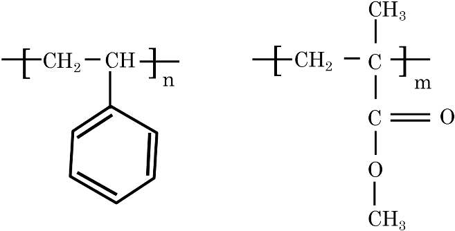
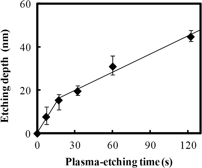
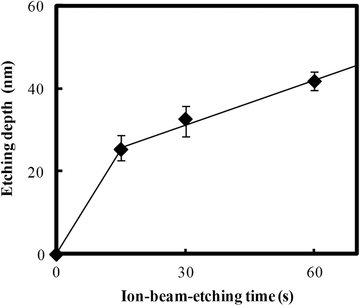
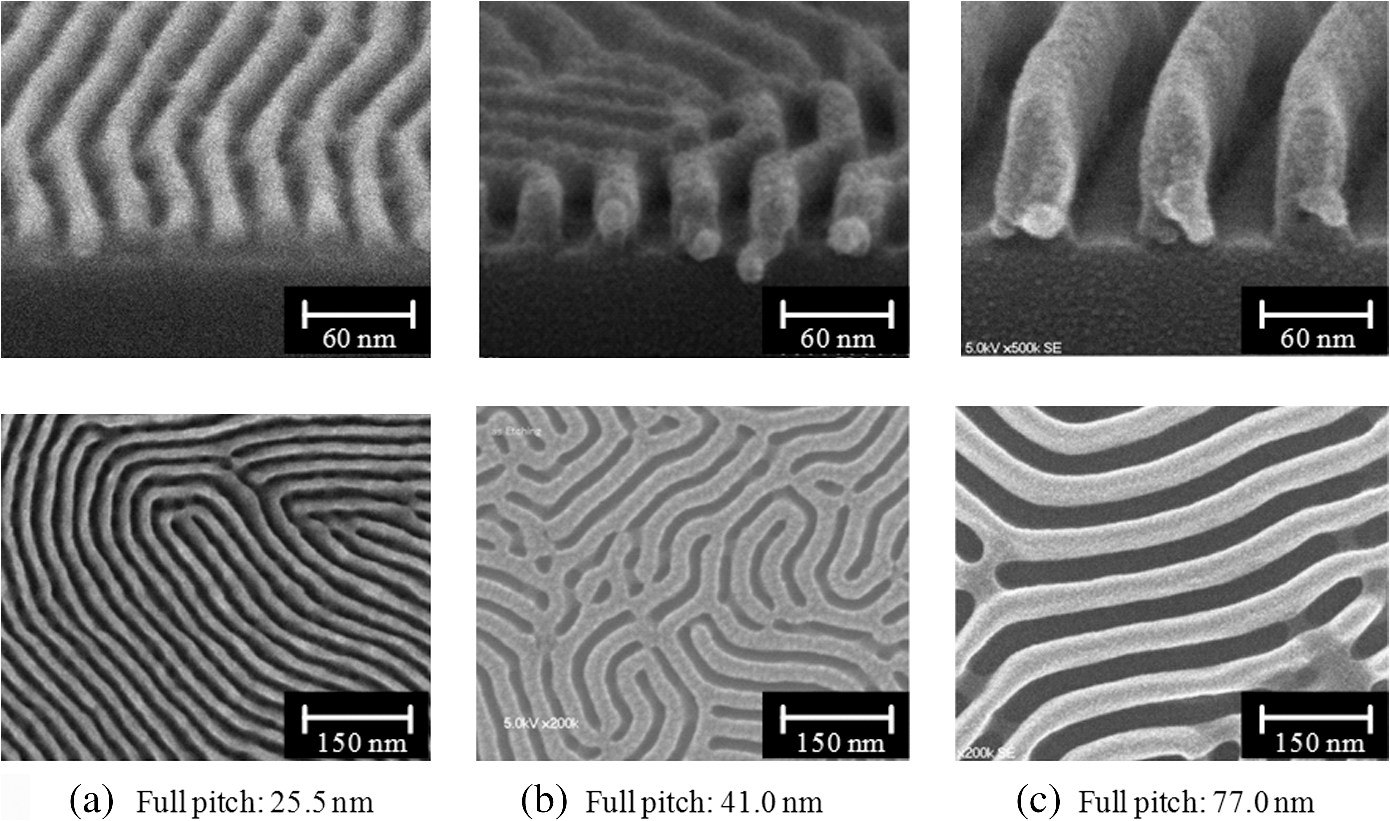
In argon plasmas, physical sputtering by argon ions is the main mechanism of etching. The high-etching selectivity in argon plasmas is probably due to the difference between the molecular structures of PS and PMMA. The schematics of the molecular structures of PS and PMMA are illustrated in Fig. 1. The molecular structure of PS includes benzene rings, which enhance the durability of polymers against etching. The enhancement in the durability is due to electrons in these benzene rings.21 In contrast, the molecular structure of PMMA includes oxygen atoms instead of benzene rings. The oxygen atoms enhance the etching rate, because carbon atoms in polymers are easily volatized when oxygen atoms are present. This difference in the molecular structures of PS and PMMA is the cause of their different etching rates. To investigate the argon plasma process in detail, time dependence of etching depth was evaluated (Fig. 2). The PMMA etching rate is reduced by more than one half after the etching depth exceeds 15 nm. If PS etching rate was constant regardless of etching depth, this result (i.e., over 50% reduction in etching rate) explains the low-etching selectivity and pattern degradation in formation of a PS mask with thickness of more than 20 nm. 3.2.Effect of Oxygen Impurities on PMMA EtchingOne possible cause for the decrease in PMMA etching rate in argon plasma is the change in the amount of oxygen from the dome or the change in the amount of residual oxygen impurities, such as water or other adsorbates, on the chamber wall or on the surface of the wafer. The amount of oxygen incorporation is expected to be especially high immediately after plasma ignition. The time dependence of oxygen-emission intensity was determined by using a bare silicon wafer under argon plasma at high-source power (1000 W) and high-FSV (400 V) etching conditions (Fig. 3). According to the figure, the intensity of oxygen emission decreases with increasing time after plasma ignition. The high-oxygen intensity immediately after plasma ignition is probably due to the oxygen impurities that originate from the dome or residual oxygen impurities. It should be noted that oxygen emission did not change under low-source power (100 or 200 W) etching conditions, as shown in Table 1 and Fig. 2. However, a small amount of oxygen impurities, which was below the detection limit, was supposed to exist in the plasma under the low-source power etching condition. Fig. 3Time dependence of oxygen-emission intensity in argon discharge at 1000-W source power, 400-V FSV, 0-W bias power, and 0.5-Pa gas pressure. 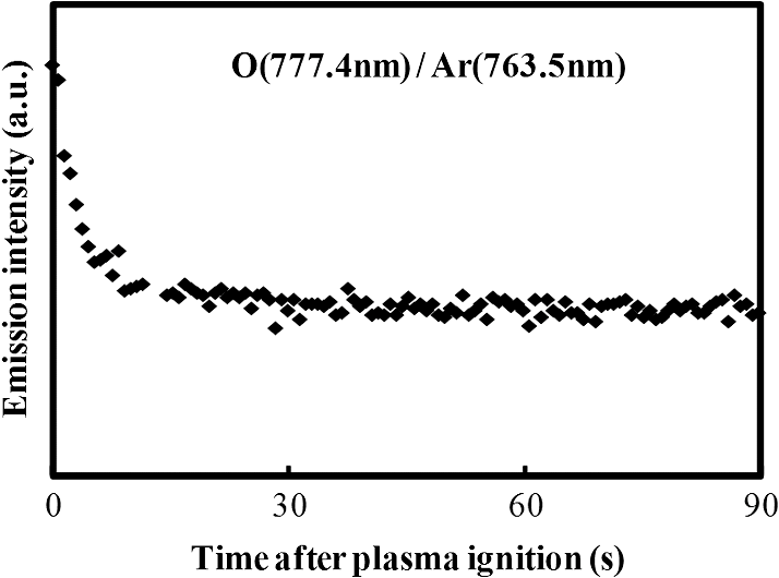 Time dependence of etching depth with IBE was evaluated next. By using IBE, it was possible to avoid the etching-rate change (namely avoid the PMMA-etching-rate enhancement by oxygen impurities), because PMMA is etched only by argon ions when the PMMA and plasma (i.e., ion source) are separated. Furthermore, the etching-rate change due to variations in the ion-source condition can be suppressed by using IBE, because the shutter used in IBE does not open until the ion current reaches a stable value. Time dependences of PMMA etching depth for IBE are shown in Fig. 4. According to the figure, etching depth increases linearly with increasing etching time until it reaches 26.7 nm, and the etching rate is reduced to less than one half of its initial value after the etching depth exceeds 26.7 nm. This result indicates that the change in concentration of oxygen impurities is not the cause of the reduction in etching rate. 3.3.Effect of Surface Oxygen on PMMA EtchingTo identify the cause of the reduction in PMMA etching rate, the surface composition of PMMA was examined by XPS with an argon-ion gun. Oxygen-to-carbon (O/C) ratios are plotted in Fig. 5 as a function of argon-ion irradiation time. Acceleration voltage of the ion gun was either 500 V or 3 kV, while ion current was kept at . The O/C ratios were calculated from the narrow-scan spectra of and . According to the figure, O/C ratio decreases with increasing ion-irradiation time. Moreover, the reduction of O/C ratio is more rapid under high-ion energy conditions (i.e., 3 kV). These results provide strong evidence that the reductions in etching rate for both argon plasmas and IBE are caused by the depletion of oxygen concentration by ion bombardment. This finding is consistent with a previous study, which showed that etching rate of organic materials decreases with decreasing O/C ratio.14 Fig. 5Time dependence of O/C ratio in the PMMA film measured by x-ray photoelectron spectroscopy (XPS) with argon-ion gun. Acceleration voltage of the ion gun was 500 V or 3 kV with constant ion current of . 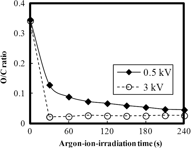 To evaluate the PMMA/PS etching selectivity, the changes in O/C ratio due to argon-ion irradiation in the cases of PMMA and PS were compared (Fig. 6). Acceleration voltage of ion irradiation was 3 kV, ion current was , and irradiation time was 60 s. The O/C ratio of PMMA decreases from 0.35 to 0.026 after ion irradiation. On the other hand, the O/C ratio of PS is almost unchanged (i.e., decreases from 0.059 to 0.057). A small change in PS etching rate is therefore expected, because the change of O/C ratio of PS is much smaller than that of PMMA. The O/C ratio of PS is considered to be zero, because there is no oxygen in PS according to the PS molecular structure in Fig. 1(a). However, the peak of in PS is observed by our XPS analysis, and the O/C ratio of PS does not become zero. The origin of oxygen is tentatively identified as oxygen absorbed during air exposure or oxygen existing as production impurities, such as lubricant or surfactant molecules, in the initial films. The PS film was etched in argon plasma for 300 s at 200-W source power, 5-W bias power, and 2.0-Pa gas pressure. PS etching depth was estimated to be 42.5 nm. On the assumption that PS etching rate is constant regardless of etching depth, high PMMA/PS etching selectivity, namely 6.9, is expected when the depth is below 15 nm. The lower etching rate of PS compared with PMMA is due to the difficulty in breaking the stable benzene ring to form volatile species, as described in Sec. 3.1. Fig. 6Comparison of O/C ratio change by argon-ion irradiation of PMMA and PS. Irradiation conditions: 3-kV acceleration voltage, ion current, and 30-s irradiation time. 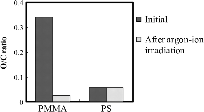 The change in O/C ratio of PMMA is probably due to the change in oxygen composition that comes from the following two origins: One is the oxygen originally contained in the film, as shown in Fig. 1(b) and the other is the oxygen absorbed to the film surface during air exposure. To investigate the oxygen-composition change due to air exposure, the difference in the surface compositions before and after air exposure was evaluated. Two wide-scan spectra taken by XPS are shown in Fig. 7: one was taken immediately after 30-s argon-ion irradiation under 3-kV acceleration voltage and the other was taken after 120-s air exposure after argon-ion irradiation. Clearly, the peak height of increases after air exposure. Furthermore, O/C ratio, which is calculated from the narrow-scan spectra, increases from 0.026 to 0.098 after air exposure. According to these results, it is expected that PMMA etching rate will be increased by air exposure, because the oxygen composition is increased by air exposure. Fig. 7Comparison of wide-scan spectra of PMMA measured by XPS before and after air exposure: (a) wide-scan spectrum after 30-s argon-ion irradiation under 3-kV acceleration voltage and ion current and (b) wide-scan spectrum after 120-s air exposure. 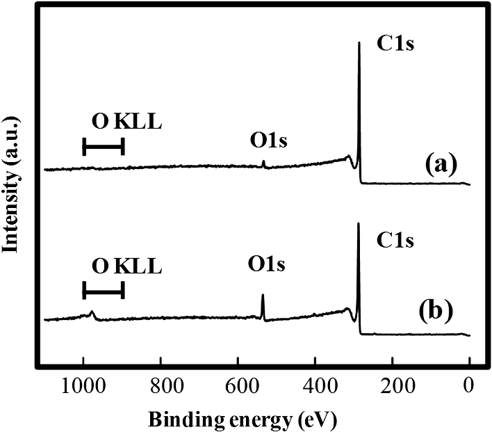 To clarify the effect of air exposure on etching rate of PMMA, the time dependence of etching depth was evaluated. Measured etching depth in an ion-beam etched sample without any treatment before IBE is plotted in Fig. 8. Measured etching depth of an ion-beam etched sample that was etched by argon plasma before IBE is also plotted in the graph. The etching time in the case of the argon plasma was 32 s under 200-W source power, 50-V FSV, 5-W bias power, and 2.0-Pa gas pressure. These two samples were exposed to air for more than 1 day before IBE. Both etching depths show a similar dependence on IBE time. In particular, the slopes of etching depth up to 15 s are much steeper than those after 15 s. This finding suggests that surface-oxygen composition (i.e., O/C ratio) of the sample after 32-s plasma etching is depleted. However, etching depth rapidly increased during the early etching stage, even in the case of the sample with argon-plasma pretreatment. This result shows that the primary cause of etching-rate reduction is attributed not to the reduction in oxygen composition in the film, but to the reduction in oxygen absorbed by the film surface during air exposure. It should be noted that high PMMA/PS etching selectivity when the depth is below 15 nm may be unstable, because the amount of attached oxygen easily changes according to the storage condition. Fig. 8Comparison of time dependence for two PMMA samples: (a) untreated sample before IBE and (b) etched sample by argon plasma before IBE. Etching time of argon plasma was 32 s (which is one of the points plotted in Fig. 2). Sample (b) was exposed to air for about 1 day between plasma etching and IBE. 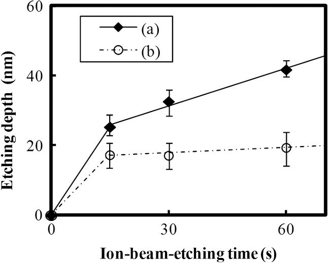 3.4.Effect of Oxygen Addition to Argon PlasmaTo avoid the change in PMMA/PS etching selectivity due to etching-rate change and variable storage conditions, a small amount of oxygen was added to the argon plasma. The time dependences of etching depth for a pure-argon plasma, argon plasma with 1% oxygen addition, and pure oxygen plasma are plotted in Fig. 9. Bias power was 5 W, and gas pressure was 2.0 Pa. In the case of pure oxygen plasma, plasma-source power was adjusted to ensure that the ion energy was the same as that in the case of the argon-based plasma. The samples etched in mixed argon-oxygen plasma and oxygen plasma only show linear dependences of etching depth on etching time, even when the etching depth exceeded 50 nm. This result indicates that the addition of a slight amount of oxygen to the argon plasma suppresses the variation in etching rate due to the depletion of oxygen concentration during plasma etching. The value of PMMA/PS etching selectivity in the case of the mixed argon-oxygen plasma was estimated to be 4.2 at 60-s etching time. Fig. 9Time dependence of PMMA etching depth with the addition of oxygen to argon plasma: (a) argon plasma with 200-W source power, (b) addition of 1% oxygen gas to argon plasma with 200-W source power, and (c) oxygen plasma with 600-W source power. Plasma-etching conditions were 50-V FSV, 5-W bias power, and 2.0-Pa gas pressure in all lines. Source power was controlled so that the time dependences could be compared under the same ion energy.  Etched fingerprint patterns of PS-b-PMMA, which have three kinds of patterns with full pitches, are shown in Fig. 10. The mixed argon-oxygen plasma was used to fabricate these patterns. It is clear from these images that fine PS mask patterns with a full pitch in the range of 25.5 to 77 nm were successfully formed with the mixed argon-oxygen plasma. 4.Concluding RemarksEtching characteristics of argon-oxygen-based plasmas, which are promising for highly selective PMMA etching of PS-b-PMMA, were investigated. Time dependence of etching depth in argon plasma shows that etching rate decreases by more than half after etching to a depth of around 15 nm. The results of XPS analysis of the PMMA surface revealed that the reduction in etching rate is caused by a depletion of oxygen concentration by argon-ion bombardment. To compensate for the decrease in oxygen concentration, 1% oxygen was added to the argon plasma. As a result, PMMA etching rate was constant, even beyond the etching depth of 50 nm. Fine PS mask patterns with full pitches in the range of 25.5 to 77 nm were successfully formed by using the mixed argon-oxygen plasma. It is thus concluded that this mixed argon-oxygen plasma will provide selective PMMA/PS etching for next-generation nanoscale patterning. ReferencesM. P. Stoykovichet al.,
“Directed assembly of block copolymer blends into non-regular device-oriented structures,”
Science, 308
(5727), 1442
–1446
(2005). http://dx.doi.org/10.1126/science.1111041 SCIEAS 0036-8075 Google Scholar
C. J. HawkerT. P. Russell,
“Block copolymer lithography: merging “bottom-up” with “top-down” processes,”
MRS Bull., 30
(12), 952
–966
(2005). http://dx.doi.org/10.1557/mrs2005.249 MRSBEA 0883-7694 Google Scholar
S. Kimet al.,
“Epitaxial self-assembly of block copolymers on lithographically defined nanopatterned substrates,”
Nature, 424
(6947), 411
–414
(2003). http://dx.doi.org/10.1038/nature01775 NATUAS 0028-0836 Google Scholar
C. T. Blacket al.,
“Polymer self-assembly in semiconductor microelectronics,”
IBM J. Res. Dev., 51
(5), 605
–633
(2007). http://dx.doi.org/10.1147/rd.515.0605 IBMJAE 0018-8646 Google Scholar
J. Y. Chenget al.,
“Dense self-assembly on sparse chemical patterns: rectifying and multiplying lithographic patterns using block copolymers,”
Adv. Mater., 20
(16), 3155
–3158
(2008). http://dx.doi.org/10.1002/adma.v20:16 ADVMEW 0935-9648 Google Scholar
L.-W. Changet al.,
“Experimental demonstration of aperiodic patterns of directed self-assembly by block copolymer lithography for random logic circuit layout,”
in IEEE International Electron Devices Meeting (IEDM),
752
–755
(2010). Google Scholar
“The International Technology Roadmap for Semiconductor,”
(2013) http://public.itrs.net/ June ). 2013). Google Scholar
Y. Tadaet al.,
“Directed self-assembly of diblock copolymer thin films on chemically-patterned substrates for defect-free nano-patterning,”
Macromolecules, 41
(23), 9267
–9276
(2008). http://dx.doi.org/10.1021/ma801542y MAMOBX 0024-9297 Google Scholar
L. Oriaet al.,
“Guided self-assembly of block-copolymer for CMOS technology: a comparative study between grapho-epitaxy and surface chemical modification,”
Proc. SPIE, 7970 79700
(2011). http://dx.doi.org/10.1117/12.878486 PSISDG 0277-786X Google Scholar
F. S. BatesG. H. Fredrickson,
“Block copolymer thermodynamics: theory and experiment,”
Annu. Rev. Phys. Chem., 41 525
–527
(1990). http://dx.doi.org/10.1146/annurev.pc.41.100190.002521 ARPLAP 0066-426X Google Scholar
A. K. Khandpuret al.,
“Polyisoprene-polystyren diblock copolymer phase diagram near order-disorder transition,”
Macromolecules, 28
(26), 8796
–8806
(1995). http://dx.doi.org/10.1021/ma00130a012 MAMOBX 0024-9297 Google Scholar
R. B. Fox,
“Glass transition temperature for selected polymers,”
CRC Handbook of Chemistry and Physics, CRC Press, Boca Raton, Florida
(2008). Google Scholar
Y. H. Tinget al.,
“Plasma etch removal of poly(methyl methacrylate) in block copolymer lithography,”
J. Vac. Sci. Technol., B26
(5), 1684
–1689
(2008). http://dx.doi.org/10.1116/1.2966433 JVSTAL 0022-5355 Google Scholar
F. Yamashitaet al.,
“Exploration of suitable dry-etch technologies for direct self-assembly,”
Proc. SPIE, 8328 83280T
(2012). http://dx.doi.org/10.1117/12.916349 PSISDG 0277-786X Google Scholar
T. Chevolleauet al.,
“Self assembly patterning using block copolymer for advanced CMOS technology: optimization of plasma etching process,”
Proc. SPIE, 8328 83280M
(2012). http://dx.doi.org/10.1117/12.916399 PSISDG 0277-786X Google Scholar
K. AsakawaT. Hiraoka,
“Nanopatterning with microdomains of block copolymers using reactive-ion etching selectivity,”
Jpn. J. Appl. Phys., 41
(10), 6112
–6118
(2002). http://dx.doi.org/10.1143/JJAP.41.6112 JJAPA5 0021-4922 Google Scholar
C. C. Liuet al.,
“Pattern transfer using poly(styrene-block-methyl methacrylate) copolymer films and reactive ion etching,”
J. Vac. Sci. Technol., B25
(6), 1963
–1968
(2007). http://dx.doi.org/10.1116/1.2801884 JVSTAL 0022-5355 Google Scholar
R. A. Farrellet al.,
“Monitoring PMMA elimination by reactive ion etching from a lamellar PS-b-PMMA thin film by ex situ TEM methods,”
Macromolecules, 43
(20), 8651
–8655
(2010). http://dx.doi.org/10.1021/ma101827u MAMOBX 0024-9297 Google Scholar
H. GokanS. EshoY. Ohnishi,
“Dry etch resistance of organic materials,”
J. Electrochem. Soc., 130
(1), 143
–146
(1983). http://dx.doi.org/10.1149/1.2119642 JESOAN 0013-4651 Google Scholar
M. Edamuraet al.,
“A novel plasma etching tool with RF-biased faraday-shield technology: chamber surface reaction control in the etching of nonvolatile materials,”
Jpn. J. Appl. Phys., 42
(1), 7547
–7551
(2003). http://dx.doi.org/10.1143/JJAP.42.7547 JJAPA5 0021-4922 Google Scholar
Semiconductor Dry Etching (Hanndoutai Dorai Ecchinngu Gijyutsu), 6th ed.Sanngyou Tosho, Tokyo, Japan
(2004). Google Scholar
Biography Makoto Satake received his BS and MS degrees in applied physics from Tokyo University of Science, Tokyo, Japan, in 2004 and 2006, respectively, where he researched the method of ferroelectric-single-crystal growth. After graduation, he joined Hitachi’s Central Research Laboratory, Tokyo, in 2006, where he did research in plasma etching technique, especially for DSA etching and nonvolatile material etching.  Taku Iwase received his BS and MS degrees in materials science and engineering from Tohoku University, Miyagi, Japan, in 2007 and 2009, respectively, where he developed magnetic resistive device using Heusler alloy. After graduation, he joined Hitachi’s Central Research Laboratory, Tokyo, in 2009, where he did research in the areas of magnetic materials etching and DSA etching.  Masaru Kurihara received his BS, MS, and PhD degrees in electrical engineering from Keio University, Tokyo, Japan, in 1996, 1998, and 2001, respectively, where he developed the plasma simulator, especially for electron swarm and micro-cell plasma. After graduation, he joined Hitachi’s Central Research Laboratory, Tokyo, in 2001, where he did research in the areas of gate etching and metal etching. His main research interests are fab-wide process control and process modeling in a gate-module formation.  Nobuyuki Negishi was awarded his BE and ME degrees in precision engineering from Osaka University in Japan in 1994 and 1996 respectively, where he researched the characteristics of atmospheric pressure plasma. After his graduation, he commenced his career with Central Research Laboratory of Hitachi, Tokyo, in 1996, where he was responsible for development of etching systems and processes for semiconductor manufacturing. His main research area is oxide etching process, especially profile evolution and its mechanisms.  Yasuhiko Tada has been a member of the research staff at Hitachi Research Laboratory, Hitachi Ltd., since 2004. He received his master’s degree in material chemistry and his doctorate degree in polymer chemistry from Kyoto University in 2004 and 2012. His research interests focus on the self-assembled materials and structures of block copolymers for nanofabrication.  Hiroshi Yoshida received a Dr. Eng. degree in polymer chemistry from Kyoto University in 1992. From 1993 to 1998, he joined Hashimoto Polymer Phasing Project, ERATO, Japan Science & Technology Corporation (JST), as a research scientist. In 1998, he moved to Hitachi Research Laboratory, Hitachi Ltd. His current interest includes directed self-assembly processes for next generation nano-scale electronic and biodevice fabrication. He is a member of American Chemical Society. |
|||||||||||||||