|
|
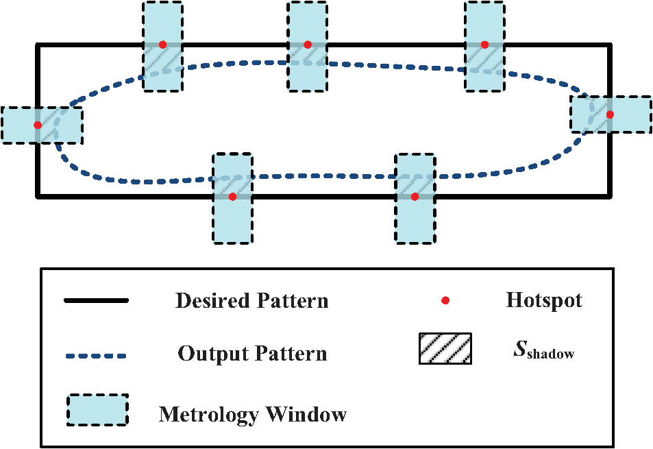
1.IntroductionWith ever-shrinking feature size, the physical characteristics of optics have stronger impacts on the imaging system. In particular, the band-limit system causes the output pattern to be a warped version of the input mask.1 Several resolution enhancement techniques (RETs) have been developed to improve the performance of optical lithography.1–3 Optical proximity correction (OPC) is one of these RETs.4 Its objective is synthesizing an input mask to deliver a desired output pattern. Inverse lithography technique (ILT), as an active approach to OPC, is considered as an economically viable way to meet various challenges in future technology nodes. The computational efficiency of ILT is most noteworthy, especially when handling a large-scale (or full-chip) optimization problem. Generally, ILT treats the mask synthesis as an inverse mathematical problem that aims at minimizing a cost function for the difference between the output and desired patterns. Various computation techniques have been proposed to deal with this inverse problem in the literature, such as the level-set method,5–8 the discrete cosine transform (DCT)-based method,9 and the gradient-based method.10–15 The level-set method treats a mask as a sophisticated continuum,5–8 and consequently, the boundary of the mask is iteratively evolved according to an optimization algorithm. The DCT-based method transforms a mask to the frequency space using a two-dimensional DCT.9 The low frequency components of the mask are adopted, and the corresponding coefficients are iteratively changed in the optimization process. As a result, the synthesized mask only possesses low frequency components and is therefore less complex. The above two techniques can both result in a smooth mask contour, while they are both limited in searching for the whole solution space. The gradient-based method considers a mask as a raster image constituted by pixels directly, where it is synthesized pixel-by-pixel in an iterative direction of the steepest descent, conjugate gradient, and so on.8,10–15 It is probably the most popular technique in the literature due to its high flexibility, ease of understanding, and implementation. Since the mask is discretized into pixels in ILT, such flexibility often causes the synthesized mask to be a gray-level image and it may possess small, unwanted block objects, such as isolated holes, protrusions, and jagged edges, which in turn are unreachable during the real manufacturing.10–15 To address these problems, regularization approaches are introduced to guarantee the synthesized mask to be binary and less complex. In the literature, almost all the regularization approaches take the regularization terms as penalty functions incorporated into a cost function with corresponding weighted parameters10–15 as Here, the operator implements the forward mapping from the input mask to the output pattern, is the desired output pattern, and is the various regularization terms. Generally, regularization terms can be classified into two types: one is related to the manufacturability, such as the quadratic penalty term,11,12 the total variation penalty term,11,12 and the wavelet penalty term;13,15 the other type is related to the fabrication process, such as the image slope term14,16 and the mask error enhancement factor (MEEF).17,18 is the weight of the corresponding regularization term . It should be noted that plays a critical role in the optimization process; however, how and why values of are chosen is rarely discussed in the literature. From experience, it is usually initially set to be a constant.10–15 Here, we take the quadratic penalty term as an example to illustrate how the weighted parameter impacts the optimization process. In this case, both the lower pattern error and the mask quadratic error are preferred, where the pattern error is calculated by and the mask quadratic error is equal to the value of the quadratic penalty term . As shown in Fig. 1, a smaller weighted parameter of this quadratic penalty term results in a rapid convergence on pattern error. It is observed from Fig. 1(a) that the pattern error may meet the requirement after 44 iterations where the mask quadratic error is pretty high at this moment; but it still needs extra iterations to reduce the mask quadratic error. On the other hand, a larger results in good performance on the mask quadratic error while causing poor convergence on the pattern error, as Fig. 1(d) reveals. As shown in Fig. 1, the convergence of the pattern error and the mask quadratic error under such a regularization framework is out of synchronization. Notice that a smaller will not achieve the regularization effects, whereas a larger may result in a larger pattern error; it is, therefore, difficult to choose an appropriate constant value of . Moreover, the choice of has a close relation with the mask features and the simulation resolution. In mathematics, a solid approach is that the is adaptive with each iteration. However, this, in turn, increases the freedom of design variable, and it is generally difficult to accomplish. Fig. 1Convergence of pattern error, mask quadratic error, and cost function values with different weighted parameters of the quadratic penalty term, for the desired pattern in Fig. 11. 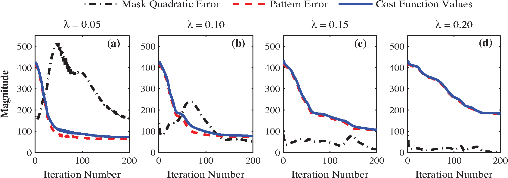 Most recently, we propose an alternative regularization framework that regularizes mask directly by using a mask filtering technique.19 In such a framework, the original cost function Eq. (1) is changed to Eq. (2) as where is a mask filtering operator, the design of which is based on manufacturing constraints. It is noted that the pattern error of the filtered mask instead of the original mask is calculated and will be iteratively reduced in the optimization process. The filtering technique is widely used in signal and image processing and has been used for many years in various application fields as a numerical method to ensure regularity or existence of solutions to an engineering problem, such as structural topology optimization problems.20,21 In this article, gray-level transitions and small, unwanted block objects in the mask are all interpreted as unwanted noise, and it is therefore natural to use filters to remove or prevent this noise in order to satisfy the manufacturing constraints. Section 2.4 details this mask filtering technique.Moreover, we introduce a metric called edge distance error (EDE) to guide mask synthesis in the ILT framework and establish the correlation between pattern error and edge placement error (EPE) via EDE. EPE is popularly used in the polygon-based OPC to convey critical dimension (CD) information, which is essentially the CD error at one side.4 However, it is seldom used in an ILT framework due to its discrete form. One reason is that the gradient (or sensitivity) of EPE with respect to the mask (calculated by a numerical differentiation method) has a computational complexity of , where is the total number of mask pixels in the simulation area and is significantly slower than an analytical gradient calculation with the computational complexity of .10,11 Therefore, pattern error instead of EPE is applied in an ILT framework for its continuous expression and high computational efficiency.6–8,10–15 The pattern error employs an approximated and continuous resist model, and it is defined as a square of the norm of the difference between the output pattern of the input mask and the desired feature, which causes pattern error to be continuous and differentiable with respect to the input mask explicitly.10,11 However, pattern error is a dimensionless quantity and highly depends on mask feature and simulation parameters, such as simulation area and simulation resolution. For this reason, pattern error is not popular in the industry. In this paper, we, therefore, introduce the metric EDE, which has the same dimension as EPE and has a continuous expression as pattern error. The detailed description of EDE will be given in Sec. 2.2. In addition, with the CD decreasing, the printed dimension becomes increasingly sensitive to the fluctuation of the fabrication process, which limits the yield in the semiconductor industry. Instead of using process penalty terms, such as the image slope term and the MEEF, a statistical strategy is applied to minimize a cost function under different process variations weighted by their statistical probability to enhance the robustness of layout patterns.7,22–27 This method is directly related to the fabrication process and is well understood and easily accomplished, while using the process penalty terms can be considered as a roundabout regularization approach and requires deeper understanding of mask topology and the imaging system. The remainder of this paper is organized as follows. Section 2 details the proposed mask filtering technique. Section 3 provides the simulation results to demonstrate the validity and efficiency of the proposed method. Finally, we draw some conclusions in Sec. 4. 2.Methodology2.1.Lithography Imaging ModelIn this section, we review the general lithography imaging model in ILT.10,15 Abstractly, the imaging process for optical lithography is mathematically described as where represents spatial coordinates (), and the operator implements the forward mapping from the input mask to the output pattern . In practice, the in Eq. (3) consists of the projection optics effect and the resist effect.The projection optics effect, namely the optical image in resist , can be modeled as a pupil function with a partially coherent illumination source.28 This is called the partially coherent imaging system,29 which can be approximated by the sum of the coherent systems method,4 the optimal coherent approximation approach,30 or the analytical circle-sampling technique31 as the superposition of several coherent systems Here, is the ’th optical kernel, is the eigenvalue of the ’th kernel with kernels in total, and denotes the two-dimensional convolution. The resist effect can be approximated by a constant threshold resist model using the following logarithmic Sigmoid function:11 with being the steepness of the Sigmoid function and being the threshold. In reality, is equal to the threshold level of the resist.Combining Eqs. (4) and (5), we can write the lithography imaging equation as 2.2.Edge Distance ErrorDue to the low-pass nature of the optical imaging system, is typically a blurred version of . Generally, the norm is employed as a metric to evaluate the difference between the output pattern and the desired pattern as Here, is called pattern error or fidelity error. The only difference between pattern error and fidelity error is that fidelity error uses a Sigmoid function to characterize the resist effect, whereas pattern error uses a step function. The values of fidelity error and pattern error are almost the same since the steepness of the Sigmoid function is large enough. Therefore, in this paper, we would like to call pattern error without distinguishing between them. It is noted that pattern error is a continuous function and hence, the gradient of with respect to the mask can be analytically calculated. However, this metric is not intuitive, for its magnitude is not directly related to the CD error and strongly depends on the mask feature and simulation parameters, such as simulation grid size. In other words, different simulation parameters will result in a different pattern error although with the same pattern. Therefore, we try to derive a metric from pattern error and explicitly relate it to the commonly used EPE in industry. This metric EDE should convey CD information and be independent of the mask feature and simulation parameters. Figure 2(a) depicts the pixel-based representation of a mask pattern and its output pattern on the wafer, where the red dots are discrete sampling elements (pixels) of the patterns, denotes the absolute difference area between the desired pattern contour and the output pattern contour, and is the perimeter of the desired pattern contour. EDE is defined as Fig. 2(a) Pixel-based representation of a mask pattern and its output pattern on the wafer and (b) polygon-based representation of a mask pattern. 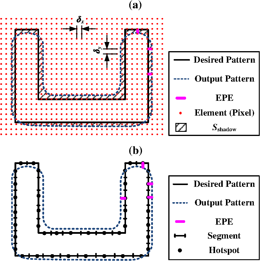 This means that EDE has the dimension of length and thus has an intuitive physical meaning. Assuming the grid size is small enough in Fig. 2(a), the absolute difference area can be approximated by multiplying the total number of elements in shadow and the element area as Here, is the total number of red dots (elements) in shadow, and and are the lengths of the element along the and directions, respectively, as shown in Fig. 2(a). Since the value of the element in the output pattern is either 0 or 1, according to the definition of pattern error in Eq. (7), the number is approximately equal to the pattern error, namely, . So, the absolute difference area can be expressed as Substituting Eq. (10) into Eq. (8), we have the expression of EDE as It is noted that Eq. (11) directly relates EDE to pattern error . The portion of is a constant related to the simulation resolution and desired pattern, which makes pattern error have a dimension of length as EPE. This means that EDE is continuous as pattern error, and the computational complexity of EDE is the same as pattern error, i.e., , where is the total number of elements in shadow as shown in Fig. 2(a). Alternatively, the absolute difference area can be formulated as an integral of EPE taken along the closed desired pattern contour curve : where denotes an infinite small segment on the desired pattern contour curve and is the corresponding segment length. When the pattern contour curve is discretized into a finite number of segments, the pattern is represented as multiple polygons, and this representation is popularly used in polygon-based OPC. In this case, as shown in Fig. 2(b), the absolute difference area can be approximated asHere, is the ’th segment, and is the corresponding length of the segment . Substituting Eq. (13) into Eq. (8), EDE can be alternatively expressed as Therefore, EDE may be interpreted as the mean EPE. Equations (11) and (14) establish the correlation between pattern error and EPE, and these two metrics are actually equivalent in a sense via EDE. Either of the pattern error, EPE or EDE, can act as a metric (or cost function) to guide mask synthesis. However, since EDE has the same dimension as EPE and has a continuous expression as a pattern error, it outperforms the other two. Furthermore, EDE can convey the local CD information and can be weighted by adding some metrology windows. Considering a practical case, customers are sometimes only concerned about some special locations (hotspots) in the resist. In this case, we add a window function around the hotspots as shown in Fig. 3. The value inside the metrology windows is usually set at 1 and that outside at 0. The weighted (or local) area is expressed as Here, is the total number of elements in shadow as shown in Fig. 3 and is approximately equal to the weighted pattern error as where is a window function represented by rectangular functions with appropriate shifting and scaling constants. Hence, the weighted EDE in this case is where is the length of the desired pattern contour within the metrology windows.For simplicity, is used to represent the weighted EDE. Generally, is treated as a cost function to guide mask synthesis under nominal conditions, i.e., no defocus and dosage variations, etc. In order to enhance the process robustness, process variations should be taken into account under the mask synthesizing process. Here, we use the expectation of the weighted EDE under different variations as a cost function as expressed by where denotes the expectation operation over , is a vector representing a combination of multiple process variations including, for example, defocus, exposure dosage variation, and lens aberrations, etc., and is the statistical probability of the corresponding process variations, which is defined by users and is usually obtained via various experiments or measurements of lithographic tools. is called the statistical EDE and is used as a cost function to guide the mask synthesis. The gradient of with respect to mask will be used in the optimization process. According to Refs. (8, 13, and 15), the gradient of with respect to mask is given as where means the conjugate operator; is the steepness of the Sigmoid function in Eq. (5); and is the ’th optical kernel under the process variations ; () is the up–down and left–right flip of .2.3.Inverse Lithography Problem Definition and RegularizationThe objective of inverse lithography is synthesizing an input mask to deliver a desired output pattern. In order to guarantee the manufacturability of synthesized mask, mask quadratic error and complexity should be considered. The quadratic metric and the complexity metric , i.e., total variation, are usually adopted to quantify the corresponding performance. In this paper, we focus on the binary mask. So, the quadratic metric and the complexity metric are expressed, respectively,11,12 as where is the simulation area or the number of pixels in , is the norm, and is an operator of the first derivativeTherefore, combining the optimization objectives of the mask quadratic error, the complexity, and the statistical EDE, we state the inverse lithography problem as It is noted that this problem has three mutually exclusive minimization objectives. In the literature, they are usually combined with certain proportions and to be stated as a single-objective minimization problem:10–15 2.4.Mask Filtering MethodIn this section, we propose an alternative method to solve this multiobjective minimization problem. We first interpret gray-level transitions and small, unwanted block objects, such as isolated holes, protrusions, jagged edges, or other layouts that cannot be fabricated, as unwanted noise in the mask, and then we design a specific filter to remove or prevent this noise to satisfy manufacturing constraints After the filtering process, the quadratic metric and complexity metric of the filtered mask are rather small. Then, we calculate the cost function of this filtered mask Thus, the multiobjective minimization problem is converted into a simpler single-objective minimization problem as We employ an iterative method to solve this problem. In the iteration process, we ensure that the statistical EDE, i.e., , of the filtered mask is iteratively decreasing. It is noted that each obtained mask is filtered and satisfies all the optimization objectives except for the statistical EDE; namely, it satisfies the manufacturing constraints. As a result, we only need to reduce the statistical EDE of this filtered mask. This approach is called the mask filtering technique. The filter operator can be designed based on different mask manufacturing rules. The most basic filter should filter the gray-level image to be a district 0 or 1 and guarantee the mask to be less complex. We, therefore, define a basic mask filter as Here, the steepness of this Sigmoid function is and the threshold is . is a Gaussian filter to relieve mask complexity, where is the center point and means the distance from to . is the normalized weight of the Gaussian filter, where is the number of pixels in . The gradient of with respect to is given asThe detailed derivation of Eq. (28) is given in the Appendix. Combining Eqs. (19) and (28), the gradient of with respect to is With the gradient Eq. (29), we apply a steepest descent method to solve this problem.11 The optimization procedure is
In the above procedure, the iteration is terminated when or or , where is defined as the minimum value of the norm of velocity, is defined as the minimum value of the statistical EDE, and is the prescribed upper limit of the number of iterations. The termination criterion means that the iteration stops when the gradient is zero or rather small. 3.SimulationsSimulations were performed on a partially coherent imaging system with an annular source illumination whose outer radius was and whose inner radius was . The wavelength in the simulations was set at 193 nm, and the numerical aperture (NA) was 1.35. The resist effect was approximated by a Sigmoid function with and . The Gaussian filter consisted of and . The parameters of the Sigmoid function in the proposed filter were and . The parameter and of the initial mask in Eq. (31) were 0.90 and 0.05, respectively; consisted of and . The window function had the same size as the mask image, and all the values were set at 1. Instead of computing the step length in Eq. (38) accurately, we set at a constant 0.3 in each iteration. Since this paper focuses on developing a new regularization framework, process variations will not be taken into consideration in the proposed simulations. That means is the nominal process condition and therefore . All the simulations were carried out with in-house MATLAB codes on a HPZ800 (3.47 GHz Xeon) workstation using a Windows 7 (64 bit) operating system. 3.1.Edge Distance ErrorFigure 4 depicts an example of a desired pattern and its output pattern on the wafer. In this case, the true absolute area between the desired pattern contour and its output pattern contour is , the perimeter of the desired pattern is , and therefore, the true EDE is 10.90 nm. Table 1 summarizes the relative error compared to the true EDE when using different pixel grid sizes. The EDE in Table 1 is calculated by Eq. (11) and the pattern error is calculated by Eq. (7). From Table 1, it is observed that the magnitude of pattern error varies with the pixel grid size, whereas EDE does not. When the pixel grid size is small enough (e.g., 0.5 nm), the EDE calculated by the proposed method is approximately equal to the true EDE. With the increase of pixel grid size, the accuracy of EDE remains acceptable. So, the EDE calculated by the proposed method can be used to guide mask synthesis. Table 1Results of pattern error and edge distance error (EDE) when using different pixel grid sizes.
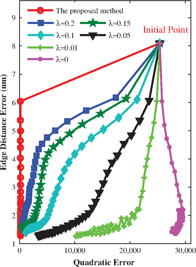
3.2.Mask FilterAs shown in Eq. (25), the proposed mask filter consists of two portions: a Gaussian convolution operation and a Sigmoid (or thresholding) operation. Figure 5 demonstrates these filtering operations, where is a defined Gaussian filter with a size of and , is an intermediate mask pattern with a size of and a grid resolution of 2.5 nm, which is commonly encountered during the optimization process of ILT, and is the filtered pattern calculated by Eq. (25). As expected, the Gaussian convolution operation, , weakens the weight of the small details in , and the Sigmoid operation leads to a sharper contour. As a result, the filtered pattern has a lower complexity, and its mask quadratic error (denoted as QE in Fig. 5) reduces from to 531. Fig. 5Demonstration of the mask filtering operations. is defined as a Gaussian filter, is an intermediate mask pattern, denotes its convolution with the Gaussian filter , represents its filtered pattern, and is the corresponding output pattern on the wafer. The horizontal axis and vertical axis denote position and position of the patterns in nanometers, respectively. 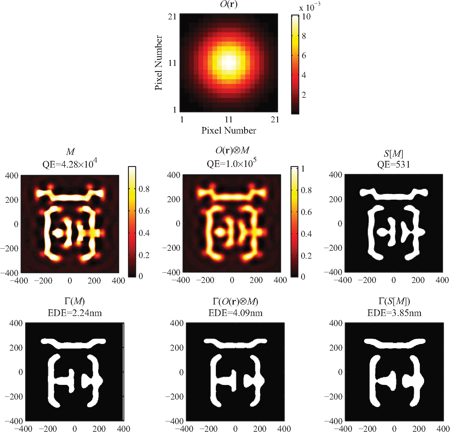 Figure 6 presents another set of simulations for the proposed filter, where is an input mask pattern with a size of and a grid resolution of 2.5 nm. This input mask pattern is artificially introduced with some objects that are difficult to manufacture in practice, including some small isolated holes, protrusions, hollows, and irregular features shown inside the red circles. From the perspective of signal processing, these details can be considered as high-frequency noise in the mask and can be evaluated with total variation.11,12 As revealed in Fig. 6, the total variation (denoted as TV in Fig. 6) of reduces from 3080 to 2416 via the Gaussian convolution operation, which removes these small details. Subsequently, by the Sigmoid operation, it leads to a close-to-binary mask with a total variation of 2677, which reduces total variation by 13.1% compared to the original mask . On the other hand, it is interesting to find that the EDE of the output pattern of the mask , the Gaussian filtered mask, and the filtered mask are almost the same. That is because the optical lithography system with a low-pass nature does not deliver high-frequency details to the output pattern on the wafer. Similar to the optical lithography system, the mask filter acts as a low-pass filter to remove these details that are produced in ILT, whereas it does not cause distortions on the output pattern on the wafer. As demonstrated in Figs. 5 and 6, the proposed filter reduces the mask complexity and achieves a close-to-binary mask, so that the filtered mask is reachable in real manufacture. Fig. 6Performance of the proposed mask filter. is an input mask pattern, denotes its convolution with the Gaussian filter , represents its filtered pattern, and is the corresponding output pattern on the wafer. The horizontal axis and vertical axis denote position and position of the patterns in nanometers, respectively. 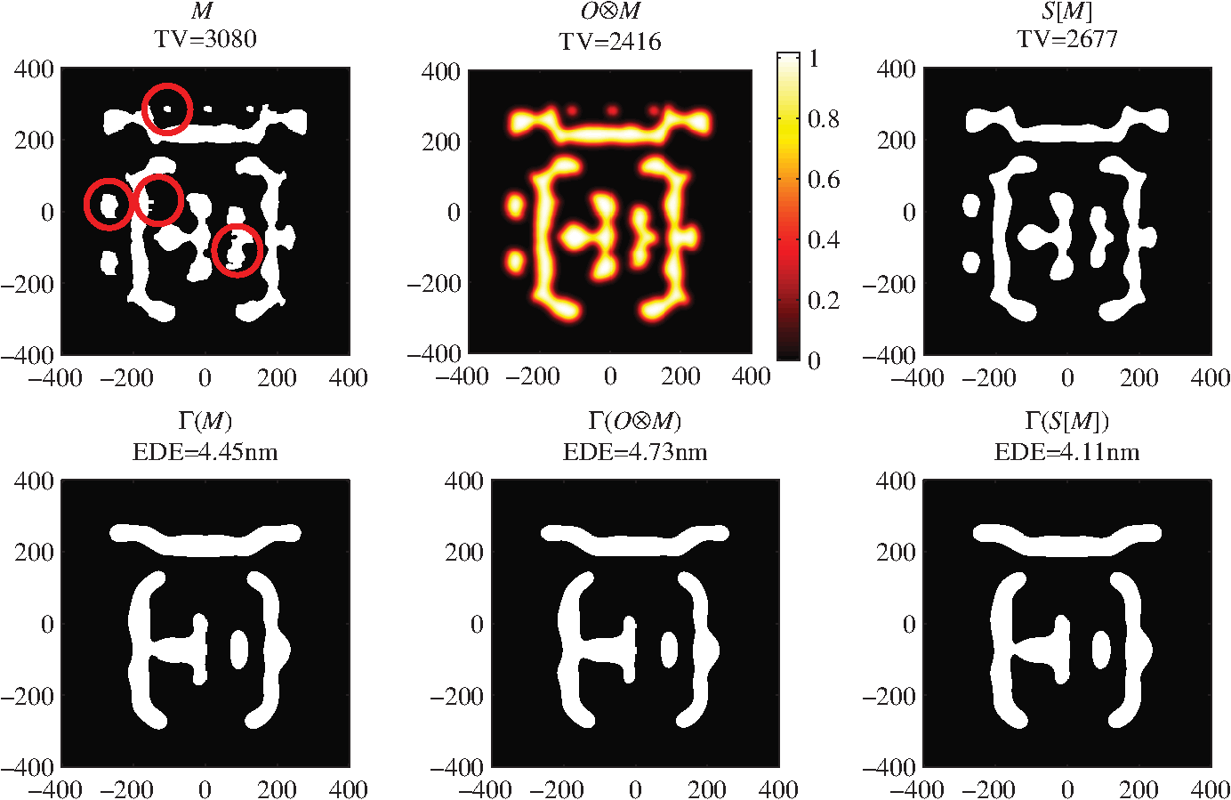 3.3.Results of Mask Filtering TechniqueFigure 7 shows the simulated images by using the proposed method for a desired pattern with a CD of 45 nm. The optimization is terminated after 200 iterations. The desired pattern , which is commonly encountered in the design of static random access memory circuits, consists of with a grid resolution of 2.5 nm. As expected, the optimized mask patterns by the proposed method achieve much smaller EDE compared to that obtained by simply inputting the desire pattern as the mask pattern. It is also observed that the optimized gray-mask is very close to the postprocessing mask and reaches an almost identical output pattern and EDE. This demonstrates that the validity of the proposed method is to synthesize a regular mask pattern and to reach a considerably low EDE. Fig. 7Simulation results for the desired pattern by the proposed method. is the optimized mask, is the binary mask by postprocessing of with a global threshold 0.5, represents the corresponding optical image, and is the output pattern on the wafer. The horizontal axis and vertical axis denote position and position of the patterns in nanometers, respectively. 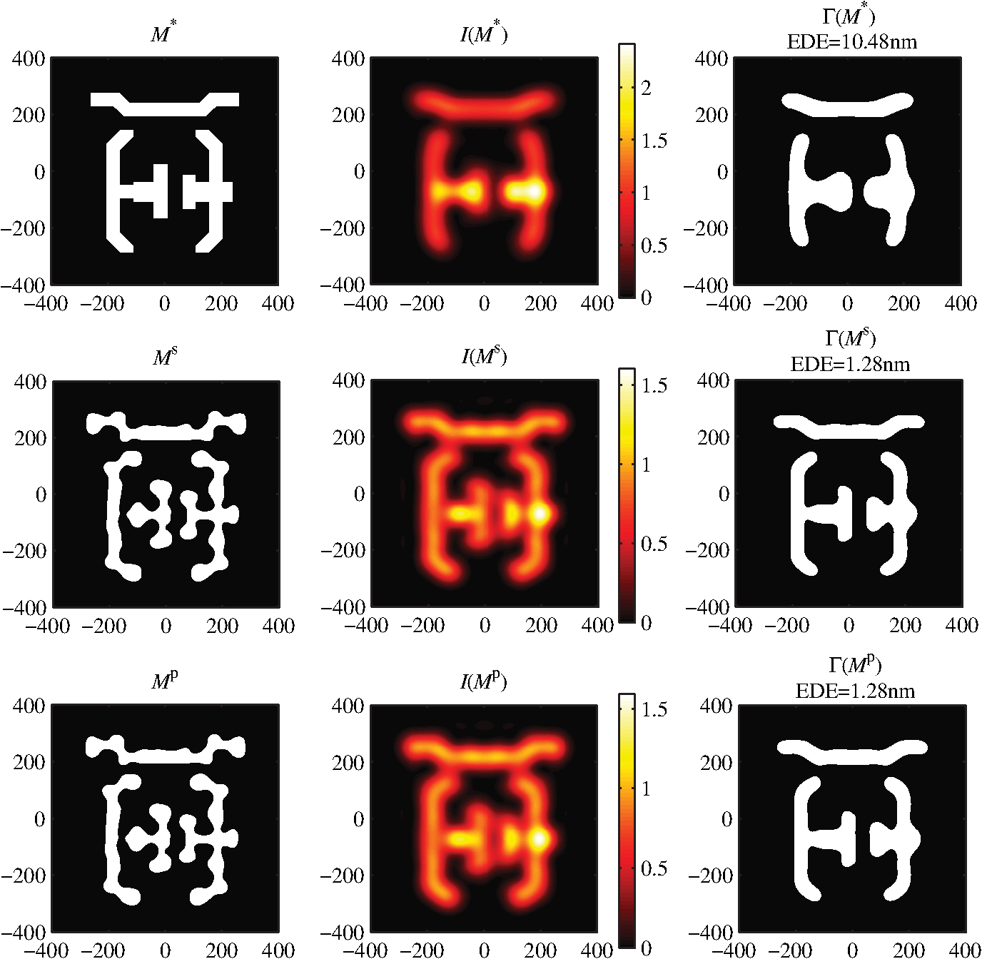 Figure 8 presents some intermediate results obtained in the iteration process by the proposed method. denotes the initial mask and is calculated by using Eq. (31); means the mask that is obtained after the ’th iteration and is calculated by using Eq. (41). The EDE means EDE between the output pattern of the and the desired pattern. It is noted that each obtained intermediate mask by the proposed method is very close to binary and has a low mask complexity. This demonstrates that the proposed method can filter (regularize) the mask to eliminate the gray-level transitions and small, unwanted objects. In comparison, Fig. 9 also shows some intermediate results obtained in the iteration process by the conventional regularization method. The conventional regularization method takes different penalty terms and incorporates them into the cost function with the corresponding weight and then seeks the minimum of such a weighted cost function. In this case, we take the quadratic term, for example, and the corresponding weighted parameter is set at 0.1. From Fig. 9, it is observed that the intermediate result with this method possesses gray-level transitions. The EDE may satisfy a 5% CD error after 50 iterations, while the mask quadratic error is pretty high at this moment; it still needs extra iterations to reduce the mask quadratic error although the EDE achieves the demanded result. This is one of the drawbacks of the conventional regularization method. Comparing Fig. 8 to Fig. 9, the intermediate mask by using the proposed method has a lower level in both mask quadratic error and mask complexity, which is quite an improvement over the conventional regularization method. Since the convergence of EDE and mask quadratic error by the conventional regularization method is out of synchronization, it, therefore, needs several iterations to achieve a low level on both EDE and mask quadratic error, although in the proposed method, the iteration (optimizing process) can be stopped whenever EDE reaches the demanded result without worrying about the manufacturability. Fig. 8Some intermediate results obtained in the iteration process by the proposed method. The horizontal axis and vertical axis denote position and position of the patterns in nanometers, respectively. 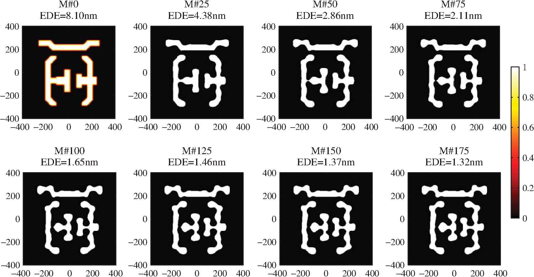 Fig. 9Some intermediate results obtained in the iteration process by the conventional regularization method. The horizontal axis and vertical axis denote position and position of the patterns in nanometers, respectively. 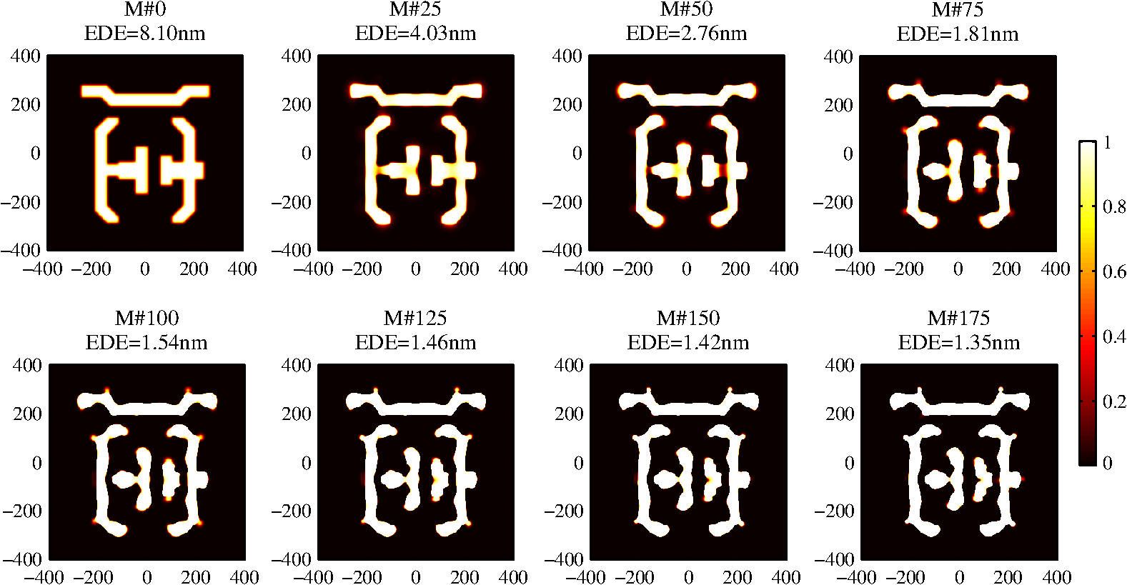 Figure 10 depicts the convergence properties with different methods. The results by the conventional regularization method with different weighted parameters demonstrate that a small weight causes a fast convergence on EDE but results in a slow convergence on mask quadratic error; a large weight results in a fast convergence on mask quadratic error while finally causing a higher EDE. That means a smaller will not achieve the regularization effects, whereas a larger may result in a large EDE. For this reason, it is difficult to choose an appropriate value of weighted parameter to get a win–win situation. This is the second drawback of the conventional regularization method. On the other hand, it is observed that the EDE by the proposed method converges rapidly while the mask quadratic error remains at a low level, which demonstrates that all the intermediate masks satisfy the mask quadratic error constrains. Another two sets of simulations under different illumination conditions are shown in Fig. 11. Simulation of the designed mask pattern is performed on a partially coherent imaging system with an annular source illumination () and the NA of 0.85. The mask , i.e., obtained by the proposed method consists of a size with a grid resolution of 2.5 nm. Simulation of the designed mask pattern is performed on a partially coherent imaging system with a quasar source illumination () and the NA is of 1.25. The mask , i.e., obtained by the proposed method consists of a size with a grid resolution of 2.5 nm. From Fig. 11, it is demonstrated that the proposed method can synthesize a mask pattern under different imaging conditions and shows the possibility of reaching a considerably low EDE. Fig. 11Simulation results for the desired patterns and by the proposed method. and are the optimized masks, and represents the corresponding output pattern on the wafer. The horizontal axis and vertical axis denote position and position of the patterns in nanometers, respectively. 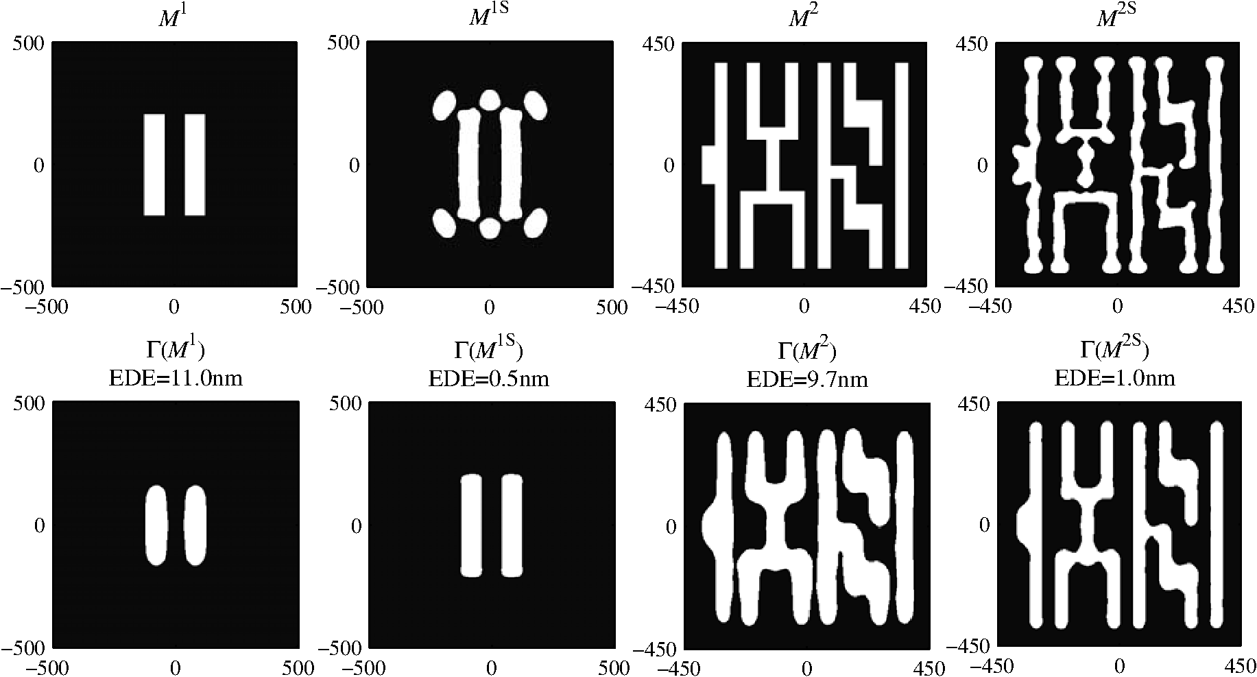 We also performed simulations for more complicated patterns by using the proposed method. Figure 12 depicts the results for one desired pattern , which is a contact layer of the benchmark AND-OR-INVERT gate circuit layout,32 consisting of with a grid resolution of 2.5 nm, i.e., the simulation area is . The proposed method results in a smooth mask pattern with an EDE of 2.11 nm compared to 8.37 nm by simply inputting the desired pattern as the mask pattern. These results further demonstrate that the proposed method has the capability of achieving a small EDE and of ensuring the regularity of the synthesized mask. Fig. 12Simulation results for the desired pattern by the proposed method. is the optimized mask, represents the corresponding optical image, and is the output pattern on the wafer. The horizontal axis and vertical axis denote position and position of the patterns in nanometers, respectively. 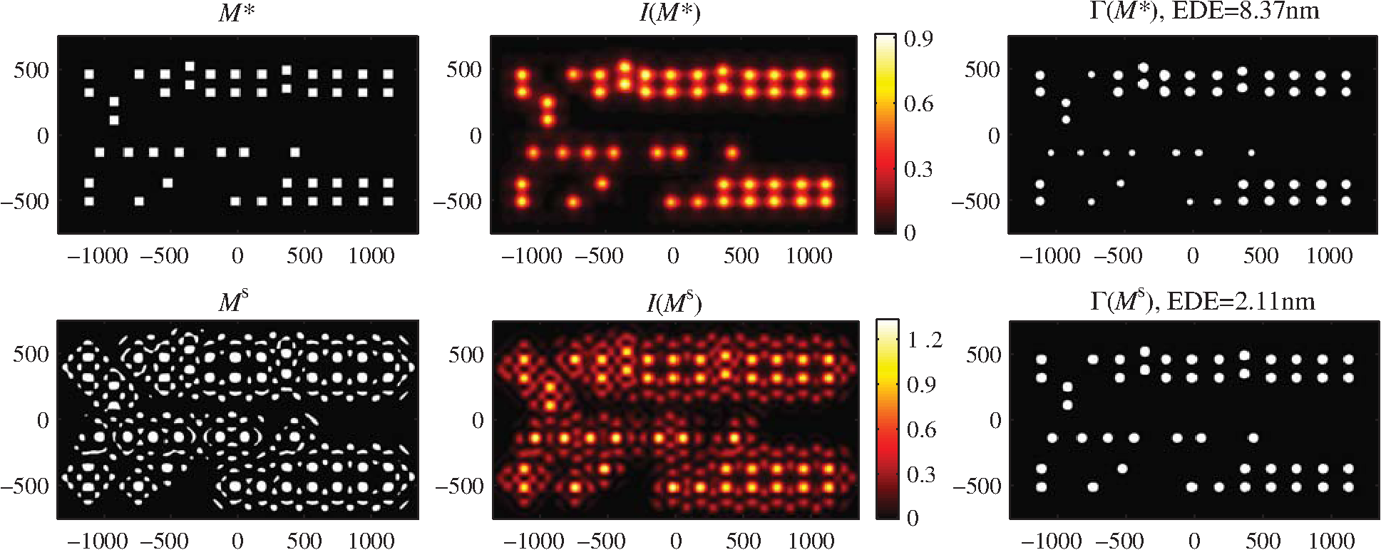 Table 2 summarizes the average runtime of each iteration using different methods with different mask patterns. As revealed in Table 2, the average runtime of each iteration by the proposed method is almost the same as that by the conventional method. That is because the proposed method just adds a computation of Eq. (28), whose runtime is far less than the total calculation time compared to the conventional regularization method. In other words, the proposed method enhances the mask manufacturability with an almost equal runtime. In this perspective, the proposed method is therefore more efficient than the conventional regularization method. Table 2The average runtime of each iteration by different methods with different mask patterns. 4.ConclusionsIn this paper, we have demonstrated the application of a mask filtering technique and the metric EDE to solve the inverse lithography problem. The mask filtering technique interprets gray-level transitions and small, unwanted block objects as unwanted noise in the mask, and employs a filter to remove this noise to satisfy manufacturing constraints. The proposed filter consists of two portions: a Gaussian convolution operation to weaken the weight of the small details in mask and a thresholding operation to produce a sharper contour. The advantage of this approach lies in that it enhances the manufacturability of each intermediate mask without raising computational complexity and avoids choosing weighted parameters of various regularization terms. In addition, we introduce a metric called EDE to guide mask synthesis and establish the correlation between pattern error and EPE. EDE is defined as the absolute area between the desired pattern contour and its output pattern contour divided by the perimeter of the desired pattern. It can be interpreted as the mean EPE and can be approximated by pattern error multiplied by a constant portion that only depends on the simulation resolution and desired pattern. Therefore, EDE has the same dimension as EPE and has a continuous expression as pattern error. The mask filtering technique and the metric EDE are expected to have direct applications in mask optimization and synthesis for optical lithography in semiconductor industry. AppendicesAppendix:Derivation of Eq. (28)To derive Eq. (28), we first give some useful intermediate results such as and where , , and denote the spatial coordinates (). Noticing that is the number of pixels in and is the steepness of the Sigmoid function in , finally we define and derive the gradient of the mask filter with respect to asAcknowledgmentsThis work was funded by the National Natural Science Foundation of China (Grant No. 91023032, 51005091, 51121002), the Specialized Research Fund for the Doctoral Program of Higher Education of China (Grant No. 20120142110019), the National Science and Technology Major Project of China (Grant No. 2012ZX02701001), and the National Instrument Development Specific Project of China (Grant No. 2011YQ160002). ReferencesA. K. Wong, Resolution Enhancement Techniques in Optical Lithography, SPIE Press, Bellingham, Washington
(2001). Google Scholar
L. W. Liebmannet al.,
“TCAD development for lithography resolution enhancement,”
IBM J. Res. Dev., 45
(5), 651
–665
(2001). http://dx.doi.org/10.1147/rd.455.0651 IBMJAE 0018-8646 Google Scholar
F. Schellenberg,
“Resolution enhancement technology: the past, the present, and extensions for the future,”
Proc. SPIE, 5377 1
–20
(2004). http://dx.doi.org/10.1117/12.548923 PSISDG 0277-786X Google Scholar
N. B. Cobb,
“Fast optical and process proximity correction algorithms for integrated circuit manufacturing,”
University of California at Berkeley,
(1998). Google Scholar
L. PangY. LiuD. Abrams,
“Inverse lithography technology (ILT): a natural solution for model-based SRAF at 45 nm and 32 nm,”
Proc. SPIE, 6607 660739
(2007). http://dx.doi.org/10.1117/12.729028 PSISDG 0277-786X Google Scholar
Y. ShenN. WongE. Y. Lam,
“Level-set-based inverse lithography for photomask synthesis,”
Opt. Express, 17
(26), 23690
–23701
(2009). http://dx.doi.org/10.1364/OE.17.023690 OPEXFF 1094-4087 Google Scholar
Y. Shenet al.,
“Robust level-set-based inverse lithography,”
Opt. Express, 19
(6), 5511
–5521
(2011). http://dx.doi.org/10.1364/OE.19.005511 OPEXFF 1094-4087 Google Scholar
W. Lvet al.,
“Level-set-based inverse lithography for mask synthesis using the conjugate gradient and an optimal time step,”
J. Vac. Sci. Technol., B 31
(4), 041605
(2013). http://dx.doi.org/10.1116/1.4813781 JVTBD9 0734-211X Google Scholar
S. ShenP. YuD. Z. Pan,
“Enhanced DCT2-based inverse mask synthesis with initial SRAF insertion,”
Proc. SPIE, 7122 712241
(2008). http://dx.doi.org/10.1117/12.801409 PSISDG 0277-786X Google Scholar
Y. Granik,
“Fast pixel-based mask optimization for inverse lithography,”
J. Micro/Nanolith. MEMS MOEMS, 5
(4), 043002
(2006). http://dx.doi.org/10.1117/1.2399537 JMMMGF 1932-5134 Google Scholar
A. PoonawalaP. Milanfar,
“Mask design for optical microlithography – An inverse imaging problem,”
IEEE Trans. Image Process., 16
(3), 774
–788
(2007). http://dx.doi.org/10.1109/TIP.2006.891332 IIPRE4 1057-7149 Google Scholar
A. PoonawalaP. Milanfar,
“A pixel-based regularization approach to inverse lithography,”
Microelectron. Eng., 84
(12), 2837
–2852
(2007). http://dx.doi.org/10.1016/j.mee.2007.02.005 MIENEF 0167-9317 Google Scholar
X. MaG. R. Arce,
“Binary mask optimization for inverse lithography with partially coherent illumination,”
J. Opt. Soc. Am. A, 25
(12), 2960
–2970
(2008). http://dx.doi.org/10.1364/JOSAA.25.002960 JOAOD6 0740-3232 Google Scholar
J. C. YuP. Yu,
“Impacts of cost functions on inverse lithography patterning,”
Opt. Express, 18
(22), 23331
–23342
(2010). http://dx.doi.org/10.1364/OE.18.023331 OPEXFF 1094-4087 Google Scholar
X. MaG. R. Arce,
“Pixel-based OPC optimization based on conjugate gradients,”
Opt. Express, 19
(3), 2165
–2180
(2011). http://dx.doi.org/10.1364/OE.19.002165 OPEXFF 1094-4087 Google Scholar
N. B. CobbY. Granik,
“Using OPC to optimize for image slope and improve process window,”
Proc. SPIE, 5130 838
–846
(2003). http://dx.doi.org/10.1117/12.504379 PSISDG 0277-786X Google Scholar
N. B. CobbY. Granik,
“Model-based OPC using the MEEF matrix,”
Proc. SPIE, 4889 1281
–1292
(2002). http://dx.doi.org/10.1117/12.467435 PSISDG 0277-786X Google Scholar
Y. Granik,
“Generalized mask error enhancement factor theory,”
J. Micro/Nanolith. MEMS MOEMS, 4
(2), 023001
(2005). http://dx.doi.org/10.1117/1.1898066 JMMMGF 1932-5134 Google Scholar
W. LvQ. XiaS. Y. Liu,
“Pixel-based inverse lithography using a mask filtering technique,”
Proc. SPIE, 8683 868325
(2013). http://dx.doi.org/10.1117/12.2011469 PSISDG 0277-786X Google Scholar
B. Bourdin,
“Filters in topology optimization,”
Int. J. Numer. Methods Eng., 50
(9), 2143
–2158
(2001). http://dx.doi.org/10.1002/(ISSN)1097-0207 IJNMBH 0029-5981 Google Scholar
M. P. BendsøeO. Sigmund, Topology Optimization: Theory, Methods and Application, Springer, Berlin
(2003). Google Scholar
P. YuS. X. ShiD. Z. Pan,
“True process variation aware optical proximity correction with variational lithography modeling and model calibration,”
J. Micro/Nanolith. MEMS MOEMS, 6
(3), 031004
(2007). http://dx.doi.org/10.1117/1.2752814 JMMMGF 1932-5134 Google Scholar
N. JiaE. Y. Lam,
“Machine learning for inverse lithography: using stochastic gradient descent for robust photomask synthesis,”
J. Opt., 12
(4), 045601
(2010). http://dx.doi.org/10.1088/2040-8978/12/4/045601 JOOPDB 0150-536X Google Scholar
N. JiaE. Y. Lam,
“Pixelated source mask optimization for process robustness in optical lithography,”
Opt. Express, 19
(20), 19384
–19398
(2011). http://dx.doi.org/10.1364/OE.19.019384 OPEXFF 1094-4087 Google Scholar
S. Choyet al.,
“A robust computational algorithm for inverse photomask synthesis in optical projection lithography,”
SIAM J. Imaging Sci., 5
(2), 625
–651
(2012). http://dx.doi.org/10.1137/110830356 1936-4954 Google Scholar
S. LiX. WangY. Bu,
“Robust pixel-based source and mask optimization for inverse lithography,”
Opt. Laser Technol., 45 285
–293
(2013). http://dx.doi.org/10.1016/j.optlastec.2012.06.033 OLTCAS 0030-3992 Google Scholar
S. Y. Liuet al.,
“Convolution-variation separation method for efficient modeling of optical lithography,”
Opt. Lett., 38
(13), 2168
–2170
(2013). http://dx.doi.org/10.1364/OL.38.002168 OPLEDP 0146-9592 Google Scholar
A. K. Wong, Optical Imaging in Projection Microlithography, SPIE Press, Bellingham, WA
(2005). Google Scholar
H. H. Hopkins,
“On the diffraction theory of optical images,”
Proc. R. Soc. A, 217 408
–432
(1953). http://dx.doi.org/10.1098/rspa.1953.0071 PRLAAZ 0080-4630 Google Scholar
Y. C. PatiT. Kailath,
“Phase-shifting masks for microlithography: automated design and mask requirements,”
J. Opt. Soc. Am. A, 11
(9), 2438
–2452
(1994). http://dx.doi.org/10.1364/JOSAA.11.002438 JOAOD6 0740-3232 Google Scholar
P. Gonget al.,
“Fast aerial image simulations for partially coherent systems by transmission cross coefficient decomposition with analytical kernels,”
J. Vac. Sci. Technol., B 30
(6), 06FG03
(2012). http://dx.doi.org/10.1116/1.4767442 JVTBD9 0734-211X Google Scholar
The NanGate 45 nm Open Cell Library, v1.3,
(2013) http://www.si2.org/openeda.si2.org/projects/nangatelib July ). 2013). Google Scholar
Biography Wen Lv is currently a PhD candidate at Huazhong University of Science and Technology under the guidance of Prof. Shiyuan Liu. He received his BS degree from the School of Mechanical Science and Engineering of the same university in 2011. His research involves various issues in optical lithography, including inverse lithography, fast optical image simulation, and mask writing technique. He is a student member of SPIE and IEEE.  Qi Xia is an associate professor of the School of Mechanical Science and Engineering at the Huazhong University of Science and Technology, China. He received his PhD degree in mechanical engineering from the Chinese University of Hong Kong (CUHK), China, in 2007. His current interests include structural and material design optimization for microelectromechanical sensors and actuators, mechatronics and automation. He is a member of IEEE.  Shiyuan Liu is a professor of mechanical engineering at Huazhong University of Science and Technology, leading his Nanoscale and Optical Metrology Group with research interest in metrology and instrumentation for nanomanufacturing. He also actively works in the area of optical lithography, including partially coherent imaging theory, wavefront aberration metrology, optical proximity correction, source mask optimization, and inverse lithography technology. He received his PhD in mechanical engineering from Huazhong University of Science and Technology in 1998. He is a member of SPIE, OSA, AVS, IEEE, and Chinese Society of Micro/Nano Technology (CSMNT). He holds 30 patents and has authored or coauthored more than 100 technical papers. |