|
|
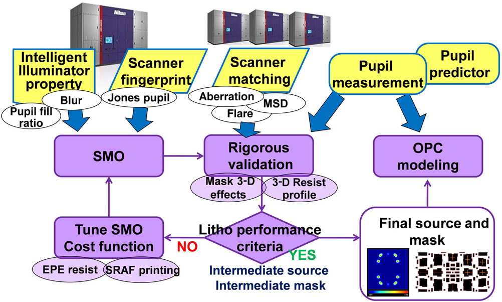
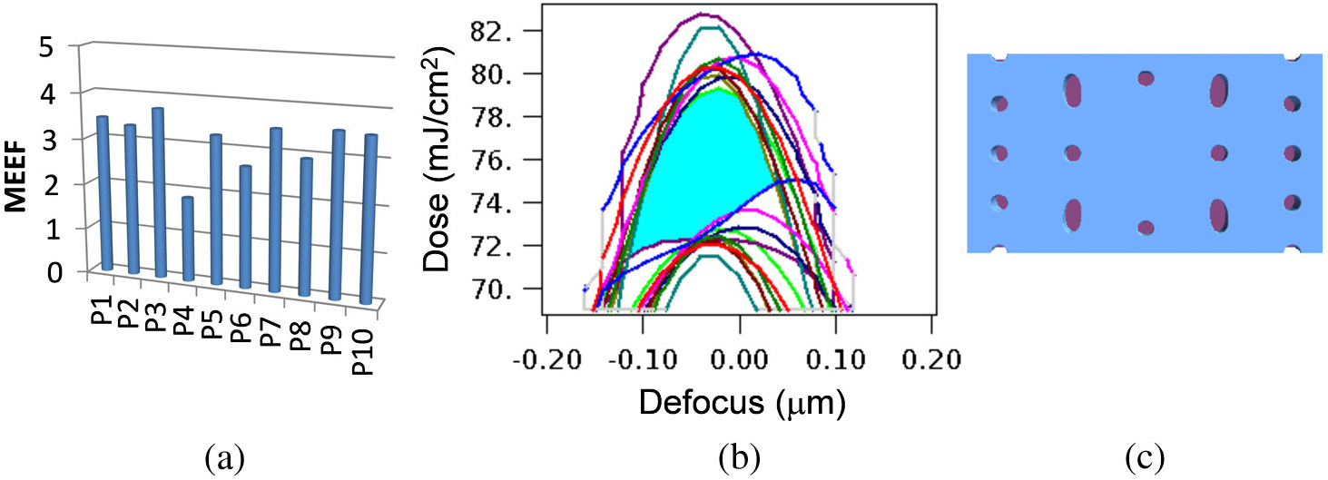
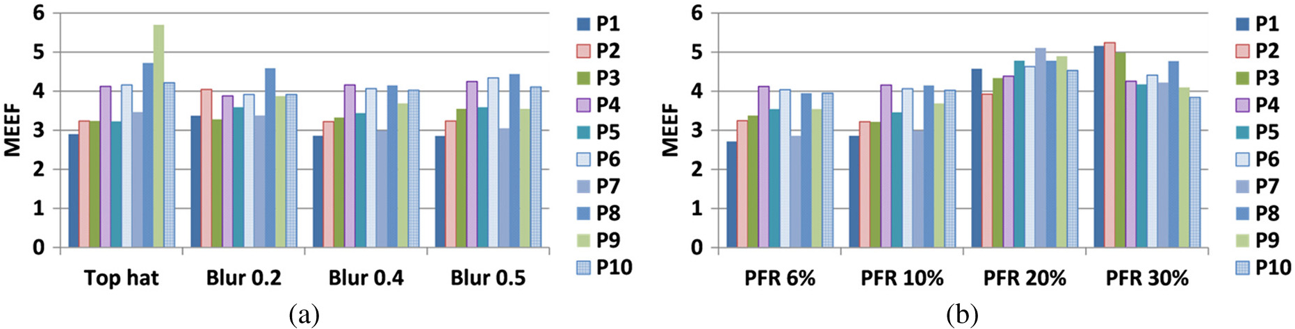
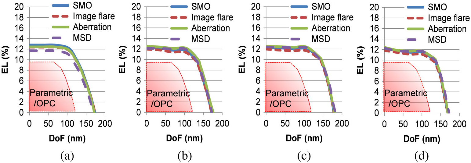
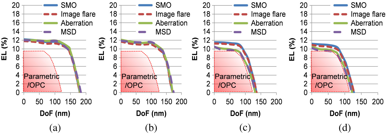
1.IntroductionSource mask optimization (SMO) is being utilized for advanced semiconductor devices below 28-nm node in low k1 immersion lithography in order to obtain a sufficient process window (PW). Many requirements, which were simultaneous co-optimization methodology of source and mask,1 effective source with grid point shape,2 grid mask pattern with manufacturability,3 and the source generation on scanner,4 for proper operation of SMO, had been evaluated. Since lithographers are trying to lower with particular techniques of double patterning and directed self-assembly for pitch shrinking without a shorter wavelength or a higher numerical aperture, a mature SMO solution with high controllability of scanner source and accurate prediction of wafer printing is required. We have developed the Intelligent Illuminator, which is a part of the illumination system on the NSR-S621D scanner, with many degrees of adjustment freedom of intensity distribution in source images. It can provide control of optical proximity effect (OPE) matching between different exposure tools with pupilgram modulation and OPE matching software called “OPE-Master.”5,6 An OPE accuracy of 0.7-nm root mean square (RMS) and an ability of actual source prediction from SMO source with software called “Pupil Predictor”7 meets the SMO demands. Since the actual illuminator has some source constraints of an exclusion zone, a maximum sigma and a minimum pupil-fill ratio (PFR) and properties of intensity blur of the grid point source, the SMO engine should be able to take these parameters into account in optimization for more practical solutions. Proteus SMO,8 which provides a new method of simultaneous SMO allowing a balance of the mask enhancement error factor (MEEF) and depth of focus (DOF) requirements with a flexible cost function and a consideration of mask rule compliance within usable turn around, can use these constraints. In addition, Sentaurus Lithography (S-Litho) can simulate aerial images with a rigorous calculation of electromagnetic field on a thick mask, called the mask three-dimensional (3-D) effect, and a resist profile with the rigorous resist model. By coupling of Proteus SMO and S-Litho, a practical SMO solution with accurate wafer printing without any subresolution assist feature (SRAF) printing can be achievable. When calculating this kind of solution, one must remember that a scanner may have some slight errors in source making in an illumination unit even though it has superior critical dimension (CD) controllability around 1 nm of RMS with the high degree of pupilgram freedom. Errors from aberrations and stray light in projection optics, and a relative stage vibration between reticle stage and wafer stage, also affect imaging quality loss, which must be considered in high volume manufacturing with one source of SMO due to applying multiple scanners. SMO must include scanner variations of the source making. In this paper, we confirm a solution against issues mentioned above with a procedure as shown in Fig. 1. In Sec. 2 of this paper, SMO with typical source properties, a scanner fingerprint, and validation of a rigorous model will be demonstrated. Section 3 shows SMO results of dependency of the properties and an impact of scanner variations. Section 4 will investigate generated sources in Intelligent Illuminator on the various source properties and the scanner variations. 2.Standard Flow of SMOA static-random access memory (SRAM) for a generic 22-nm node with a cell size of on a contact layer (see in Ref. 8) was used for the evaluation. Since, a minimum pitch of the SRAM was 81.2 nm, exposure pattern was divided into two parts for double patterning to relax the pitch to 110 nm as shown in Fig. 2. An NEGA-process,9 which used a negative-tone resist of 100-nm thick on bottom-ARC with 92-nm thick expanding PW in this kind of contact pattern with tighter pitch, was applied. A first iteration of SMO was carried out with a thin-mask model (Kirchhoff), an aerial image base, properties of Intelligent Illuminator and scanner fingerprint of Jones pupil of NSR-621D as Nikon scanner signature file,10 and the target pattern. During this aerial image based SMO run, an edge placement error (EPE) based optimization metric was determined by the intensity contours at fixed -position inside the resist bulk, here 16.5 nm above the resist bottom. Figures 3(a) and 3(b) show SMO result of contour on drawn and corrected patterns with SRAF, MEEF. An MEEF value less than a target value of 4 was obtained. PW-tree, which consisted of an acceptable area of DOF and exposure latitude (EL), was calculated from a common PW as shown in Fig. 3(c). To ensure the effectiveness of the co-optimization, a PW-tree with a quadrupole source and an optimum optical proximity correction (OPC) as the same algorithm of SRAF insertion on SMO was compared as shown in Fig. 4. Over 100 nm of DOF at 6% EL, whose values were PW target value, was obtained and an area of common PW was improved up to 48%. Fig. 2(a) Design intent for static-random access memory (SRAM) cell. The masks for the first and the second exposure steps are marked with different colors. (b) Periodic cell of the first exposure mask, which is being used in the SMO process. 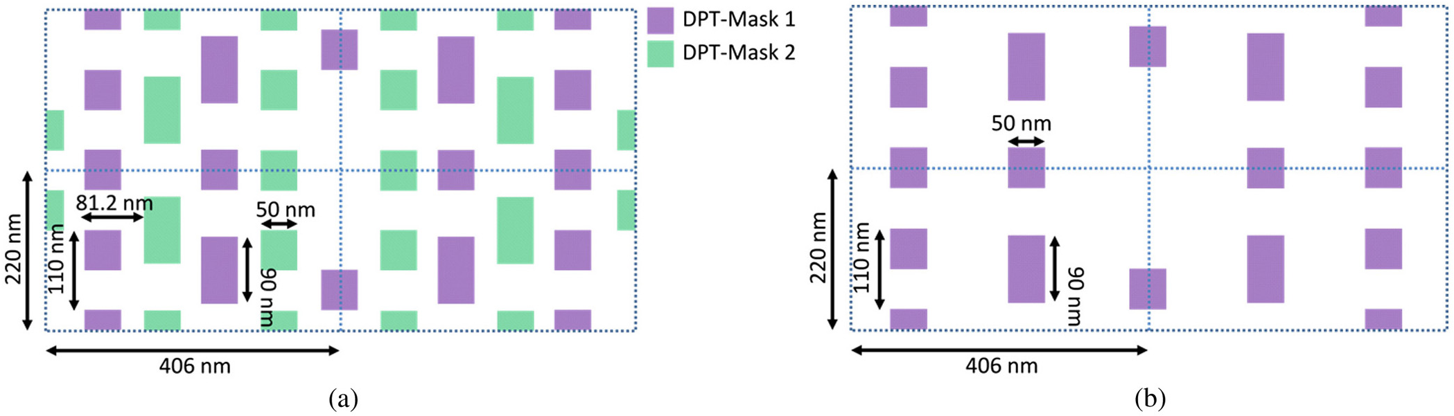 Fig. 3First iteration results of (a) intensity contour and corrected mask pattern with subresolution assist feature (SRAF), (b) mask enhancement error factor (MEEF), and (c) common process window (PW). 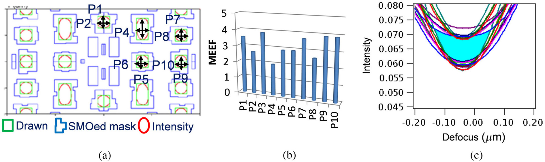 Fig. 4(a) Source shapes of parametric of quadrapole on optical proximity correction (OPC) use and SMO and (b) PW tree of OPC and SMO. 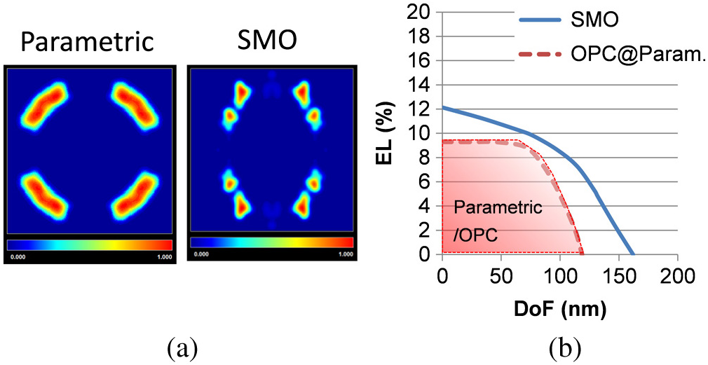 After the first optimization iteration, a validation of the obtained layout and source was performed by including 3-D mask effects in the PW analysis. S-Litho with a waveguide algorithm was used to rigorously simulate the 3-D mask stack of 90-nm thick of Cr. The final result was obtained by interpolating the rigorous results for nine incident angles, closely mapping the illumination source shape. As shown in Fig. 5(a), a strong degradation of the common PW is observed as well as a focus shift and an optimum intensity shift. Furthermore, the optimized layout and source were evaluated in resist, again using S-Litho and a calibrated resist model (see in Ref. 8). Figure 5(b) shows that no usable common PW could be obtained anymore. Furthermore, SRAF printing was observed in the rigorous simulation [Fig. 5(c)]. This clearly shows that an optimization incorporating 3-D mask and resist effects is required. Fig. 5PWs with (a) rigorous 3-D mask simulation and (b) resist simulation and its resist profile of top view. The red dashed line (c) was an area of no target pattern. 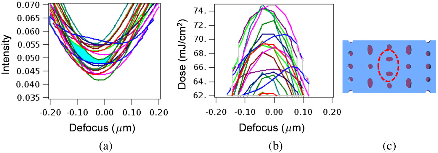 So we performed a mask-only optimization, but employed the effects of mask 3-D and resist property. In the resist based calculation, the optimization metric for EPEs through process variation was changed from EPEs based on intensity contour at a fixed -position to resist profile based EPEs. Figure 6 shows results of validation after final optimization. MEEF was satisfied below 4, which was our specification on all gauges, a common PW was obtained, and SRAFs did not print successfully. 3.Impact of Source Constraints3.1.SMO with Various ConstraintsTo evaluate the effects of source constraints on SMO, an aerial image based SMO was carried out with various source properties of blur and PFR. The blur was a normalized value of Gaussian convolution with a grid point source and the PFR was the ratio of summation of intensity in a pupil to the whole area of the pupil. A 6% of PFR value was used in the blur dependency evaluation and a 0.4 of blur one was used in PFR dependency. Figures 7 and 8 show the results of SMO runs. Common PWs were obtained in all cases of the optimization (see in colored area on PW). Fig. 7SMO results of various blurs of (a) top hat, (b) 0.2, (c) 0.4, and (d) 0.5. In each column, the upper row is the source shape, the middle one is the OPC pattern and SRAF insertion, and the lower one is the common PW with SMO. 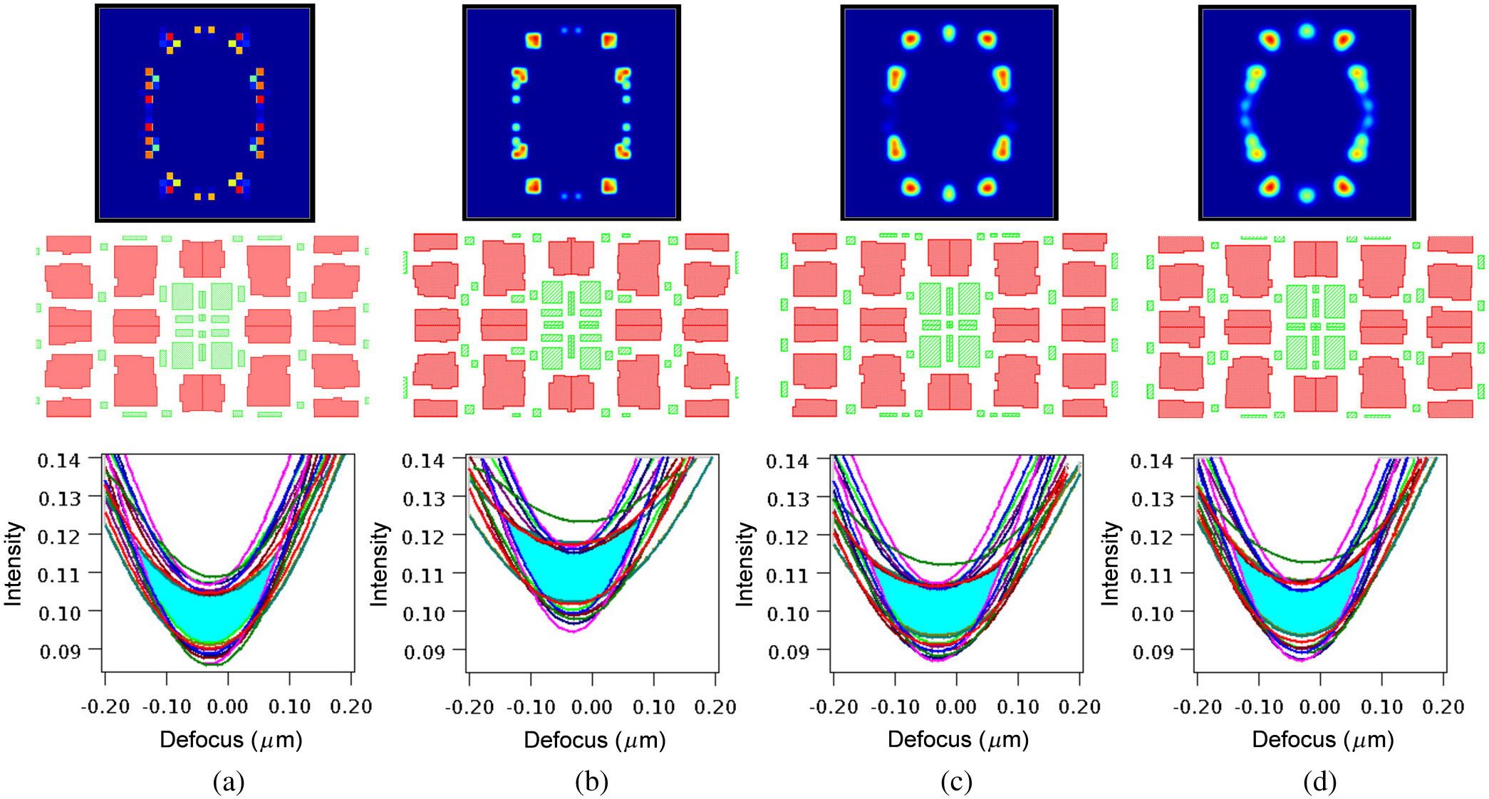 Fig. 8SMO results of various PFRs of (a) 6%, (b) 10%, (c) 20%, and (d) 30%. In each column, the upper row is the source shape, the middle one is the mask pattern with resizing and SRAF, and the lower one is the common PW. 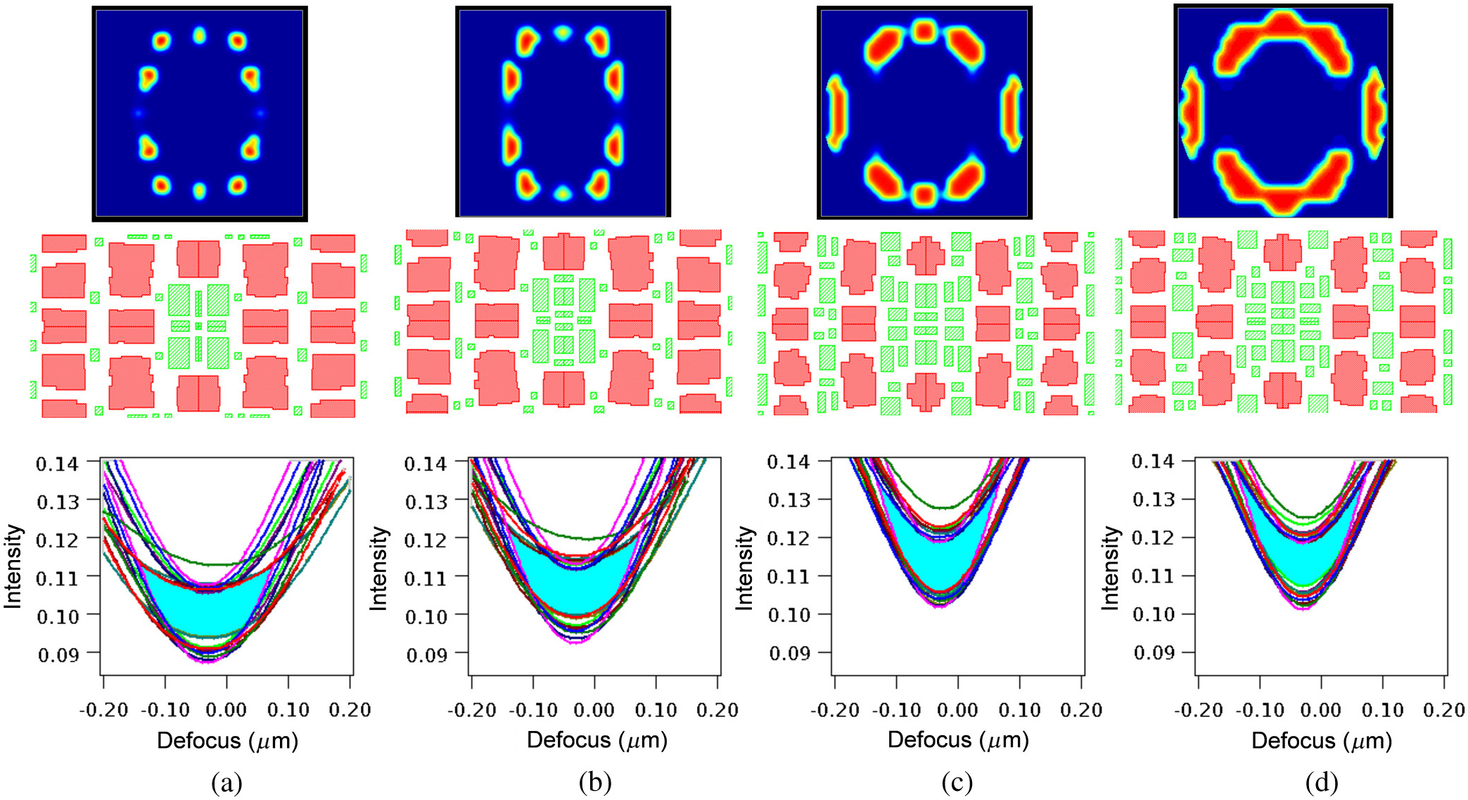 Figure 9 shows PW trees of these conditions comparing to parametric sources with OPC (see in Fig. 4). SMO successfully improved upon the OPC result for both DoF and EL on the blur dependency. When we set 6% of EL as critical dose level, DoF was increased from 93 nm to 160 nm and areas of PWs were increased around 100% on all blur values. Regarding an influence of various PFR, a common PW was exceeded to OPC results, but some degradation was observed in an area of larger PFR. Especially, PFRs of 20% and 30% were a relatively small enhancement. This might be because a larger PFR value might increase unexpected light on the grid point in the pupil. Note that PFR of the parametric source as shown in Fig. 4(a) was 15.9%, which meant that SMO could be useful with obtaining larger PW even though higer PFR values over 15.9% of PFR (e.g., 20% and 30% of PFR). MEEF values on these conditions were shown in Fig. 10. Top hat shape and over 20% of PFR might be avoided to maintain lower MEEF for an influence of mask CD error on a mask fabrication. Fig. 9PW-graph on (a) various blurs and (b) various PFRs. Areas of parametric with OPC corresponded to Fig. 4 results. 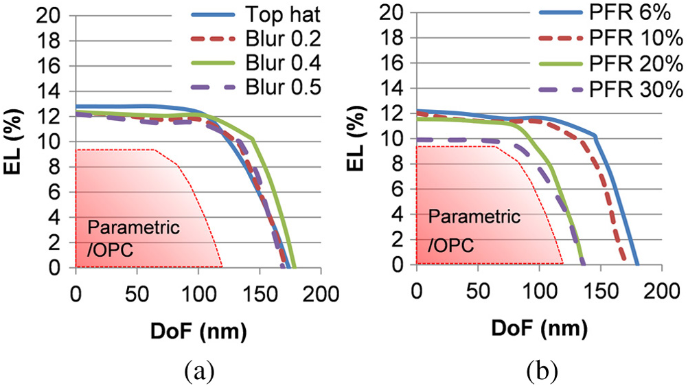 3.2.Impact of Scanners VariationFor use of the SMO solution on actual scanners, errors between the created source and the SMO target source must be considered. We assumed errors in source centering (a shift of directions for and with 1%), adjustment of the source shape (Gaussian convolution with 0.01 of illumination numerical aperture), and flare (an addition of 1% of the maximum intensity). These are exaggerated values for detecting possible imaging impacts. Figures 11 and 12 showed a dependency of the various blurs and PFRs. When the pupil flare was added to SMO target source, PW was degraded more in cases where blur was less. This indicates that usage of a calculated SMO source with a steeper profile should be careful of the effects of pupil flare in making the source on scanner. Since the source centering error and the adjusting error had no impact on PW, the SMO was considered robust for a scanner on the making sources. These trends will also help for making scanner specifications and providing recommended values of blur and PFR to users on SMO run. Fig. 11Dependency of the source making error of a shift, a shape adjustment, and a pupil flare on various blurs of (a) top hat, (b) 0.2, (c) 0.4, and (d) 0.5. 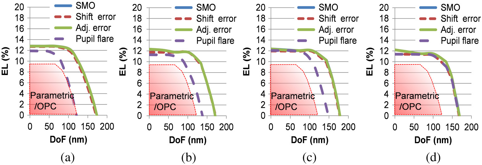 Fig. 12Dependency of the source making error of a shift, a shape adjustment, and a pupil flare on various PFRs of (a) 6%, (b) 10% (c) 20%, and (d) 30%. 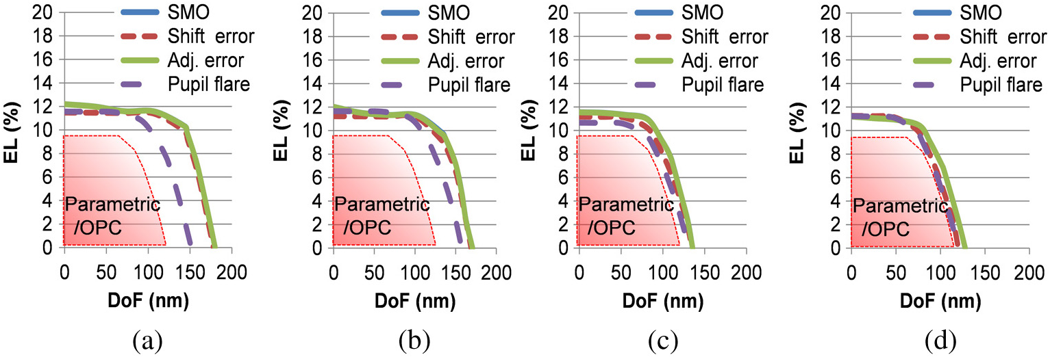 In practical use in a wafer factory for high volume manufacturing, a robust SMO source must work with a number of scanners with the same mask. Since this means that the errors of scanners cannot be fixed by OPC in the mask fabrication step, an excellent robustness should be required against the influences of some scanner variations on projection optics, and a stage vibration. So we also evaluate these impacts with aerial simulations assuming a stray light in projection lenses (an addition 1% of imaging flare), an aberration variation (an addition of wavefront error of 5 mλ RMS), and a mean standard deviation (MSD) of stage vibration between mask stage and wafer stage (a vibrating with 4 nm of mean square deviation for both and directions) for use of an SMO source. These error values were also exaggerated parameters. Figures 13 and 14 show the impacts of scanners’ variation with the various blurs and PFRs on calculated SMO. A slight impact of MSD with top hat source was observed on various blur conditions, while the other parameters had little effect on the PW. For various PFR conditions, an aberration and a stage vibration caused PW degradation in cases of sources with larger pupil fill. This phenomenon is probably because there is a large impact when aerial images had a worse profile initially. 4.Evaluation of Intelligent Illuminator Source4.1.Source Making and Its ImpactTo evaluate real pupilgrams, we made typical all sources as mentioned above on a real Intelligent Illuminator on an NSR-S621D and measured them with an in-situ detector as shown in Fig. 15. The difference of SMO targets and the measurements cannot be seen in a visual examination. Fig. 15In-situ measurement sources of (a) blur 0.2, (b) blur 0.4, blur 0.5, (d) PFR 6%, (e) PFR 10%, and (f) PFR 20%. 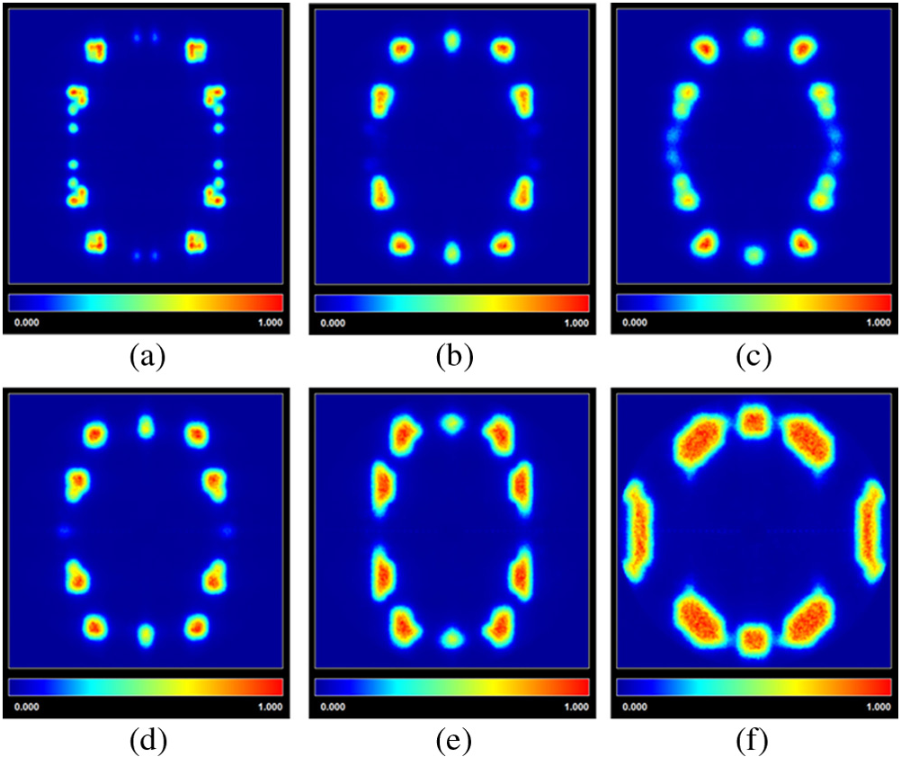 To verify the ability of the Intelligent Illuminator source making in practical use, an aerial image simulation with the measured sources instead of a target one was used. A method of CD evaluation with the simulation was used to make clear the source making error only.11 The CD variation on the patterns was calculated without any dose correction to find out real source variation. Figure 16 shows a delta CD percentage, which was suitable to explain the error contribution from with the measurement to target sources. A variation of CD below plus or minus 2%, which was target error for making source, was obtained in all simulation points. RMS errors, which included CD offset due to no dose correction on each condition were about from 0.6 to 1.2 nm. In a case of blur of 0.2, a slightly worse variation was observed. It might be an influence of pupil flare impact on smaller blur as mentioned above in the evaluation of source generation error in Sec. 3. When the data of blur 0.2 was removed, the range and a maximum RMS of the each condition were decreased to 1.5% and 0.8 nm, respectively. Fig. 16(a) Example of an evaluation pattern of drawn, SMO mask and its intensity contour and CD difference from a calculation with measured source to target one on the various conditions of (b) blurs, and (c) PFRs. 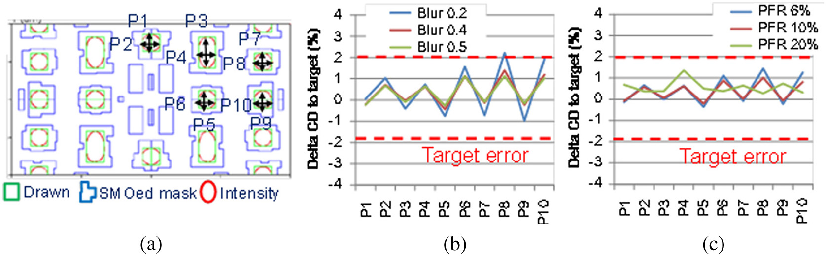 Since an evaluation of common PW with the CD simulation was more critical due to including the CD loss and degradation of each PW, the common PW-tree was calculated as shown in Fig. 17. In all the conditions of various blurs and PFRs, sufficient PW was obtained for the usage of parametric with OPC. Although it seemed that the PW of 20% of PFR was degraded relative to other conditions, it was equivalent to the case of target source (see in Fig. 9). DoF values at 6% of EL were listed in Table 1 for a numerical comparison. The values with the measurement were usable for the SMO solution compared to a parametric source case value of 94 nm. From the DoF values, a degradation ratio of the differential DoF divided by DoF on target was also listed. The ratio was successfully obtained with enough values, but there was some trend similar to pupil flare impact as shown in Figs. 11 and 12. To increase improvement, controllability with a sophisticated adjustment algorithm to target source and decreasing of measurement error would be required. Fig. 17PW graph of common PW with measurement source data with the setting of (a) various blurs and (b) various PFRs on SMO.  Table 1Depth of focus (DoF) values and degradation ratio of measurement on various SMO conditions.
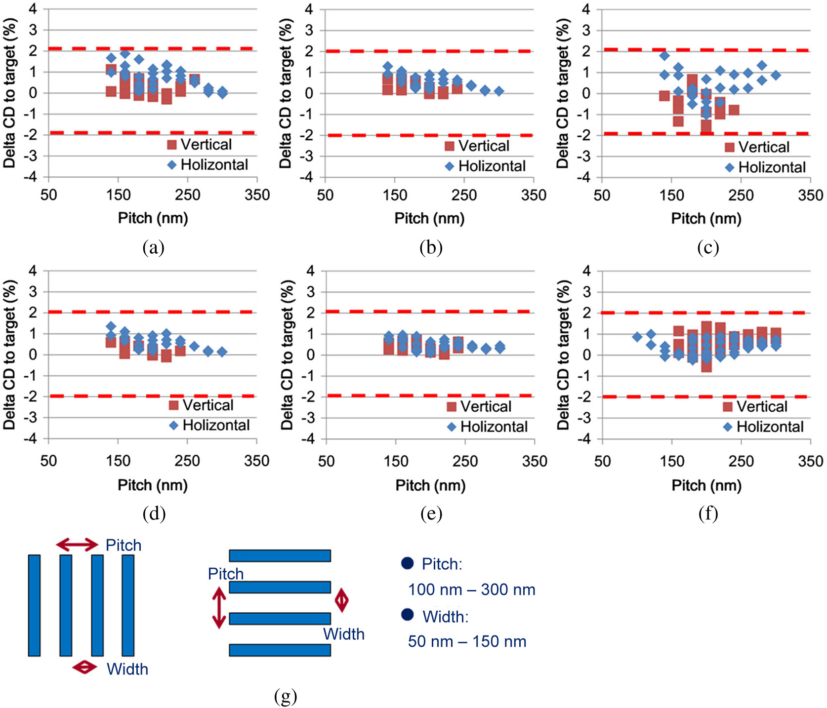
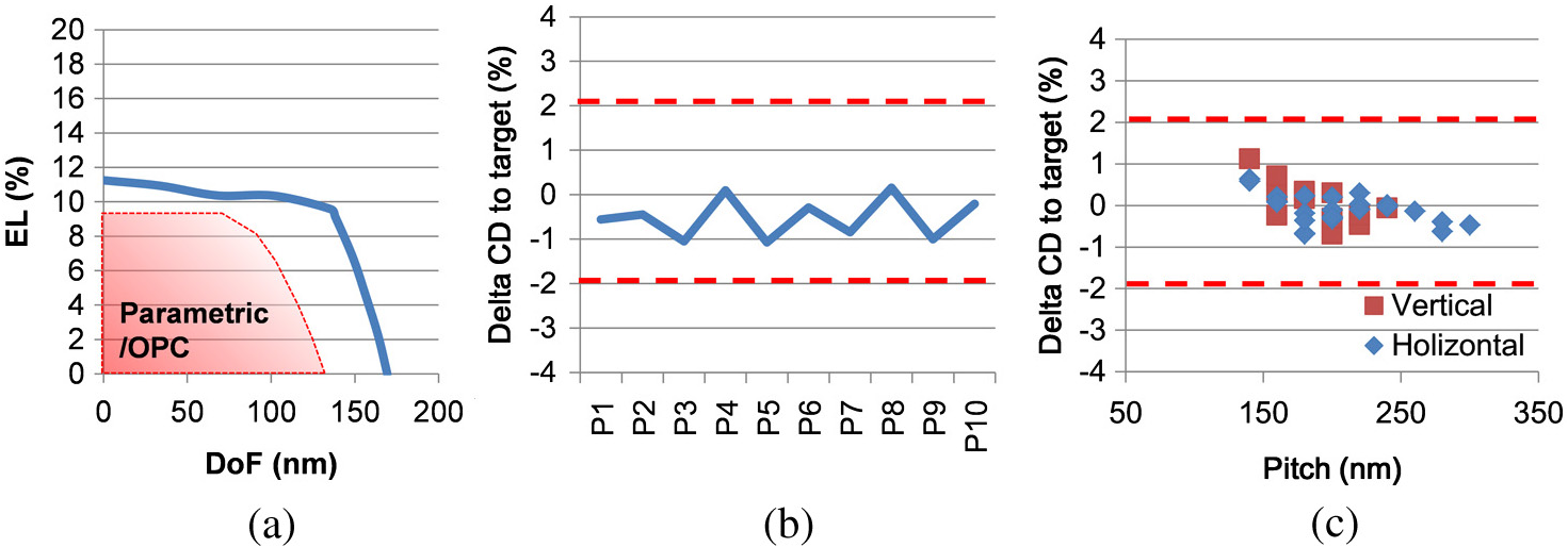
We also evaluate a CD variation in a wider variety of patterns, which will be used in a wafer production mask at the same time as SRAM insertion. The patterns were automatically generated to show effects of each source with various blur and PFR settings. Pitches and widths of one-dimensional (1–D) pattern were varied from 100 to 300 nm and 50 to 150 nm, respectively (see in Fig. 18). Figure 18 shows CD variations between the target and the measurement. All the patterns were within an acceptable range of plus and/or minus 2%. This result could support the source accuracy for full-chip pattern fabrication. 4.2.Ability of Tool-to-Tool MatchingFinally, we consider scanner-to-scanner errors in the fidelity of making a source with the Intelligent Illuminator to SMO target. As mentioned previously, in high volume manufacturing, SMO source would be used on multiple scanners with only one mask solution for reducing wafer process cost. Scanner-to-scanner variation cannot be corrected with OPC, so some variations between scanners would cause a degradation of CD and PW. The degradation in CD and PW by the variation form tool-to-tool should be anaged by SMO calculation and/or minimized with further source optimization for each scanner based on its characteristics. With knowledge of source properties from source making on scanners, a condition of 0.4 of blur and 6% of PFR was selected and made on the Intelligent Illuminator. Using the measured source data, aerial image simulation was carried out, taking into account scanner variation of actual NSR-S621D specific data, which included variation of image flare, aberration, and stage vibration as mean square deviation. Figure 19 shows the result of a PW tree of common PW and CD variations on SRAM and 1-D pattern the same as the evaluation in Sec. 3. Even though all considerable errors were in the calculation, sufficient PW and CD accuracy were obtained. We found that the method of SMO condition with the knowledge and the validation was useful for multiscanners SMO source. 5.ConclusionWe have evaluated an impact of an ability of source making with various source properties of Intelligent Illuminator on SMO. Proteus SMO, which takes into account 3-D mask, resist property with rigorous calculation, scanner fingerprint of actual scanner data, and source properties of Intelligent Illuminator, can provide usable PW with a co-optimization system and an insertion of rigorous validation on SRAM. We found that there was some dependency of the PW properties on variations of blur and PFR as well as some variation caused by source making errors on a scanner and multiple scanners’ use. This knowledge of the dependency enables us to reduce the variation by a selection of SMO solution, making the solution usable in multiple scanners with only one SMO source. Intelligent Illuminator can make sources well matched to the target of SMO. Sufficient values of the CD variations and the common PW, which were evaluated with an aerial image simulation by using in-situ pupil measurement on the scanner, revealed the ability of the system. On multiple scanners, the SMO and the making source with a consideration of the source properties can be applied through an evaluation by taking into account scanners’ variation of an image flare, aberration, and stage vibration of mean square deviation on NSR-S621D specification. The combination of the Intelligent Illuminator and illuminator-aware software makes construction of robust SMO solutions possible. ReferencesT. Mülderset al.,
“Simultaneous source-mask optimization: a numerical combining method,”
Proc. SPIE, 7823 78233X
(2010). http://dx.doi.org/10.1117/12.865965 PSISDG 0277-786X Google Scholar
K. Laiet al.,
“Experimental result and simulation analysis for the use of pixelated illumination from source mask optimization for 22 nm logic lithography process,”
Proc. SPIE, 7274 72740A
(2009). http://dx.doi.org/10.1117/12.814680 PSISDG 0277-786X Google Scholar
S. Nagaharaet al.,
“SMO for 28-nm logic device and beyond: impact of source and mask complexity on lithography performance,”
Proc. SPIE, 7640 76401H
(2010). http://dx.doi.org/10.1117/12.846473 PSISDG 0277-786X Google Scholar
T. MatsuyamaT. NakashimaT. Noda,
“A study of source & mask optimization for ArF scanners,”
Proc. SPIE, 7274 727408
(2009). http://dx.doi.org/10.1117/12.813400 PSISDG 0277-786X Google Scholar
Y. Mizunoet al.,
“Illumination optics for source-mask optimization,”
Proc. SPIE, 7640 76401I
(2010). http://dx.doi.org/10.1117/12.846476 PSISDG 0277-786X Google Scholar
T. Matsuyamaet al.,
“Application of illumination pupilgram control method with freeform illumination,”
Proc. SPIE, 8326 83260K
(2012). http://dx.doi.org/10.1117/12.916594 PSISDG 0277-786X Google Scholar
D. G. Smithet al.,
“Illuminator predictor for effective SMO solutions,”
Proc. SPIE, 7973 797309
(2011). http://dx.doi.org/10.1117/12.879116 PSISDG 0277-786X Google Scholar
T. Mülderset al.,
“Source-mask optimization incorporating a physical resist model and manufacturability constraints,”
Proc. SPIE, 8326 83260G
(2012). http://dx.doi.org/10.1117/12.914047 PSISDG 0277-786X Google Scholar
K. Patelet al.,
“IBM-JSR 193 nm negative tone resist: polymer design, material properties, and lithographic performance,”
Proc. SPIE, 5376 94
–102
(2004). http://dx.doi.org/10.1117/12.536874 PSISDG 0277-786X Google Scholar
Y. K. Tyminskiet al.,
“Impact of scanner signatures on optical proximity correction,”
Proc. SPIE, 7640 76400V
(2010). http://dx.doi.org/10.1117/12.845061 PSISDG 0277-786X Google Scholar
G. McIntyreet al.,
“Qualification, monitoring, and integration into a production environment of the world’s first fully programmable illuminator,”
Proc. SPIE, 7973 797306
(2011). http://dx.doi.org/10.1117/12.879483 PSISDG 0277-786X Google Scholar
BiographyHajime Aoyama received his PhD degree from Tohoku University. He joined Fujitsu Limited in 1989, where he carried out research on optical, electron, proximity X-ray, and extreme ultraviolet lithography. He joined Nikon Corporation in 2011. Since then, he has been engaged in the development of strategic solution on immersion lithography. Yasushi Mizuno received a BS degree in mechanical engineering from Tokyo University of Science in 1996 and MS degree in mechanical engineering from the same university in 1998. In the same year, he joined Nikon Corporation in Japan. He is a senior system designer for imaging system of the exposure tool. He is now working for the illumination system development for state-of-the-art ArF immersion scanner. Noriyuki Hirayanagi received his MS degree in applied physics from the University of Tsukuba. He joined Nikon Corporation in 1994. He has been working on the development of the exposure tools for advanced lithography, such as electron projection lithography, extreme ultraviolet lithography, and ArF immersion lithography. Naonori Kita received his BS degree in physics from Tokyo University of Science in 1998 and his MS degree in Tokyo Institute of Technology in 2000. In the same year, he joined in Nikon Corporation and his interests are in optics design and the optical impacts on microlithography. Ryota Matsui is a researcher in Optical Research Laboratory at Nikon Corporation. He received his PhD in applied physics at Osaka University in 2007. His research interests include computational lithography, convex optimization, and optical microscopy. Hirohiko Izumi received his PhD degree in material science from the Tokyo Institute of Technology. He worked for DRAM process development in Nippon Steel and Yield Management Consulting in KLA Tencor. He joined Synopsys in 2007 and he is now responsible for the application engineering of lithography simulation. Keiichi Tajima is a corporate application engineer with the Silicon Engineering Group in Synopsys, Japan. He has more than 10 years experience in software development and 18 years in lithography simulators. Joachim Siebert received his PhD degree in astrophysics from the Technical University Munich. He joined SIGMA-C in 2004, which was acquired by Synopsys in 2006. Since, then he has been working in the Sentaurus Lithography group, mainly being responsible for SMO, EUV lithography, and resist calibration. Wolfgang Demmerle is a product marketing manager for lithography simulation solutions at Synopsys, which he joined with the SIGMA-C acquisition in 2006. His previous work experience includes engineering positions at Nikon and ASML. He received a doctor degree in semiconductor physics from the Technical University of Munich. Tomoyuki Matsuyama received a BS degree in applied physics from the University of Electro-Communications in 1989. In the same year, he joined Nikon Corporation. He has been working in the area of optical design and manufacturing technology development for microlithographic lens. Recently, he is working on development of application software for the imaging system of a lithography exposure tool. He is currently a manager of the Strategic Imaging Solutions Section, Precision Equipment Company. |
||||||||||||||||||||||||||||||||||