|
|
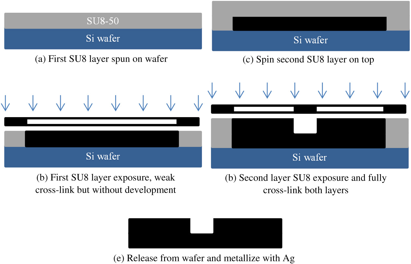
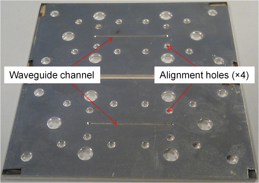
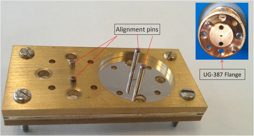
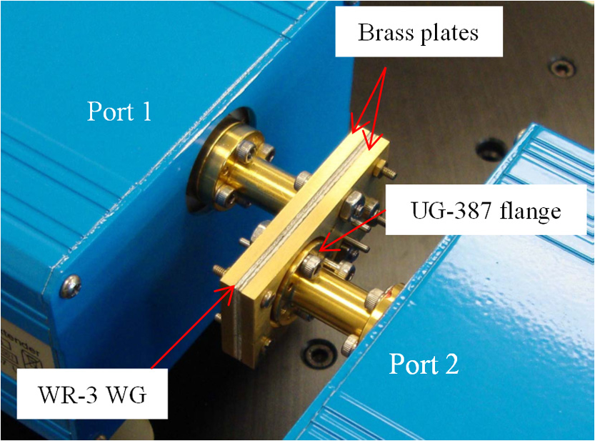
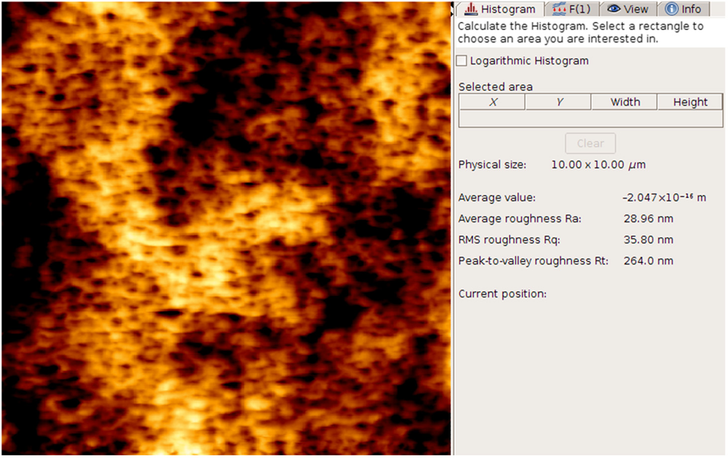
1.IntroductionMillimeter-wave and terahertz components in the frequency range from 100 GHz to 10 THz have been finding more and more application prospects. Examples of application areas include medical imaging, ultrafast wireless communication, and security scanning.1 At such high frequencies, the components for processing the microwave signals need to have a high-dimensional accuracy and very smooth surface to achieve minimum signal attenuation or energy loss in the transmission line. The transmission loss, usually termed as insertion loss (IL), is commonly used to indicate this signal attenuation through the device so that the lower IL presents better performance. A waveguide is usually a hollow air-filled structure to convey electromagnetic waves and is a critical component in microwave systems. The conventional way of making waveguides is precisely controlled CNC metal milling.2 However, with the increase in the operating frequency, the dimensions become smaller (the cross section of the waveguide here is only ) and it is more and more challenging to machine and sometimes impossible to make some of the complicated structures inside the waveguide. Therefore, new manufacturing routes have been sought to meet the increasing demand of terahertz waveguides requiring extremely high-dimensional accuracy and surface smoothness. For microwave applications, the frequency of 300 GHz represents a cusp in the current technology development where industrial development is progressing rapidly at lower frequencies () but no matured technology is available for higher frequencies. Hence, success in fabricating a 300 GHz device will provide a benchmark for producing other devices at higher frequencies. Thick SU8 photoresist can be used as the structural material for constructing waveguides as it offers good dielectric properties and cost effectiveness, has a good repeatability and requires low facility investment in comparison with the precision CNC milling. In our previous studies, SU8 photolithography process has been successfully used for fabricating low frequency waveguides, filters, and slot antenna.3–6 However, as the frequency increases, there is less space for the manufacturing tolerance and more work is needed to meet the requirements of high-dimensional accuracy, extreme surface smoothness, and low transmission loss. Typically, the WR-3 (220 to 325 GHz) rectangular waveguide is equally divided into four layers, as shown in Fig. 1(a), with each layer having a nominal thickness of 432 μm. The cross section of the waveguide is which was split along the long edge of the waveguide to minimize losses. In order to enable measurement of this 300 GHz rectangular waveguide, two back-to-back right-angled bends, acting as the input and output ports, were designed to connect with the network analyzer measurement system, as shown in Fig. 1(b). It should be noted that, in order to connect the measurement system, accurate alignment is required between the WR-3 waveguide bends now on the upper and lower surfaces of the structure and the measurement port. This is extremely accurately achieved in this case by having the waveguide precision alignment pin holes formed in the SU8 itself, making the alignment as accurate as the photolithographic process. Fig. 1Illustration of WR-3 waveguide structure with the right angle bends: (a) three-dimensional structure of the device and (b) the waveguide structure where the blue represents air in the reality. 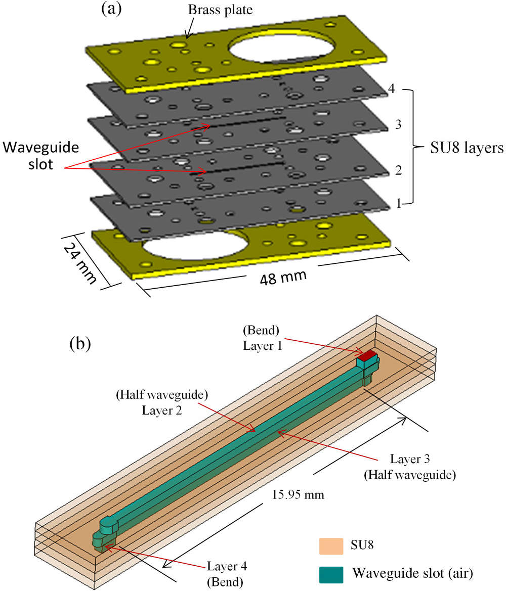 The entire waveguide (excluding the bends) is 15.95-mm long. Previously, the four layers were fabricated separately in SU8 then metalized with silver, bonded together using adhesives, and finally assembled using two brass plates7,8 for support. As shown in Fig. 2, this method will create three interfaces between the four layers which would give a number of positions where the air gaps could occur. It has been realized that the air gaps between SU8 layers have a deleterious effect on device performance which results in current leakage and higher transmission loss. Fig. 2Cross-sectional view of the WR-3 waveguide which consists of four layers. Each layer is designed as 432-μm thick. and . The red stands for the silver metallization. 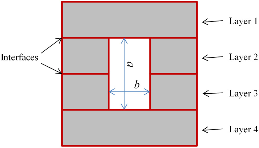 A double-layered SU8 processing technique was, therefore, explored to reduce the IL. Instead of making the four SU8 layers individually, the four layers were combined into two double layers and each was fabricated through one process. Then, the interfaces between layers 1 and 2 as well as layers 3 and 4 were eliminated due to the cross-linking effect of the SU8. Hence, the chances for any possible air gaps will be significantly reduced, as there is now only one interface, i.e., between layers 2 and 3. This process has been successfully applied to a straight waveguide and the IL was noticeably reduced.9 In this paper, we present the first WR-3 (220 to 325 GHz) waveguide with back-to-back right angle bends having ultralow IL similar to the CNC machined metal circuits. The SU8 fabrication process will be detailed and the performance of the device will be demonstrated and discussed thereafter. 2.FabricationThe SU8 process is illustrated in Fig. 3. The first layer of SU8-50 was spun on a 100-mm silicon wafer where the thickness was controlled by weighing the material. In this case, 5.2 g SU8-50 was needed to achieve the required thickness of 432 μm and the amount was derived out of previous calibration. Due to the excessive thickness, the edge bead needs to be removed to improve the uniformity. The wafer was then placed onto a carefully leveled stage for a few hours for self-planarization of the SU8. SU8-50 was used as it has relatively lower viscosity and flows more easily on the wafer compared with other formulations, such as SU8-100 or 250. After that the wafer was baked at 65°C for 30 min followed by baking at 95°C for 270 min. It should be noted that, in order to minimize the residue stress in SU8, a slow temperature ramp (i.e., at ) is always necessary during the heat-up process while the wafer is cooled down naturally to room temperature after bake. Once the wafer was cooled down after soft bake, it was exposed in a Cannon PLA-510 mask aligner. Typically, the light coming out of the UV lamp consists of three main lines at 365, 405, and 436 nm. It is known that the long wavelength UV light has the ability to penetrate deeper into the SU8, but is less effective in inducing the photo acid for cross-linking. First, the wafer was exposed with a L39 filter so that only the lines above 400 nm could pass through to achieve deep penetration and a 2-min interval between each of the 40 s was adopted to stabilize the resist. After the first set of exposures, a PL360 filter was used, which allow the i-line 365 nm to pass through, to expose the wafer for another with 2-min interval as well. Then, a postexposure bake (PEB) was conducted at 70°C for 15 min to form a weak cross-link. It is noted that the development was not needed at this stage. The second layer of SU8-50 was spun on top of the first layer with the same weight of 5.2 g. The wafer was baked at 70°C for 8.5 h. A relatively lower bake temperature was adopted to minimize the stress accumulated in the ultrathick SU8 layers, but for a longer time. The cross-link of the first layer was reinforced during the second bake as well. After the bake, the wafer was exposed for through the mask following the same strategy mentioned above. Alignment marks were transferred to the first layer during the first exposure and were used to ensure the second layer was reproduced in the same position. PEB then proceeded with a higher temperature of 95°C for 30 min to form strong cross-link in both layers. The whole piece, consisting of two-exposed layers, was thereafter developed in EC solvent for 45 min assisted by vigorous magnetic stirring agitation. After that, the wafer was hard baked at 110°C for 15 min. During the exposure of the second layer, the long wave UV light was able to penetrate both SU8 layers and therefore a strong cross-link was formed to seamlessly bond the two layers together. The SU8 was then released from the wafer substrate by putting into 10% NaOH solution for a few hours. The final product was one-half of the waveguide, i.e., either layers 1 and 2, or layers 3 and 4. Once the half-waveguide was released and cleaned, a Cressington 308R metal evaporator was utilized to deposit silver on the half-waveguide. The sample was first cleaned by oxygen plasma for 30 s, and then 100 nm Cr was deposited as an adhesive layer. To ensure a good performance, silver was evaporated on the SU8 to a thickness of 2 μm, ensuring a good conductivity and giving a sufficiently large microwave skin depth. To achieve a full coverage on the sidewalls, the sample was tilted to 30° and rotated during the evaporation so that the sidewalls were fully covered by silver. The final waveguide pieces are shown in Fig. 4. In order to investigate the repeatability of the process, two devices were made and compared in this study. Figure 5 shows the details of the waveguide bend constructed by this two-layered SU8. A small negative slope was observed along the sidewall due to the shadowing effect during exposure. After optimization, the process was able to produce 432-μm thick SU8 with the tolerance of 10 μm. Fig. 5Details of the waveguide bend formed by the two layers SU8 process. (a) Close view of the right-angle bend in layer 1 and excellent alignment between the two layers, (b) small angles along the sidewall in layer 2 due to the shadowing effect. 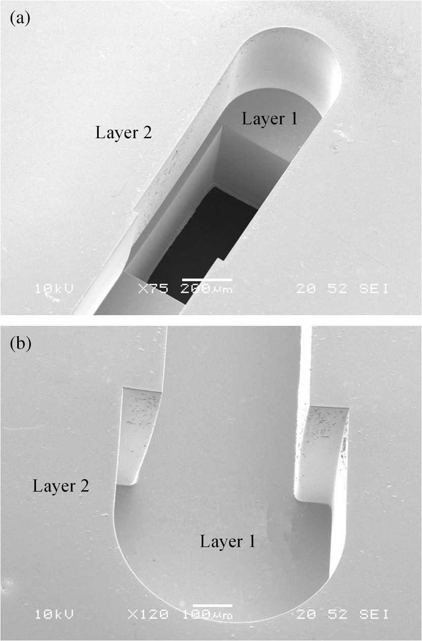 After silver coating, the device was ready to assemble in the measurement jig. Two brass plates were made to provide strong mechanical support and allow the device to be easily handled and accessible to the measurement kit. The silver-coated SU8 pieces were stacked in the order shown in Fig. 1(a) and clamped between the two brass plates. Four accurate 1.6-mm diameter metal pins were pushed through the SU8 layers to ensure the accuracy of alignment. Figure 6 shows the assembly of the device and the configuration of the matching UG-387 flange on the measurement kit. The brass plate was only for support and provided no part in the accurate alignment of the measurement waveguide. 3.Measurements and DiscussionsThe measurements were carried out on an Agilent E8361A Network Analyzer with OML WR-3 extension T/R module at test port 1 and a receive-only T module at test port 2, as shown in Fig. 7. A one-port calibration and a response calibration were performed before measurements. Four alignment pins were carefully pushed through the waveguide and the flanges to provide accuracy in positioning. Screws attached to the flanges went through the waveguide and into nuts on the other side of brass plates to provide secured connections. The scattering matrix is employed to describe the microwave properties of a circuit and the measurements determine the -parameters. -parameters, i.e., and , are generally used to present the transmission () and reflection () from a two-port microwave components and are usually expressed as decibels (dB). For a waveguide, with the two ports numbered as ports 1 and 2, describes the reflection coefficient or return loss, i.e., how much signal is reflected back to port 1 when port 2 is terminated with a matched load. The parameter is the transmission coefficient or IL of the devices referenced from port 1 to port 2. For an ideal microwave transmission (i.e., no IL), would have a transmission coefficient of 100% (i.e., 0 dB). In a real system is desired to be as small as possible. Figure 8(a) shows the measured -parameters of the double-layered SU8 waveguides compared with the simulated results. It can be seen that the IL is only around 0.5 dB over a wide frequency range from 220 to 300 GHz. As shown in Fig. 8(b), with an expanded scale, the IL was below 0.45 dB in the higher frequency range between 260 and 300 GHz. This represents a loss of only over this frequency range. Such a low IL is comparable to the typical results of between 0.015 and obtained from the precise CNC machined waveguides reported in Refs. 2 and 5. As shown in Fig. 8, the measured IL corresponds to an equivalent coating conductivity of , which is around 30% of the conductivity of silver block (). The return loss was about 10 dB which was fairly good for this device. Moreover, the results revealed excellent repeatability of this technique as the measurements of the two devices almost overlapped each other. Additionally, it is believed that the discrepancy in measured of two devices is due to the imperfectly slight miss alignment between two halves. The doweled pins utilized here can offer an alignment tolerance of 20 μm.9 The alignment accuracy of the first device is slightly worse. This leads to the first device’s slightly poorer return loss (), as is sensitive to the alignment accuracy. Fig. 8(a) Measured and performance of the double-layered SU8 WR-3 waveguides comparing with the simulation results. (b) is a zoom-in view of . The simulation employs an effective conductivity of . 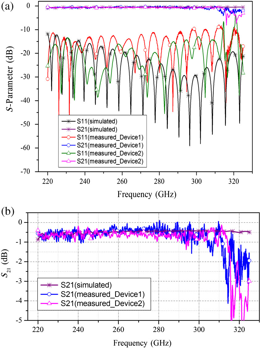 The thickness uniformity of the SU8 layers plays an important role in determining the success of this process. The edge bead effect is an intrinsic phenomenon of spin coating where the thickness of photoresist gradually increases from the center to the edge of the wafer. Adjacent to the very edge, there can be excessively thick photoresist. This fact was taken into account during the double-layer SU8 fabrication process and the edge bead was removed immediately after spin coating. The wafer was then placed on a leveled stage to rest for a few hours and, during this resting time, the SU8 would perform a self-planarization due to its surface tension. In this study, the thickness variation was controlled below 10 μm across the entire device area which is believed to be an important contribution to the excellent performance. In addition, the surface roughness is another crucial factor regarding the IL of the waveguide. Due to the scattering of electrons, the silver surface with a rough finish will increase the conductor loss and therefore deteriorate the IL. According to Refs. 10 and 11, the additional loss caused by surface roughness can be determined as where is the loss (in dB) of a conductor with a root mean square (rms) surface roughness of , is the loss of a conductor with an ideal smooth surface without any roughness, is the skin depth of the conductor, and is the normalized surface roughness.The roughness of the evaporated silver on the double-layered SU8 WR-3 waveguide was examined using atomic force microscopy (AFM), as shown in Fig. 9. An rms roughness was obtained below 40 nm. Substituting a value of 40 nm into Eq. (1), is calculated to be . (without considering surface roughness) is obtained as from the microwave calculations. In this calculation, the conductivity of silver (i.e., ) and an operating frequency of 300 GHz are employed. Therefore, it can be concluded that this surface roughness does not have significant impact on the SU8 waveguide’s performance. 4.ConclusionA multilayered SU8 fabrication process has been successfully developed and utilized for the first time to produce a WR-3 waveguide with ultralow IL. This technique eliminates the interfaces between layers 1 and 2 as well as between layers 3 and 4, and therefore reduces the probability of air gaps trapped at the interface. The IL over 220 to 310 GHz is measured as 0.028 to which is comparable with CNC machined metal circuits, (0.015 to ). Additionally, this process is highly repeatable and has shown to be a promising scenario for making more complicated terahertz circuits, especially for those finding difficulties in CNC machining process. AcknowledgmentsThe work is supported by the UK Engineering and Physical Science Research Council. The authors would like to thank M. Ke for contribution to one of the devices presented in this paper. The interferometer used in this research was obtained through Birmingham Science City: Innovative Uses for Advanced Materials in the Modern World (West Midlands Centre for Advanced Materials Project 2), with support from Advantage West Midlands and part funded by the European Regional Development Fund. ReferencesI. Hosakoet al.,
“At the dawn of a new era in terahertz technology,”
Proc. IEEE, 95
(8), 1611
–1623
(2007). http://dx.doi.org/10.1109/JPROC.2007.898844 IEEPAD 0018-9219 Google Scholar
A. R. Kerret al.,
“Loss of gold plated waveguide at 210–280 GHz,”
ALMA Memo, 585 1
–6
(2009). Google Scholar
M. Keet al.,
“Micromachined rectangular coaxial line and cavity resonator for 77 GHz applications using SU8 photoresist,”
in 2008 Asia-Pacific Microwave Conf.,
1
–4
(2008). Google Scholar
Y. WangM. KeM. J. Lancaster,
“Micromachined 38 GHz cavity resonator and filter with rectangular-coaxial feed-lines,”
IET Microwaves Antennas Propag., 3
(1), 125
–129
(2009). http://dx.doi.org/10.1049/iet-map:20080011 1751-8725 Google Scholar
N. A. Muradet al.,
“Micromachined H-plane horn antenna manufactured using thick SU-8 photoresist,”
Electron. Lett., 46
(11), 743
–745
(2010). http://dx.doi.org/10.1049/el.2010.1054 ELLEAK 0013-5194 Google Scholar
N. A. Muradet al.,
“Micromachined millimeter-wave Butler matrix with a patch antenna array,”
in 2009 Mediterranean Microwave Symposium (MMS),
1
–4
(2009). Google Scholar
X. Shanget al.,
“Micromachined WR-3 waveguide filter with embedded bends,”
Electron. Lett., 47
(9), 545
–547
(2011). http://dx.doi.org/10.1049/el.2011.0525 ELLEAK 0013-5194 Google Scholar
X. Shanget al.,
“Measurements of micromachined submillimeter waveguide circuits,”
in 2010 76th ARFTG Microwave Measurement Conf.,
1
–4
(2010). Google Scholar
X. Shanget al.,
“WR-3 band waveguides and filters fabricated using SU8 photoresist micromachining technology,”
IEEE Trans. Terahertz Sci. Technol., 2
(6), 629
–637
(2012). http://dx.doi.org/10.1109/TTHZ.2012.2220136 ITTSBX 2156-342X Google Scholar
I. Mehdiet al.,
“A broadband 900-GHz silicon micromachined two-anode frequency tripler,”
IEEE Trans. Microwave Theory Tech., 59
(6), 1673
–1681
(2011). http://dx.doi.org/10.1109/TMTT.2011.2123112 IETMAB 0018-9480 Google Scholar
M. V. LukicD. S. Filipovic,
“Modeling of 3-D surface roughness effects with application to coaxial lines,”
IEEE Trans. Microwave Theory Tech., 55
(3), 518
–525
(2007). http://dx.doi.org/10.1109/TMTT.2007.891688 IETMAB 0018-9480 Google Scholar
BiographyYingtao Tian received the PhD in mechanical engineering from Loughborough University, UK, in 2010. His research focused on miniaturization of microelectronics, advanced electrochemical fabrication and precise manufacturing. After 2 years research in fabrication of terahertz microwave circuits in University of Birmingham, he is currently a research associate with the Department of Materials in University of Manchester. His present research interests are advanced processing of light alloys for aerospace applications. Xiaobang Shang received the PhD degree in microwave engineering from the University of Birmingham in 2011. He is currently a research fellow with the School of Electronic, Electrical, and Computer Engineering, The University of Birmingham, UK. His present main research interests are laser micromachined millimeter-wave and submillimeter-wave waveguide circuits, mode-matching technique for waveguide components, the design of multiband filters and multiplexers, and the integration of antenna and filter. Michael J. Lancaster is a fellow of the IET, UK, and the UK Institute of Physics. He is a chartered engineer in the UK, and chartered physicist in the UK. He has served on the IEEE MTT IMS technical committee. His present research interests include microwave filters and antennas, the high frequency properties and applications of a number of novel and diverse materials. He has published two books and over 170 papers in refereed journals. |