|
|
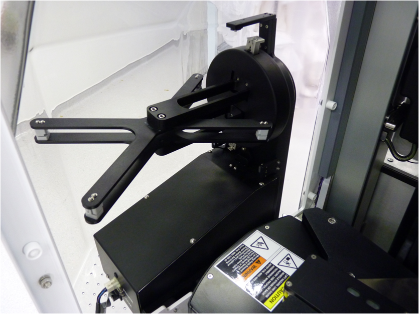
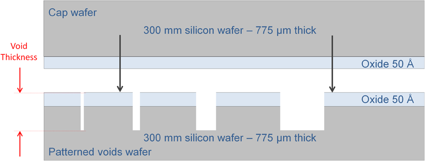
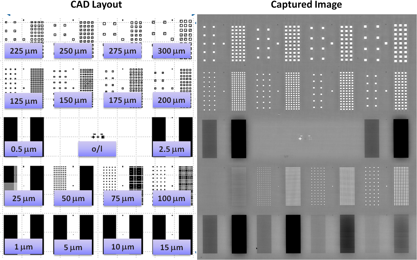
1.IntroductionFor many years, ongoing requirements for increased computational power at increasingly higher device-packaging densities were accomplished by shrinking the sizes of the basic devices themselves to ensure higher degrees of integration. In the last few years, three-dimensional (3-D) integration has emerged as a complementary method to feature-size scaling to achieve the performance improvement, in which integrated circuits are stacked together in order to improve power consumption, reduce resistance–capacitance delays, decrease device form factor, provide heterogeneous integration, and increase bandwidth, allowing the most efficient process technologies to be used for the various types of devices. One embodiment of this architecture stacks multicore central processing unit (CPU) units with memory devices in the same package. Several process flows have been proposed for manufacturing 3-D integrated circuits, commonly referred to as via-first, via-mid, and via-last.1,2 Each of these 3-D technologies requires new wafer-level process technologies to be added to the process flow. These process steps include fabrication of through-silicon vias (TSV), wafer thinning, and either temporary or permanent wafer bonding. 1.1.Motivation for Void DetectionBonding is a key step in 3-D integrated circuit fabrication, occurring in multiple steps during the fabrication process. There will be a permanent bonding process during final assembly—which may be a wafer-to-wafer, chip-to-wafer, or chip-to-chip procedure—this will be using a process such as oxide-to-oxide, Cu-to-Cu, or adhesive bonding. In addition, there may be a temporary bonding step, where a device wafer is temporarily bonded to a handle wafer to permit the wafer thinning and other process steps. For the via-last process, the vias are formed after the wafer is thinned (note that in the via-first and via-mid processes, the vias are formed before or during the device and interconnect process). Each bonding process requires a strong, uniform bond, which is free of voids. These voids can occur from a number of chemical or mechanical processes including trapped air, solvent evaporation, outgassing from the polymer during curing, or particulates and surface nonuniformities. Such voids can interfere with the mechanical stability of the interface, causing unwanted local topology variation, nonuniform thinning, which can affect the TSV reveal process yield, or even delamination and breakage during thinning. Additionally, voids that occur during final assembly applications may interfere with electrical connectivity. 1.2.Process Flow DescriptionIdentification and characterization of bond voids have prompted a search for appropriate high-volume manufacturing metrology tools, to be used to scan each of the various bond interfaces described above for voids. The Inspection and Metrology Task Force of the SEMI 3D Stacked IC Committee has initiated round-robin experiments to investigate the capabilities of various metrology tools to detect and/or characterize voids between wafers.3 The first of these experiments uses bonded wafer pairs, produced at SEMATECH, which are patterned with sets of programmed voids. The wafer pairs are produced using the following process steps: a 5-nm oxide layer was grown on the top surface of both the patterned wafer and the cap wafer. A 70-nm SiN film, followed by an organic underlayer, was deposited on the wafer designated as the void wafer. Photoresist was deposited and after developing, the wafer was etched to one of the four predetermined depths, using the organic underlayer and SiN as hard masks. The patterned and unpatterned wafers were oxide bonded after wet clean and surface plasma activation. Since these wafers do not have metallization or other materials that would be found on device wafers, this experiment is intended to provide a baseline for the capabilities of various metrology techniques. Most of the techniques involved in this experiment, including the one described in this article, are expected to be limited in their ability to identify voids between the interfaces in bonded stacks of patterned wafers. Also, note that these voids differ from voids caused by in-process variations, such as particles, trapped gas, etc., as described above, and the voids do not induce stress in the wafers at the region of the void. The technique described in this article does not depend on measuring stress to identify and characterize the void, allowing these patterned voids to stand in for “real” voids in this experiment. Finally, please note that none of the current metrology tools proposed for void detection are thought to be capable of detecting the actual particles that cause voids; the best expected performance is to be able to detect the voids, which are many times the size of such particles. 2.Instrument DescriptionThis article reports on a technique under development using infrared (IR) microscopy4,5 to identify and characterize the voids. The absorption edge of silicon is approximately 1 μm, which means that the IR wavelengths are necessary for the wafers to be transparent and hence for the voids to be seen by the microscope.6 Since this technique uses reflected IR microscopy, it is expected to be especially useful for temporary bonding processes where the interface can be imaged through the unpatterned carrier wafer. The technique is particularly interesting given its relatively simple setup and fast detection with reasonable spatial and depth resolutions. As will be shown in this publication, good progress has been made in applying IR microscopy to bonding interface void detection. Good correlation to known void dimensions is demonstrated, and the technique’s limit of detection is explored by varying void diameter, density, and depth. Further work is ongoing to integrate the technique into a fully automated metrology tool. The work presented in this publication has shown IR microscopy to be a promising technique for detecting and measuring geometries of wafer-to-wafer bonding interface voids. A basic diagram of the instrument can be seen in Fig. 1. The instrument has a broadband IR light source that is incident onto the wafer, through an optical filter and a beam splitter. Optical filtering is performed using a 1-μm high-pass filter in sequence with a 1.3-μm low-pass filter, resulting in a wavelength range of 1.0 to 1.3 μm. For detection, an indium gallium arsenide line camera is used, which has good sensitivity in the 1.0 to 1.7-μm wavelength range. Since silicon is transparent in the IR, the instrument is capable of detecting and measuring voids through the top silicon wafer, which is typically thick. The objective lens assembly contains a lens exchanger, which is fitted with lenses of varying magnifications for resolving different size features. The objectives used for image acquisitions to date have magnifications in the range of to apertures of 0.1 to 0.65, and field of view from 8 to 0.8 mm. The camera pixel size calibration is performed by measuring an object of known size in micrometer to determine its size in pixels. After the calibration has been performed, the lateral dimensions measured by the microscope are directly reported during the measurements. The system includes a wafer flipper, as seen in Fig. 2, in order to enable the inspection of the wafer through the bottom substrate. Handling of the wafer is done with edge gripping, and the wafer stage used is a high-precision stage. The microscope images are acquired using the line camera, which has its detector array oriented perpendicularly to the primary scan direction of the stage. The width of the field being scanned therefore depends both on the size of the line array and the magnification of the lens objective being used. Along the scan direction, the image is created by stitching consecutive line image captures as the wafer is scanned at constant speed under the lens objective. The stage motion controller is used to generate a trigger signal for image acquisition. When the stage has moved a predetermined scan length a trigger signal is sent to the line camera, which is synchronizing image acquisitions with the movement of the stage. This predefined scan length, corresponding with the time between triggers, is set so that the pixel size in the scan direction equals the pixel size in the direction along the line camera. The acquisition of a single line starts when the trigger signal is received by the camera. The exposure time is therefore set to be somewhat shorter than the time required for the stage to travel the distance between two triggers. The two measurement modes available are full and partial wafer scans. For partial wafer scans, the images are captured from predefined areas of the wafer, which regions may be configured to represent dies on the wafer or to cover areas of the wafer that are prone to have voids in the bonding process. The length of the scan is therefore dependent, on which one of the two measurement modes is being used. In case of full wafer scans, the scan length is determined by the wafer boundaries and is therefore dependent on how close to the center of the wafer it is being acquired, whereas for the partial scan mode it is determined by the width of the fields to be scanned. Since the size of scanned areas is generally larger than the field of view of the line camera, a final image is composed of multiple image scans that are stitched together with a small overlap, ensuring full coverage of the scanned area. The actual time needed for a full wafer scan is dependent on which magnification the objective lens is being used, since higher magnification results in smaller pixel size and smaller field of view. Using a microscope objective, a full wafer scan takes approximately 10 min, while a full wafer scan using a microscope objective requires a little over 1 h. It is therefore useful to be able to control the magnification with the goal to keep the measurement time as short as possible for a given void feature detection wafer scan. The depth of field (DOF) of the imaging system is dependent on the magnification lens objective used. For the magnification, the DOF is greater than 100 μm, while for the magnification it is a few micrometers. Since the wafer is supported by its edges, there is some sagging of the wafer toward its center. Experience has shown the DOF to be sufficient to resolve a complete field of view, but re-adjustment of the focus height is needed as the wafer is being scanned, and several types of autofocus systems are currently being evaluated for the final metrology tool. The basic void detection principle is based on the fact that a reflection can occur at the transition in different refractive indices. In this case, because the void has relatively lower refractive index compared to the silicon dioxide bonding material, it gives a different reflectance than the surrounding material. As a result, the amount of light reflected at the bonding interface is different in areas where the voids are present, allowing the voids to be detected by the IR microscopy instrument. An example of this is shown in Fig. 3. Fig. 3Principle of IR microscopy: the mismatch in refractive index due to the presence of a void results in greater reflection. 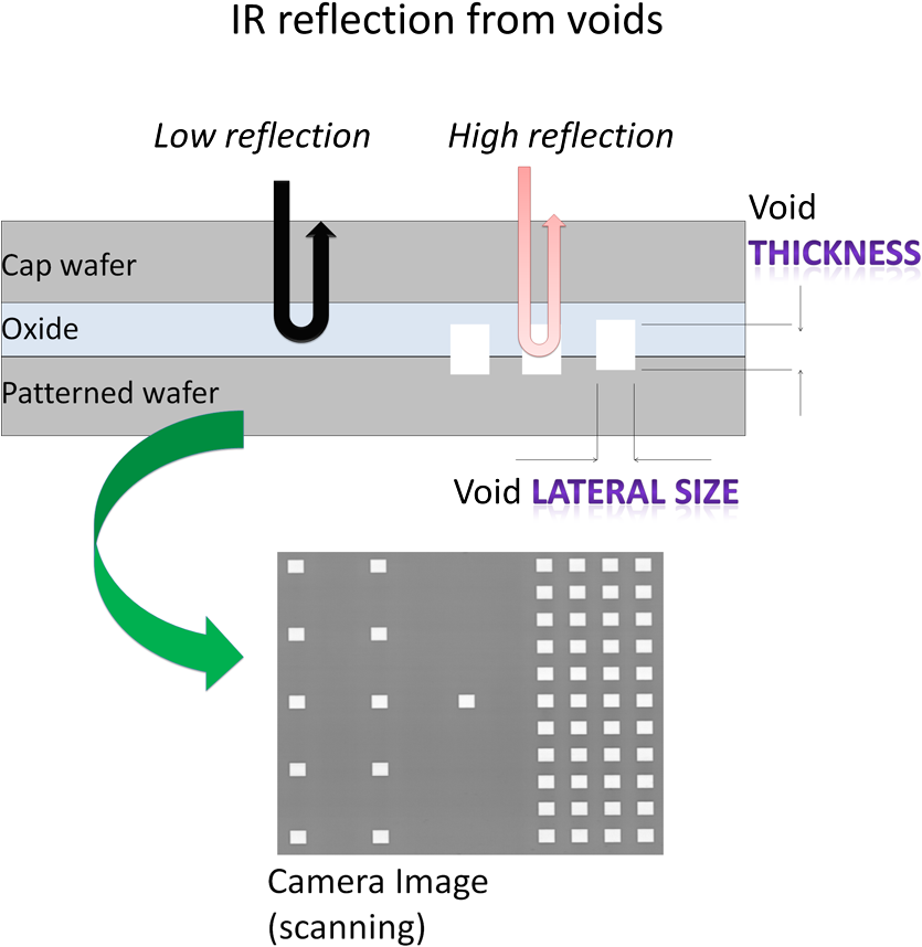 The horizontal geometry of the voids can be determined directly by measuring the voids seen on the indium gallium arsenide (InGaA)s camera. An example of intensity linescan across a void is shown in Fig. 4. As can be seen, the intensity is around its maximum value for a considerable portion of the void diameter, and there are minima near the edges of the void, which have somewhat lower intensity than the background. To determine the lateral size of a single void, we used a 30% intensity threshold edge-detection algorithm. The results obtained from the experiment using this method were found to be in good agreement with nominal designed dimensions for various void sizes, and good numerical stability was achieved when calculating the diameter of different voids of the same size. The distance found is scaled using the pixel size calibration before reporting the void size as the measurement result. Fig. 4Linescans across 275-μm wide void features, showing the minimum intensities near the edges. 40-, 400-, 800-, and 1200-nm void depths from top to bottom (45% of original image scale).  In order for voids to be measureable, they need to be resolvable and detectable. Detecting void defects can be done by inspecting an acquired image for intensity changes that are not part of the intentional pattern of the sample being inspected. In order for a detected void to be resolvable, it needs to be separated in the acquired image from neighboring voids. Examples are included in the experimental results for larger areas of multiples voids that are detectable, but with pitch too small for individual voids to be resolvable or measureable. The measurement algorithm used allows reporting of dimensions and locations for voids that are resolvable and at least three pixels in size. 2.1.Automated Void Detection MethodThe approach for detecting and measuring voids is different in the case of the experiment with the wafers from SEMATECH containing intentional voids and in cases where unintentional voids are present on patterned production wafers. In both cases, a wafer coordinate system is required. By aligning the wafer using the notch and edges prior to the measurement, the sample position and orientation on the stage can be corrected, and the coordinate system with the origin in the center of the wafer can be defined. In the case of the experiment with the SEMATECH wafers, the pattern itself consisted of the voids to be detected and a given die was requested to be scanned. After aligning the wafer and scanning the requested die, each pixel in the image can be converted into a position in wafer coordinates. Knowing the die structure from the computer-aided design (CAD) layout, the dense, semi-dense, and isolated void areas of the captured image with various void sizes can be inspected to detect the voids and measure their dimensions, and wafer or die coordinates and brightness information can be extracted. In the case where unwanted voids are present on an intentional pattern, the structure of the pattern can also be recognized on the wafer. By scanning each of the dies to be measured and merging them into one master die, the intentional die pattern can be removed; by subtracting the master pattern from the individual die maps, residual void images are generated. Each significant feature from the residual images is treated as a defect, which can be classified according to the properties that are extracted from the captured image such as position and intensity distribution. General characteristics of voids found in these cases are approximately circular in shape and have intensity distributions that are dependent on the void size and depth. 3.Sample DescriptionThe wafer set consists of four bonded wafer pairs, which are formed using standard thickness (775 μm) 300-mm wafers that are bonded together using a 5-nm oxide layer, using the process flow as described earlier. As shown in Fig. 5, one of the wafers in each pair was patterned with programmed voids. These programmed voids have diameters ranging from 0.5 to 300 μm. The voids on each of the four wafer pairs were etched to different depths ranging from 40 to 1200 nm. In addition, the voids are present in isolated, semi-dense, and dense formats, as shown in the CAD layout included in the left part of Fig. 6. 4.Experimental ResultsThe right part of Fig. 6 shows the captured image on a die with approximately 400-nm deep voids. The image capture was performed using a lens objective with magnification or pixel size. In this configuration, the image size obtained by one scan is . To image one die, five overlapping scans were performed, of which the middle area was used for each scan. Therefore, the resulting matched image (Fig. 6, right) is . From the image, all the voids in semi-dense ( space:width) and dense ( space:width) arrangements are detected, but for smaller void sizes, the individual voids cannot be resolved. From Fig. 7, which is showing images from the same image capture at original image scale, we can see more clearly how the smallest resolvable void depends on density and lateral dimensions. As the voids get smaller and thinner, they become more challenging to detect in isolated arrangement and to resolve in regions with increased void density. Fig. 7(a) Original scale images of 40-nm deep voids, captured with a objective: 2.5-, 5-, 10-, and 15-μm lateral sizes from top to bottom. For this void depth, a 10-μm detection limit was observed for isolated areas, while all semi-dense and dense voids can be detected but cannot be individually resolved. (b) Original scale images of 400-nm deep voids, captured with a objective: 2.5-, 5-, 10-, and 15-μm lateral sizes from top to bottom. For this void depth, all voids were detected for isolated, semi-dense, and dense areas but all of them were not individually resolved. (c) Original scale images of 800-nm deep voids, captured with a objective: 2.5-, 5-, 10-, and 15-μm lateral sizes from top to bottom. For this void depth, all voids were detected for isolated, semi-dense, and dense areas but all of them were not individually resolved. (d) Original scale images of 1200-nm deep voids, captured with a objective: 2.5-, 5-, 10-, and 15-μm lateral sizes from top to bottom. For this void depth, all voids were detected for isolated, semi-dense, and dense areas but all of them were not individually resolved. 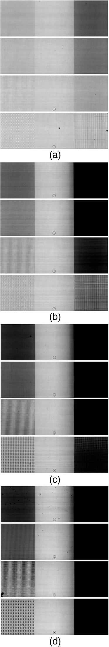 A summary of the smallest detectable, resolvable, and measurable voids for samples with varying void depths is included in Table 1. For the lens objective measurements, the 40-nm deep voids were observed to have a 10-μm detection limit for isolated areas. As the void depth increases to 400 nm or thicker, the smallest detectable void decreases to 2.5 μm for isolated voids, whereas in case of semi-dense and dense areas the detection limit is 0.5 μm. The smallest resolvable 40-nm deep void lateral sizes were found to be 10 μm for semi-dense and 15 μm for dense areas, while a 5-μm resolution limit was found for all other depths. The smallest automatically measurable void size for 40– to 800-nm deep voids was 25 μm for all regions. As it is seen in Fig. 4, 1200-nm deep voids have lower contrast with respect to the background, which leads to unstable measurements of the size of the 25-μm voids, and therefore a 50-μm measurement limit is recorded for this depth. Using the magnification objective lens ( pixel size), voids as small as 0.5 μm can be detected. In semi-dense areas, voids as small as 0.5 μm can be resolved, while only 2.5 μm ones can be resolved in dense areas. Automatic size measurements were not performed using images. Table 1Summary of the smallest detectable, resolvable, and measurable voids for samples as a function of void depth and density.
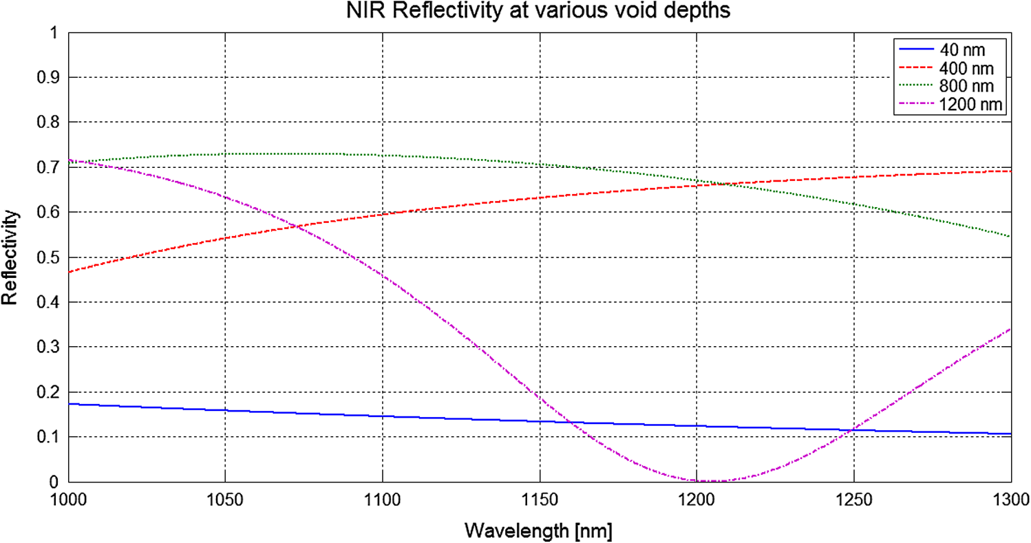
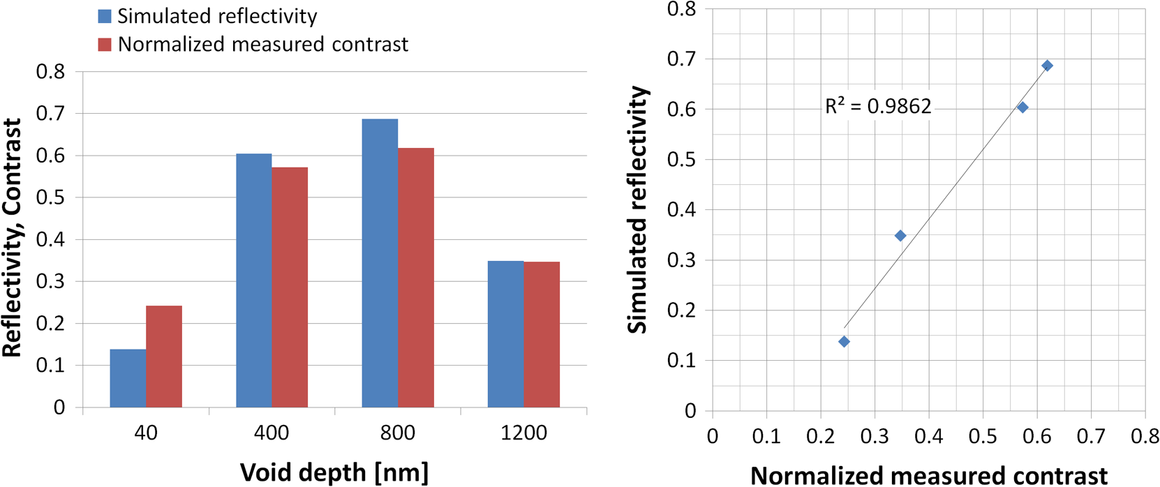
Lateral void dimension measurement fidelity was evaluated by correlating the lateral dimensions measured by the IR microscopy instrument with the nominal (design) dimensions. As shown in Fig. 8, the results are in good agreement with -square for all the void depths. From the results, we also note that the slope is generally close to unity, indicating that the instrument’s pixel size calibration is in good agreement with the nominal designed dimensions. One exception is the 1200-nm deep voids, for which the slope is 0.94. This is not yet fully understood. Further work is ongoing to measure the sister wafers using other techniques, which may help to give a better understanding. While the intentional voids greater than 1-μm deep that are etched in silicon for the DOE wafers are interesting for exploring instrument sensitivity, the bonding voids that pose practical issues in the semiconductor fab manufacturing line are typically formed in the bonding interface. Fig. 8Correlation between lateral dimensions measured by the IR microscopy instrument versus the nominal dimensions based on the CAD layout. These results are based on data of isolated voids. Measurements on top left voids (and their nearest neighbors) in semi-dense and dense arrangements resulted in same values within measurement error. 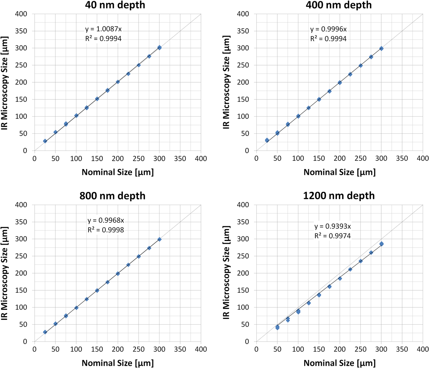 In order to further explore the sensitivity to void depth, reflectance simulations were performed for void depths on the DOE wafers (40, 400, 800, and 1200 nm).7,8 For the simulations, a 0-deg angle of incidence was used with a filmstack from bottom to top as follows: infinite silicon substrate, air (varied thickness), 5-nm silicon dioxide, and 775 μm of silicon. As shown in the simulation results in Fig. 9, reflectance is expected to increase from 40 to 800 nm, but for 1200-nm depth, antireflective behavior is observed with lower average intensity. It should be noted that in this study, the focus has been on voids that are formed in the lower part of the oxide bonding layer. Additional future work exploring the effect of bonding interface void depth on instrument sensitivity could be beneficial. Results shown in Fig. 10 indicate that the intensity contrast is sensitive to the void depth, and good correlation is observed. The contrast was calculated as the normalized range in intensity measured across the voids. A future study may be performed to determine whether the measured contrast together with precalculated reflectance versus void thickness data can be reliably used to determine the void thickness. 5.ConclusionsThe IR microscopy has been evaluated for detecting and measuring the dimensions of voids that are formed in the oxide-to-oxide interface of permanently bonded programmed void wafers. Results have demonstrated that the technique has the required sensitivity to detect and measure the isolated and dense voids of horizontal dimensions varying in range from submicron up to hundreds of micrometers and depths varying from 40 up to 1200 nm. The capability to acquire the images, inspect them for void defects, and measure the found voids with reasonable speed makes the technique a good solution for high-volume manufacturing implementation in semiconductor fabs. The IR microscopy instrument is currently being integrated into a fully automated platform in order to build a tool suitable for tier 1 fab production implementation. The method is expected to have immediate application to temporary bonding applications, where the imaging can be done through the carrier wafers. Additional work will be needed to investigate the applicability to permanent bonding applications, where the presence of surface metallization and TSVs (for via-first and via-mid processes) may prevent imaging of the bond plane. Work is also being pursued to explore whether combining IR microscopy with other techniques, such as photoluminescence or model-based Fourier transform infrared (FTIR) reflectometry,9 will be beneficial for improved inspection and metrology capability in a manufacturing metrology tool. Future work to take advantage of algorithms previously developed is desirable to more accurately report dimensions.10,11 AcknowledgmentsHan Chang is acknowledged for fruitful discussions regarding the bond void detection experiment. ReferencesHandbook of 3D Integration, Wiley-VCH, Weinheim
(2008). Google Scholar
J. H. Lau, Through-Silicon Vias for n3D Integration, McGraw-Hill Professional, New York, NY
(2012). Google Scholar
R.A. Allenet al.,
“Intercomparison of methods for detecting and characterizing voids in bonded wafer pairs,”
ECS Trans., 33
(4), 581
–589
(2010). http://dx.doi.org/10.1149/1.3483550 1938-5862 Google Scholar
R.W. Ditchburn, Light, Dover Publications Incorporated, New York
(1961)). Google Scholar
E. Hecht, Optics, 3rd ed.Addison-Wesley, Reading, Massachusetts
(1997). Google Scholar
E. D. Palik, Handbook of Optical Constants of Solids, Academic Press, San Diego, California
(1997). Google Scholar
R. M. A. AzzamN. M. Bashara, Ellipsometry and Polarized Light, North-Holland Physics Publishing, Amsterdam
(1987). Google Scholar
G. E. Jellison Jr.,
“Data analysis for spectroscopic ellipsometry,”
Thin Solid Films, 234
(1–2), 416
–422
(1993). Google Scholar
P. C. S. HayfieldG. W. T. White,
“Ellipsometry in the measurement of surfaces and thin films,”
Natl. Bur. Std. Misc. Publ., 157157
(1964). Google Scholar
D. LeCunfJ. HöglundN. Laurent,
“In-line metrology of high aspect ratio structures with MBIR technique,”
in Advanced Semiconductor Manufacturing Conference (ASMC),
(2011). Google Scholar
D. NyyssonenR. D. Larrabee,
“Submicrometer linewidth metrology in the optical microscope,”
J. Res. Natl. Bur. Stand., 92 187
–204
(1987). http://dx.doi.org/10.6028/jres.092.017 JRNBAG 0160-1741 Google Scholar
C. F. VezzettiR. N. VarnerJ. E. Potzick, Antireflecting-chromium linewidth standard, SRM 475, for calibration of optical microscope linewidth measuring system, 260
–117 NIST Special Publication, Gaithersburg, Maryland
(1992). Google Scholar
BiographyJonny Höglund is managing the Semilab USA applications group and is working with metrology and inspection equipment used for material characterization and process monitoring, primarily in the semiconductor and photovoltaic industries. In 2004, he joined Philips AMS, where he worked with surface acoustic wave and MBIR metrology, and he is working with Semilab since the merger in 2009. He has been active in the semiconductor industry for 13 years and previously worked with ASML. Zoltan Kiss joined the optics group of Semilab in 2010 as a developer working with metrology and inspection equipment used for material characterization and process monitoring, primarily in the photovoltaic and semiconductor industries. Between 2001 and 2010, he worked in Hungarian Astronomical Research Institutes on Measurement Automation, Development, Image and Data Analysis in international cooperation. He gained a PhD degree on related topics in the Eötvös University, in 2009. Gyorgy Nadudvari leads the optics development team at Semilab Inc., working on optical inspection and metrology technologies both in semiconductor and photovoltaic industries. In 2007, he joined Semilab, and runs projects including infrared inspection of bulk microdefects in silicon, photoluminescence, and photomodulated reflectance metrology. Earlier, he worked in the area of optical development, inspection, and manufacturing in other companies, including Philips Optical Storage. He holds an MSc degree in engineering physics. Zsolt Kovács has worked at Semilab, Hungary, since 2012 in the optics group and is dealing with the development of optical methods for the characterization of material and manufacturing defects in semiconductor or photovoltaic samples. From 2009 to 2012, he worked at the Research Institute for Solid State Physics and Optics in Budapest, dealing with optical investigation of flowing phenomena in granular materials. He gained the MSc degree as a physicist in the Eötvös University, in 2012. Szabolcs Velkei has managed the software development group in Semilab since 2013. He is heavily involved in R&D of image processing techniques and data processing. He established his own company in 2005 and is primarily concerned with artificial intelligence development. He joined Semilab in 2012. Chris Moore received his PhD in physics in 1983 and after a brief period of teaching, where he concentrated on instrument development and measurement technologies, he was one of the founders of Waterloo Scientific Inc. in 1985. He has worked in all facets of the metrology industry from product development through marketing and sales to technical and business management. His last position was with Semilab USA as president and CEO. Victor Vartanian is a metrology engineer at SEMATECH in the 3D Interconnect Division. Prior to joining SEMATECH, he worked at Motorola/Freescale on applications of strained silicon to transistors. Previously, he worked on applications of FTIR and mass spectrometry to environmental issues in semiconductor manufacturing and in process development. He received his BS and PhD degrees in chemistry from the University of Texas at Austin. He has numerous publications and 10 patents in the semiconductor field. Richard A. Allen is a physicist at NIST, where his research focuses on metrology for 3D stacked ICs and MEMS. He leads the SEMI 3DS-IC Standards Committee and was NIST assignee to SEMATECH’s 3D Enablement Center from 2011 to 2013. Prior to joining NIST, he developed test methods for in situ characterization of space radiation effects at JPL. He received the BS and MS degrees from RPI and his MBA degree from Columbia Union College. |
|||||||||||||||||||||||||||||||||||||||