
|
|
1.IntroductionThe 2011 International Technology Roadmap for Semiconductors expanded on the requirements for metrology of three-dimensional (3-D) interconnects to include wafer alignment, interface bonding, and through-silicon vias (TSVs).1 TSVs play a very important role in vertically connecting upper-layer circuits and lower-layer circuits in 3-D integration. One of the main challenges for 3-D metrology involves measuring TSVs etched at a very high aspect ratio (HAR) of etch depth to via diameter, approaching to . These HAR features challenge and limit the use of optical metrology techniques for measuring smaller-diameter TSVs. Recently, a number of metrology tools have become available that are capable of supporting in-line TSV etch depth measurement in high-volume manufacturing, such as various types of interferometers and confocal microscopes.2–5 However, these are sensitive to aspect ratio and are not typically able to make reliable measurements of TSV etch depth for vias in the range of a few microns wide by several tens of microns deep. The maximum measurable depth increases with the size of the via’s critical dimension (CD) opening and decreases with the objective’s numerical aperture (NA). As the via diameter decreases, the aspect ratio increases, and there are few known noncontact measurement techniques that are suitable for in-line inspection. One example uses a scanning white-light interferometer with a small imaging aperture and low NA illumination to scan the objective perpendicular to the surface to generate signals for in-line TSV depth measurement.6 However, the signal from the top surface and the thin buried film are merged if there is a monolayer or stacked layers on top of the TSV sample, which commonly occur. Thus, a more advanced algorithm is required for accurate TSV depth measurement. Another example uses a backside infrared interferometric technique for sensing the thickness of a wafer for HAR vias 1 and 5 μm in size; there is no sidewall interference to inhibit optical techniques, and thus, the infrared sensor’s accuracy and repeatability are independent of the aspect ratio of the via.7 However, the illumination spot size (either 15 or 5 μm) limits the transverse resolution. If two or more vias are closer together than a spot size, then the depth of each via is difficult to measure independently. A similar infrared light interferometric technique was reported to be capable of nondestructive direct depth and bottom shape measurement of TSVs with diameters as low as 1 μm.8 However, if the backside of the wafer is illuminated with infrared light, then it is easily scattered by the convex bottom shape, except for a very small portion of light that is aimed exactly at the limited flat center area of the via bottom, which can reflect back to the optics unit. Thus, it is very challenging to apply the backside infrared interferometric technique to determine the curved bottom shape, especially on the scale of a few microns. Reflectometry techniques have gained wide acceptance in semiconductor manufacturing processes for monitoring the dielectric film thicknesses and lithographic linewidths of two-dimensional and 3-D structures.9–13 The normal-incidence spectral reflectometer is an excellent tool for the characterization of TSV depths and shapes. Horie et al. developed a UV-reflectometry technique for fast trench-depth measurement. They calculated the reflected light by comparing the area ratio of the complex amplitude reflectivity returned by the top surface and trench regions.14,15 In our previous studies, we demonstrated the use and enhancement of this existing wafer metrology tool by implementing a novel theoretical model and measurement algorithm for HAR TSV measurements.16,17 TSV manufacturing process with high etch rate stages combined with efficient passivation or deposition steps have achieved nearly anisotropic shapes, with high etch rates of 5 μm/min or greater.18,19 Good etch depth uniformity and shape requirements for 3-D integration are necessary in a high-volume manufacturing process. Variation in via protrusion due to nonuniformities in TSV etch depth can have a significant impact on via node resistance.20 As the etch rate increases, the ability to control the wafer temperature becomes crucial to obtaining a uniform etch across the wafer, regardless of the wafer diameter.21 The current standard technique for measuring and controlling the uniformity of HAR vias is to use a cross-sectional scanning electron microscope (SEM) analysis. Samples are cleaved to yield a cross-sectional view. This is somewhat accurate for confirming the shape of the structure. However, if the cleaving line for the cross-section is not straight, or if the cross-section is not perpendicular to the line, then the SEM measurement results, especially for the vertical depth, tend to be inaccurate and not repeatable. Moreover, the sampling is very limited as it is time-consuming, in addition to being destructive and costly. Thus, it is limited to monitoring uniformity of TSV depth across wafers, which is important for development of an etching process. The possibility that one could make via depth measurements nondestructively and extremely fast opens up the possibility of mapping the variation of via depth within an illumination area and across an entire wafer (from center to edge). In this work, we present a methodology for testing the reflectometer-based depth measurement linearity on a calibrated step height over a range of 5 to 100 μm. We verify the accuracy of TSV depth measurement with cross-section SEM over a depth range of 30 to 60 μm. In this paper, we refine the previous published model of the reflectance spectrum based on a modified thin film model, where the ratio of illuminated surface areas is adjustable, and use amplitude modulation algorithms to extract the via depth, bottom shape, and roughness. Updated TSV measurement results from actual wafers formed from 3-D interconnect processing with greater aspect ratios and smaller via CD size are presented. The potential for verifying the accuracy of measurements of the via depth with cross-section SEM will be discussed. 2.Samples and Instrumentation2.1.TSV and Step Height SamplesThree different groups of TSV samples formed from actual 3-D interconnect processes were studied. These TSV targets consisted of
A reference standard with six nominal step heights of 5, 10, 30, 50, 75, and 100 μm was used.22 2.2.Reflectometer ConfigurationThe TSV structures were measured using an unmodified Nanometrics 9010B reflectometer tool, and the reflectance spectrum was measured in a broadband wavelength range from 375 to 780 nm. This reflectometer is a nearly normal-incidence system equipped with two different objectives ( and ) and an automated translation stage, primarily developed for thin film thickness and optical CD (OCD) measurements. A low-magnification () and low-NA (0.035) microscope objective was used in this study. The normal-incidence measurement largely relies on interference between light scattered from different locations on the target structure. To measure the via depth, the light waves reflected from the top and bottom of the via target structure must interfere with each other. The reflectance spectrum typically has a regular oscillation over a large wavelength range. The limiting factor in this case is the pixel resolution of the charge-coupled device (CCD) detector, which is at the upper wavelength limit of 780 nm. 3.Theoretical Model of Reflectance SpectrumWe simulate the reflectance spectrum based on the scalar diffraction model as the size of the via opening is much greater than the probing wavelength. Thus, we can account for effects of the via by simply calculating the path difference between the wavefront reflected by the unetched top surface regions and the wavefront reflected by the etched via regions. In the case of vias of similar size as the incident wavelength, another approach involving electromagnetic vector diffraction models is needed for an exact simulation of the reflectance spectrum. This solves the rigorous coupled-wave solution, which requires intensive computation. In this work, we focus on the simplified scalar diffraction model, which provides fast calculation speed with reasonable accuracy. 3.1.TSV Array StructureThe via structure is modeled as a film with an adjustable ratio of the illuminated surface areas. When illuminating beam spot moves across the via arrays target, the intensity of reflected light oscillates due to vias moving in and out of beam spot. Mata-Mendez and Chavez-Rivas23 have estimated that for grating with line-to-space ratio of , the amplitude of oscillation becomes negligible when the minimal number of gratings inside the beam spot is two, which is corresponding to 50% of the illuminated surface areas. For the HDTSV array structure of few microns via size, the ratio of the illuminated area of the top silicon surface to the via’s opening within the illuminated area is considered to be constant, and it depends only on the via’s opening shape and pitch. The illumination spot covers a number of vias: most of the vias are entirely illuminated; only few of them under the spot edge are partially illuminated. Although illumination spot might slightly move with respect to array between repeated measurements, the influence on the total area of vias varies little, and therefore, the variation of intensity of reflected light can be neglected. Assuming a particular value for the ratio, the coefficients and () are the portion of the illuminated top silicon surface and the via opening, respectively, is the electrical field incident on the silicon surface and the via area, the via depth is , and the wavelength is . The reflectance intensity , which is the sum of the two reflected beams from the silicon surface and the via bottom surface, is The third term of Eq. (1) indicates that the electrical field reflectances must be combined using their proper phase angle differences. According to the Fresnel equation, light propagating through the air that reflects off a silicon surface will undergo a 180-deg shift, and its electrical field reflectance will be influenced by a reflecting factor, . The simulated reflectance intensity can be calculated by multiplying by the reflecting factor . 3.2.Via Bottom RoughnessBennett and Porteus24 provided a theoretical expression and experimental verification showing that if light of a sufficiently long wavelength (compared to the surface roughness) is reflected from a rough surface, then the decrease in measured specular reflectance due to surface roughness is a function of only the root-mean-square height of the surface irregularities. where is defined as the root-mean-square deviation of the surface from the mean surface level, is the specular reflectance of the rough surface, and is that of a perfectly smooth surface of the same material. Undesirable surface roughness is quite likely to occur because it is naturally formed by the plasma etching process. Because the top surface is mirror-like Si wafer or a thin oxide film in the other case, thus, the wavelength-dependent attenuation factor caused by roughness applied to the reflectivity of vias only. Thus, we further modified the reflectance intensity of Eq. (2) by combining it with Eq. (3) to yield the following equation:3.3.TSV Array with Oxide Hard MaskOne common form of an HAR silicon via has an oxide hard mask on top of it; this can result in interference if multiple-reflected light waves interfere constructively. We define as the optical thickness of the oxide film, which corresponds to the physical thickness . The refractive index of oxide, , is a constant of 1.46 over our measured wavelength range (375 to 780 nm). The refractive index of silicon varies with the wavelength range (from 6.706 at 375 nm to 3.696 at 780 nm).25 The light incident on the surface of the oxide film divides into reflected and refracted portions. The refracted beam reflects again at the oxide film-silicon interface. Part of the light may reflect internally again and continue to experience multiple reflections within the oxide film layer until it has lost its intensity. The electrical field reflecting from the oxide film can be expressed according to the following equation for multiple reflections in thin-film interference. where is the reflection coefficient from the top of the oxide film, is the transmission coefficient from air into the oxide film, is the reflection coefficient from the oxide-silicon interface, is the transmission coefficient from the oxide into the air, and is the reflection coefficient from the oxide-air interface back into the oxide film. In this case, the light signal drops to in an internal reflection within the oxide film layer.263.4.Via Bottom ShapeA key feature of a small diameter HDTSV is that the etching process generates a curvature at the bottom of the via. We account for this by using a half-oblate spheroid model, as shown in Fig. 1 and given by Fig. 1Schematic of via, with cross-sectional view (a) and top view (b). Effective area of bottom, with diameter , contains depth variations that are below depth resolution limit . 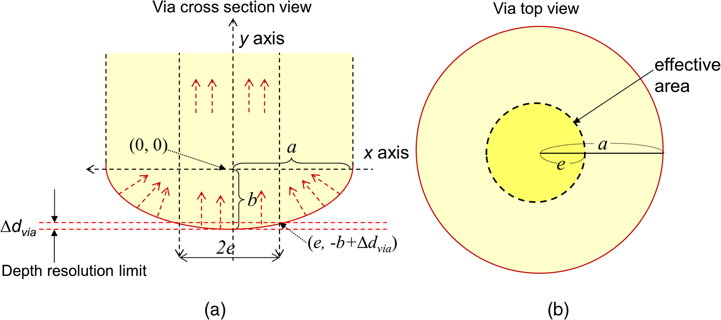 With this, the via bottom shape can range from a perfect flat disk (minor axis length ) to a half-round spheroid (, where is the major axis length). Although the bottom of a small diameter via is curved, a great fraction of the light incident on the curved bottom surface is scattered and cannot be reflected back to the top surface. However, it is still possible to obtain an attenuated interference spectrum because the depth variations around the center area of the bottom are quite small, which means that it can be considered as a flat surface for partially reflecting normally incident light waves back to the top surface. We developed a reflectance modulation algorithm for extraction of the via bottom shape from the measured reflectance spectrum.16 We assume an effective area of the bottom, with a diameter of , that contains depth variations that are sufficiently small and below the resolution limit of depth measurement of the measuring tool. We use a simple method to estimate the measurement resolution from the pixel resolution. The relationship between the via depth resolution () and the pixel resolution () of the CCD detector can be derived from the equation (where is an arbitrary integer), when the two reflected beams from the top silicon surface and the via bottom surface constructively interfere, resulting in the equation The depth resolution decreases with the total depth of the structure, but it improves with the upper limit of the wavelength. A pixel resolution of 0.6 nm is typical for an normal incidence (NI)-OCD system. By taking the nominal via diameter as the horizontal, transverse diameter () at the oblate equator in Eq. (6), the vertical, conjugate radius can be obtained if one set of coordinates on the oblate trajectory is known. If (0, 0) is the center of the oblate spheroid, then the radius of the effective bottom area and its position relative to the center equatorial plane () are used as one set of and values in Eq. (6), respectively. Thus, the effective radius decreases because of the increasing vertical radius ; in addition, a smaller amplitude of interference oscillations is expected. The electrical field reflecting from the via bottom, as taken from part of Eq. (4), can be expressed as The ratio of the effective illumination area in the via bottom area to the top via opening area is expressed as . Thus, we further modified the electrical field of Eq. (9) to yield Eq. (10). Although the attenuation factor () does not contain the minor axis parameter directly, it can be obtained by means of Eq. (8). The combined total reflectance spectrum can be calculated as . The simulation spectra of Fig. 2(a) are based on a via array structure of 30.0 μm depth and 3.0 μm CD, and an oxide hard mask of 423 nm thickness is on top of the array surface. The via bottom is assumed to be perfectly smooth () and flat (). Because thickness and depth information is primarily contained in the frequency of intensity oscillations, two oscillation frequencies corresponding to the thickness of oxide hard mask and the depth of vias are clearly visible in the reflectance spectrum. Deeper vias will exhibit a greater number of oscillations over the given wavelength range, while thinner films will exhibit fewer oscillations over the same range. Figures 2(b) and 2(c) address two effects of parameters: the surface roughness and minor axis length . Figure 2(b) assumes a minor axis length of (flat bottom) and shows the reflectance spectrum with surface roughness values of 50 and 100 nm according to Eq. (3). The spectra are strongly attenuated with increasing surface roughness, especially at the shorter wavelengths (). Figure 2(c) assumes via with a bottom roughness of and shows the reflectance spectrum with varying minor axis lengths of and . The attenuation ratio of the high-frequency amplitude is taken as the area ratio of the effective area and the total bottom area, which causes an evenly attenuated reflectance for the whole measured wavelength range (). Fig. 2(a) Modeled reflectance spectrum from through-silicon via (TSV) array, with 3.0 μm critical dimension (CD), 6.0 μm pitch, and via depth of 30.0 μm, with 423-nm oxide layer on top of it (, ). (b) Simulation of effect of roughness of via bottom. Root-mean-square roughness is modeled at 50 and 100 nm. (c) Simulation of effects of minor axis length at and (: major axis length). 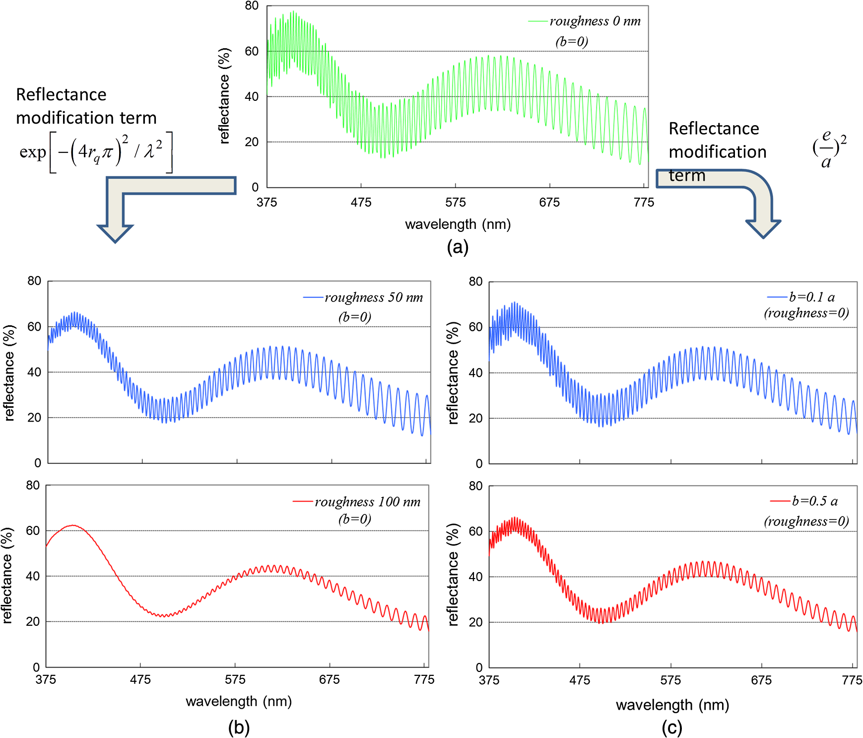 4.Accuracy Evaluation MethodologyWe utilized a calibrated standard that was built according to recommendation,27 as shown in Fig. 3, with six annular step heights certified by the National Measurement Laboratory of the Center for Measurement Standards of Taiwan (Calibration Report No. B980864). It was measured with a traceable stylus instrument according to ISO 5436-1. The nominal step heights in sequence from left to right are 5, 10, 30, 50, 75, and 100 μm. A series of tactile measurements were arranged from left to right, along the routes indicated by the arrows labeled 1, 2, 3, and 4, and the average data from all the measurements on the same ring were taken as the certified step heights, as listed in Table 1. Fig. 3Calibrated standard with six rings with nominal step heights of 5, 10, 30, 50, 75, and 100 μm in sequence from left to right. 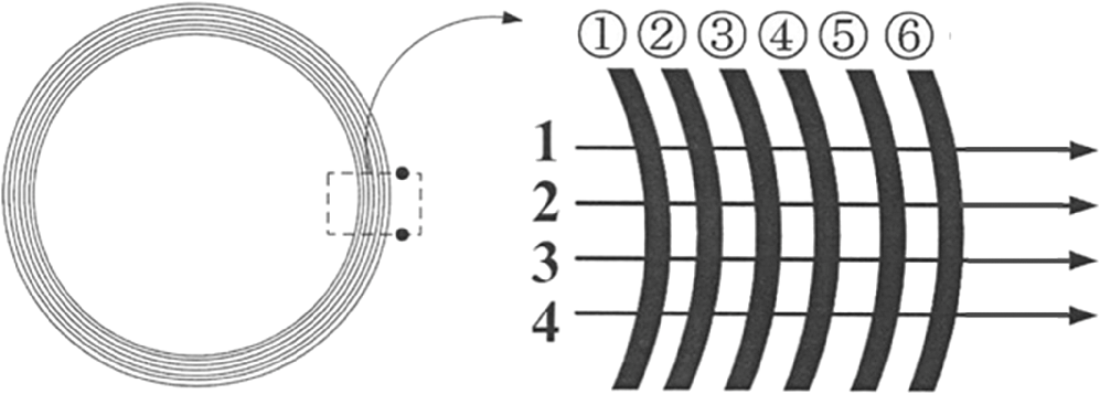 Table 1Certified step heights of calibration standard.
We used the calibrated transfer standard to evaluate the performance of refelctometer on depth measurement. The incident beam of the reflectometer was focused on the top surface of each step, so that the bottom reference plane could be considered as a relatively deep trench or bottom surface of a via. We carefully moved the illumination beam spot so that two thirds of it overlaid the bottom surface and one third of it overlaid the top surface of the stepped ring to obtain better intensity of interference spectrum. The incidence of illumination was nearly optimal for collecting as much of the intense interference spectrum as possible from the step structure. The depth measurement results, which were extracted from the interference spectrum, were used to establish the linearity over the depth range of interest. The great advantage of using normal-incidence spectral reflectometry compared to instruments that make tactile shape measurements and the cross-sectional SEM is that it is a nontactile and nondestructive method. Because of the stylus shank angle, stylus profilometers cannot measure up to the HAR TSV structure, especially with small opening CDs in the micron range. 5.Results and DiscussionsFigure 4(a) shows a top view of HDTSV array sample with circular openings. The via CD is , the via pitch is , and the aspect ratio is . The illumination spot size of covers a number of vias in a single-shot measurement. The cross-sectional SEM images shown in Figs. 4(b) and 4(c) are a wide range view and a bottom close-up view, respectively, which were used for a measurement comparison after the spectral reflectometry experiments. The via depth is , which is from a single measurement on the whole group with arrow indicating height. The via bottom is described by a half-oblate spheroid with a minor axis length of (where is the major axis length). The bottom roughness is within a range of 100 nm. Fig. 4(a) Top view of circular high-density TSV (HDTSV) sample. Via CD is , and via pitch is . (b) Wide range view and (c) a bottom close-up view, obtained by cross-sectional scanning electron microscope (SEM). The via depth is , which is from a single measurement on the whole group with arrow indicating height. The via bottom is described by a half-oblate spheroid with a minor axis length of . The bottom roughness is within a range of 100 nm. 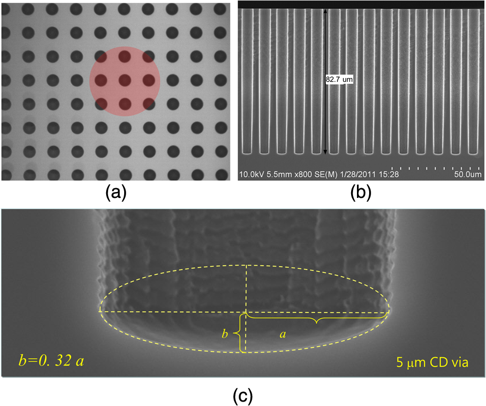 We have developed a reflectance modulation model and an inverse matching algorithm that can be used to extract the minor axis length and the bottom roughness . As shown in Fig. 2, the reflectance reacts to the bottom roughness in a manner of exponential attenuation (the shorter the wavelength range, the stronger the attenuation), but reacts to the minor axis in a uniform attenuation manner over the whole measuring wavelength range. With this physical phenomenon and a proper analysis of the inverse approach, the variations of the two correlated parameters ( and ) can be differentiated and calculated on the produced wafers. A reference library of theoretical solutions based on a bounded range of floating parameters (, ) is generated. When the reflectance spectrum is captured from a measuring sample, it is matched to the reference library to return a solution for the floating parameters. The metric of the root-mean-square error (RMSE) was used as the best match criterion, taking the root of the mean square error of a point-by-point (wavelength) comparison between the theoretical and measured data. The parameters of the modeled reflectance spectrum with the minimum RMSE are taken to be the parameters for measuring the reflectance. Figure 5 shows a theoretical model fit to the measured spectrum of the HAR HDTSV array structure shown in Fig. 4. The illuminated areas of the top silicon surface and the via opening area are roughly 81% () and 19% () of the total surface area, respectively. The via depth, , is a function of only the oscillation frequency, which is based on the phase angle difference [cos ()], as derived in Eq. (2). A preliminary fit to the experimental spectrum that only considers the frequency of the oscillation was obtained at a depth of 82.66 μm. The oscillation from the via depth is particularly obvious in the long-wavelength region, as shown magnified in the upper plot in Fig. 5. Fig. 5Experimental reflectance spectrum from HDTSV array structure shown in Fig. 4. Magnified view of oscillation in long-wavelength region is shown in upper plot. 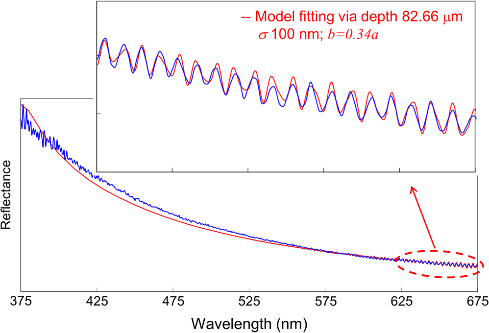 Next, the results of and were obtained through the best matching of the experimental spectrum with the reflectance modulation, by multiplying the simulated oscillation by the roughness scattering term, , and the ratio of the effective illumination term () according to Eq. (10). The best match was an effective bottom area radius of and a root-mean-square bottom roughness of 100 nm. The corresponding minor axis length, , is based on the half-oblate spheroid model of Eq. (8). The via depth resolution, , for an 82.66-μm-deep structure is considered to be 82.66 nm at 600 nm according to Eq. (7) (600 nm is approximately the average of the wavelengths for which our spectrometer is capable of resolving dense oscillations, as observed in Fig. 5). The residual errors between the measured and fit spectra can be attributed to scattering at the via sidewalls, resulting in a random variation of intensity, and are a consequence of the limitations of the model. However, the variation of reflectance intensity does not affect the extraction of parameters because the overall measured reflectance shape appears to remain close to the modeled spectra. The results of analyzing the via depth/bottom shape and roughness show good agreement between the cross-sectional SEM and the reflectometer tool. Figure 6(a) shows an experimental reflectance spectrum from an HDTSV array structure with square openings, where the nominal CD is 3 μm and the pitch is 6 μm; there is a thin oxide hard mask on top of the array, and the illumination spot is . The illuminated area of the oxide surface and the square via opening area are and 25% of the total surface area, respectively. The reflectance spectrum oscillates at two distinct frequencies—high-frequency features correspond to the deep via and low-frequency features result from the oxide hard mask. The low- and high-frequency oscillations were extracted using a spectrum-processing algorithm, as shown in Figs. 6(b) and 6(c), respectively. Curve fitting method is used for oxide layer analysis; the thickness is inferred from the best fit. Software calculates theoretical reflectance of the oxide layer, and its thickness is adjusted to achieve best fit to the measured data. An excellent model fit to the low-frequency reflectance spectra was obtained at an oxide layer thickness of 423 nm. However, dense peaks-valleys of the high-frequency oscillation make it difficult for the fitting algorithm to converge to the correct depth. The spot illuminates a large number of 3-μm CD silicon vias within dense array that might have very slightly different depths, resulting in a combination reflectance spectrum, as shown in Fig. 6(c). A variation in the spectrum amplitude that is much slower than the spectrum frequency of the reflectance itself can be observed. Here, we employ the Fourier transform (FT) algorithm, which can handle the difficult task of separating the dense peaks and valleys, as well as the combined modulation effect of the high-frequency oscillations. In addition, because the frequency of the oscillation is proportional to the via depth, it is easy to transform the reflectance spectrum to the frequency spectrum using an FT calculation. It is more reliable and practical to measure via depth larger than tens of microns using frequency analysis. Figure 6(d) shows the FT frequency spectrum that is directly calculated from the experimental data in Fig. 6(c). The results of the FT analysis reveal the via depth to be 28.51 μm. It should be noted that the single obtained frequency indicates that the depth variations among the vias within the illumination area are smaller than the resolution limit of the depth variation of 0.36 μm, as we determined in Ref. 17. There is a slight broadening on the right side of the main peak, which reveals there might be vias slightly deeper than 28.51 μm within the illumination area. Fig. 6(a) Experimental reflectance spectrum from HDTSV array structure, where nominal CD is 3 μm and pitch is 6 μm; thin oxide hard mask is present on array top; illumination spot is . (b) and (c) Low- and high-frequency oscillations extracted from reflectance in (a). (d) Fourier transform frequency spectrum calculated from experimental data in (c). 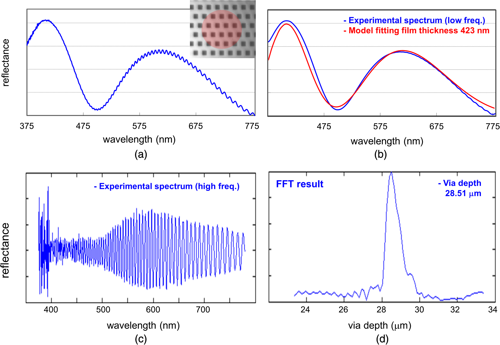 Figure 7(a) shows the best model fit results to the reflectance spectrum shown in Fig. 6(a), with an effective bottom area radius of and a root-mean-square bottom roughness of 65 nm. The corresponding minor axis length of the bottom oblate is according to the half-oblate spheroid model of Eq. (8). Figure 7(b) is a cross-sectional SEM image taken in the vicinity of the site where the reflectance spectrum was collected for measurement comparisons after the spectral reflectometry experiments; the resulting comparisons showed good agreement. Fig. 7(a) Experimental reflectance spectrum from HDTSV array structure shown in Fig. 6(a). Via CD is and via pitch is . (b) Close-up view of via bottom, obtained by cross-sectional SEM. 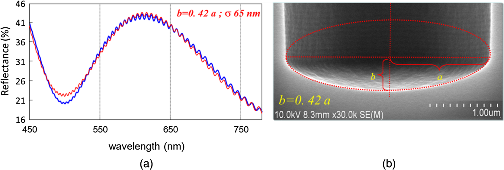 Figure 8 shows the variation of the depths of TSV arrays of nominal 5, 10, 15, 20, 25, and 30 μm CDs with the measured die-to-die as a function of position across a 200-mm-diameter test wafer. The uniformity of via depth is defined as Fig. 8Depth variation of TSV arrays measured die-to-die as a function of position across the diameter of 200-mm test wafer. 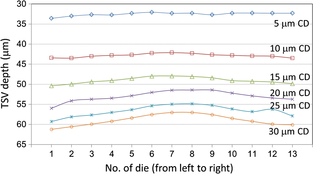 Currently developed etching process recipes have enabled efficient anisotropic etching and an etch rate . As the Si etch rate increases, the ability to control the wafer temperature becomes crucial to obtaining a uniform etch across the wafer. Thus, the TSV formation process is somewhat sensitive to via position on the wafer. Table 2 lists the via array depth uniformities for CD sizes of 5, 10, 15, 20, 25, and 30 μm, with a via-to-space ratio of for a 200-mm test wafer. The uniformities vary from 1.6 to 4.3% for different via sizes and aspect ratios. From our investigations, three factors that we can expect to affect depth uniformity are the diameters of the TSVs, the position of the die on the wafer, and the density of TSVs on the die. To achieve the best uniformity of TSV depths, spectral reflectometry, with its fast and nondestructive operation, is adopted as a useful metrology tool, allowing for in-line feedback adjustment of the process parameters that affect TSV formation. Table 2Depth uniformities of through-silicon vias within 200-mm wafer.
Figure 9 shows the reflectometer measurements being compared with calibrated values assigned to the step height structures. The plot shows a good linearity between the calibration data and the optical data within the step height range and nearly zero offset along the extrapolation. Because reflectometer and stylus tools are both inherently accurate,27 also due to large range of the measurand (5 to 100 μm) and each individual measurement discrepancy being , thus, excellent linearity and correlation are the expected results. The discrepancies are much over the step height range of 5 to 100 μm, as listed in Table 3. The step height certified values are taken from Table 1 and rounded off to two decimal places. Static measurement precision between 0.02 and 0.18 μm () was established from four quickly repeated measurements. Fig. 9Comparison of reflectometer measuring results with certified values (nominal step heights are 5, 10, 30, 50, 75, and 100 μm). 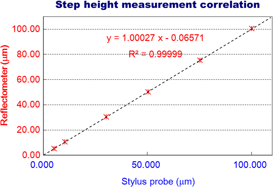 Table 3Reflectometer measurements of certified step heights of calibration standard.
Figure 10 shows the correlation between measurements with the cross-sectional SEM and the reflectometer when measuring via depths ranging from 30 to 60 μm on a 200-mm-diameter test wafer. The cross-sectional SEMs were only performed for single measurement cuts made at two sites (wafer center and edge position) owing to limitations of time and expense. The location of SEM sample cut is inside the vias array measured by reflectometer, but we could not exactly identify which via it is. Due to the large range of the measurand (30 to 60 μm) and measurement discrepancies through the range, regression of fit and linearity is excellent. Measurement precision over four repeated tests is from 0.08 to 0.24 μm () in our reflectometer experiments as listed in Table 4. The relatively greater discrepancies (compared to Table 3) might be caused by variations in the preparation of SEM samples, possibly resulting from the cross-section cleaving line not being straight, the cross-section not being perpendicular to the sample surface, and measurement inaccuracy of the SEM tool itself. Thus, the SEM measurement results, especially for the vertical depth, tend to not be repeatable, in addition to being destructive and costly. The fact that reflectometry can measure via depths nondestructively and extremely fast opens up the possibility of mapping the via depth across an entire wafer (from center to edge). Fig. 10Comparison of measurements between SEM instrument and reflectometer while measuring via depths from 30 to 60 μm. 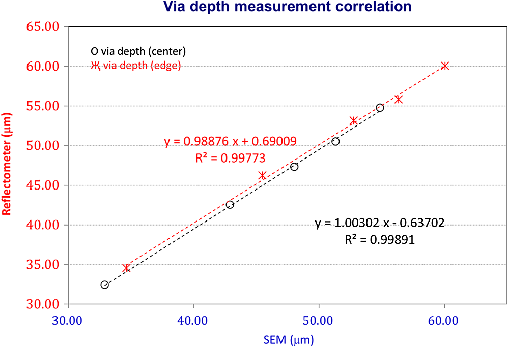 Table 4Comparison of measurements between cross-sectional scanning electron microscope and reflectometer.
6.SummaryWe demonstrated the use and enhancement of an existing wafer metrology tool, the normal-incidence spectral reflectometer, by implementing a novel theoretical model and measurement algorithm for measurements of depth, estimation of bottom shape and bottom roughness of high aspect ratio TSVs. Our nondestructive technique has measured TSV diameters as small as 3 μm and aspect ratios . Uniformity of TSV etch depth for an entire wafer can now be verified in die-to-die measurements in a nondestructive manner, allowing for instant feedback in etch process control. We have presented a methodology for testing the reflectometer-based depth measurement linearity on a calibrated step height and demonstrated excellent linearity over a range of 5 to 100 μm. The TSV depth measurement accuracy has been verified by cross-section SEM to be at the submicron level over a depth range of 30 to 60 μm, at least as linked to CDs from 5 to 30 μm. This may also be applicable to larger ranges of both CD and depth, as well as to circular and square TSV shapes, as well as other TSV layouts and densities. Our future work will focus on measurements of high-density microbumps and micropillars a few microns in diameter with varying aspect ratios. AcknowledgmentsThis work was supported by Ministry of Economic Affairs of Taiwan (Grant 100-EC-17-A-01-05-0337) and the Advanced Technology Project. The author would like to thank Kuo Cheng Huang and Weite Hsu for their contribution to the modeling and experimental work in the early development stage while they were working with the Industrial Technology Research Institute prior to the year 2011. The author also thanks Electronics and Opto-Electronics Research Laboratory for providing three-dimensional interconnect processing wafers. The author also thanks the Dimension Laboratory and National Measurement Laboratory, Taiwan, for their help with calibration of step heights. References
(2011). Google Scholar
P. de GrootX. C. de Lega,
“Valve cone measurement using white light interference microscopy in a spherical measurement geometry,”
Opt. Eng., 42
(5), 1232
–1237
(2003). http://dx.doi.org/10.1117/1.1565350 OPEGAR 0091-3286 Google Scholar
W. H. Tehet al.,
“A route towards production-worthy and non-Bosch through-silicon-via (TSV) etch, TSV metrology, and TSV integration,”
in Proc. of the IEEE Int. Conf. on 3D System Integration,
(2009). Google Scholar
M. Knowles,
“Optical metrology for TSV process control,”
(2014) February ). 2014). Google Scholar
D. Marxet al.,
“Wafer thickness sensor (WTS) for etched depth measurement of TSV,”
in Proc. of the Int. Wafer-Level Packaging Conf.,
(2009). Google Scholar
H. Takizawa,
“Development of TSV etching depth measurement systems,”
in 6th Annual SEMATECH Symp.,
(2010). Google Scholar
P. K. SchenckD. L. KaiserA. V. Davydov,
“High throughput characterization of the optical properties of compositionally graded combinatorial films,”
Appl. Surf. Sci., 223
(1–3), 200
–205
(2004). http://dx.doi.org/10.1016/j.apsusc.2003.07.005 ASUSEE 0169-4332 Google Scholar
Y. Fenget al.,
“OCD study of critical dimension and line-shape control of shallow-trench-isolation structures,”
Proc. SPIE, 5375 1173
–1182
(2004). http://dx.doi.org/10.1117/12.536582 PSISDG 0277-786X Google Scholar
H. T. HuangF. L. Terry Jr.,
“Spectroscopic ellipsometry and reflectometry from gratings (scatterometry) for critical dimension measurement and in situ, real-time process monitoring,”
Thin Solid Films, 455–456 828
–836
(2004). http://dx.doi.org/10.1016/j.tsf.2004.04.010 THSFAP 0040-6090 Google Scholar
Z. Liuet al.,
“Measurement of deep silicon trench profile using normal incidence optical CD metrology,”
Proc. SPIE, 5752 1152
–1160
(2005). http://dx.doi.org/10.1117/12.600121 PSISDG 0277-786X Google Scholar
C. A. Duranet al.,
“Infrared reflectometry for metrology of trenches in power devices,”
in IEEE/SEMI Advanced Semiconductor Manufacturing Conf.,
175
(2007). Google Scholar
M. Horieet al.,
“UV-reflectometry for fast trench-depth measurement,”
Proc. SPIE, 6922 69223D
(2008). http://dx.doi.org/10.1117/12.772425 PSISDG 0277-786X Google Scholar
Y. S. KuF. S. Yang,
“Reflectometer-based metrology for high-aspect ratio via measurement,”
Opt. Express, 18
(7), 7269
–7280
(2010). http://dx.doi.org/10.1364/OE.18.007269 OPEXFF 1094-4087 Google Scholar
Y. S. KuK. C. HuangW. Hsu,
“Characterization of high density through silicon vias with spectral reflectometry,”
Opt. Express, 19
(7), 5993
–6006
(2011). http://dx.doi.org/10.1364/OE.19.005993 OPEXFF 1094-4087 Google Scholar
H. SinghC. RusuV. Vahedi,
“Etch challenges for 3-D integration,”
in 3rd Workshop on Plasma Etch and Strip in Microelectronics,
(2010). Google Scholar
M. Puechet al.,
“Fabrication of 3D packaging TSV using DRIE,”
in Symp. on Design, Test, Integration and Packaging of MEMS/MOEMS,
(2008). Google Scholar
F. Liuet al.,
“A 300-mm wafer-level three-dimensional integration scheme using tungsten through-silicon via and hybrid Cu-adhesive bonding,”
in Proc. of the IEEE Int. Electron Devices Meeting,
599
(2008). Google Scholar
M. PuechJ. M. ThevenoudJ. M. Gruffat,
“DRIE for MEMS devices,”
Adv. Packag., 17
(3), 25
(2008). Google Scholar
(2009). Google Scholar
J. Sumaya-MartinezO. Mata-MendezF. Chavez-Rivas,
“Rigorous theory of the diffraction of Gaussian beams by finite gratings: TE polarization,”
J. Opt. Soc. Am. A, 20
(5), 827
–835
(2003). http://dx.doi.org/10.1364/JOSAA.20.000827 JOAOD6 0740-3232 Google Scholar
H. E. BennettJ. O. Porteus,
“Relation between surface roughness and specular reflectance at normal incidence,”
J. Opt. Soc. Am., 51
(2), 123
–129
(1961). http://dx.doi.org/10.1364/JOSA.51.000123 JOSAAH 0030-3941 Google Scholar
M. Basset al., Handbook of Optics, 3rd ed.McGraw-Hill, USA
(2009). Google Scholar
K. C. Huang,
“The study of high aspect ratio TSV metrology,”
National Tsing Hua University,
(2010). Google Scholar
L. Koenders,
“WGDM-7: preliminary comparison on nanometrology according to the rules of CCL key comparisons, Nano2: step height standards,”
(2003). Google Scholar
BiographyYi-Sha Ku received a BS in physics in 1985 from National Central University and a PhD in nuclear science from National Tsing Hua University, Taiwan, in 1992. She is currently a senior principal researcher at ITRI and a professor at National Tsing Hua University. Previously, she worked with National Measurement Laboratory for 11 years and was responsible for the development of primary quantum metrology standards. She has 10 years of experience in the field of overlay metrology and was engaged in model-based method and analysis algorithms, in particular. Her current research interests are developing metrology solutions for three-dimensional interconnect processes. |
||||||||||||||||||||||||||||||||||||||||||||||||||||||||||||||||||||||||||||||||||||||||||||||||||||||||||||||||||||||||||||||||||||||||||||||||||||||||||||||||||||||


