
|
|
1.IntroductionMask, process, and lithography-tool parameters are the most important aspects for achieving high lithography performance. Various methods have been proposed to optimize these parameters in recent years. Optical proximity correction is the main technology to optimize the mask pattern to enhance the resolution.1 Source mask optimization (SMO) improves the lithography performance by co-optimizing the illumination source and mask.2 The optimized mask structure and source shape via SMO suffers from extreme complexity, especially for the pixelated mask and source,3–5 which leads to difficulty in manufacturing. Furthermore, the parameters related to the process, such as the film stacks, postexposure bake (PEB), and photoresist development, have a strong impact on the process window (PW).6,7 However, most published optimization technologies were implemented under fixed process conditions.3,8,9 Moreover, lithography-tool parameters such as the numerical aperture (NA) and source parameter also determine the PW.1 Actually, the parameters related to the mask, process, and lithography tool simultaneously impact the lithography performance.10,11 The lithography effects caused by multiple parameter errors could compensate for each other,12 indicating that the co-optimization of multiple parameters could improve the PW. However, no effective methods have been published for co-optimizing the mask, process, and lithography-tool parameters. In this study, the first time to our knowledge, a co-optimization method is developed to simultaneously optimize the mask, process, and lithography-tool parameters. The PW is extended by co-optimizing the parameters rather than optimizing them independently. An effective co-optimization flow is built to realize this goal. Conjugate gradient algorithm is used to calculate the search direction in optimization. The parameters are optimized along the search direction, where a line search is applied within the parameters’ boundary. Mask, process, and lithography-tool parameter co-optimization (MPLCO) is a multidimensional optimization method. As large-scale parameters are obstructed by small-scale parameters during co-optimization, we also propose a normalized conjugate gradient (NCG) algorithm to improve the convergence efficiency of the MPLCO. In order to reduce the complexity of the mask and source, a parametric mask and source are used in the MPLCO. The mask pattern is optimized by adding bias and changing the feature transmittance, while the source shape is optimized by only adjusting the sigma value in the MPLCO. As an example, we chose eight parameters in the MPLCO to optimize 45-nm node patterns. The MPLCO results show that the depth of focus (DOF) of the line-space pattern is 93.75% larger than only mask and source are optimized. At the same time, the complexity of the mask and source has been reduced compared with pixelated SMO in Ref. 3. In order to further improve the PW of the SMO work in Ref. 3, we optimize the process parameters of the SMO. The DOF of the SMO with optimized process parameters is 13.54% larger than the SMO for the line-space pattern but still smaller than that of MPLCO. The co-optimization results demonstrate that the large PW could be obtained only if the mask, process, and lithography-tool parameters are optimized simultaneously. The remainder of the paper is organized as follows. In Sec. 2, the MPLCO is described in detail. The optimization results are presented in Sec. 3. Finally, the conclusions are summarized in Sec. 4. 2.Co-Optimization MethodThe goal of MPLCO is to achieve high lithography performance in a large PW. To realize this goal, we first create an effective cost function to evaluate the lithography performance. The cost function is sufficient in promoting the optimization of the PW and benefits to the optimization procedure. Then, the parameters are optimized along the search direction iteratively until the largest PW is found. 2.1.Cost FunctionThe cost function is composed of the DOF, image contrast, and normalized image log-slope (NILS). Usually, the PW is measured under a designated metrology plane, where the metrology plane is a slice through the aerial image or photoresist pattern to make the measurement. The overlap of PW (common PW) through various metrology planes could evaluate the overall lithography performance. A common method for evaluating the overlap PW is to examine the DOF with specific exposure latitude (EL), and a larger DOF indicates better lithography performance.11,13 Thus, the DOF is chosen as the main objective function in the optimization. The DOF is a highly nonlinear function; it is usually been trapped at a local minimum when using a gradient-based algorithm.14,15 Some other objective functions should be used to assist in optimizing the DOF. Because the image contrast and NILS are strongly related to the DOF14,16–18 and converge much easier than DOF, they can serve as the assistant objective function in promoting the optimization of the DOF. Therefore, the cost function is formulated as a superposition of the objective functions mentioned above by assigning different weights. where , , and represent the value of the aerial image contrast, the NILS, and the DOF with different ELs, respectively; , , and are the corresponding weights of the objective functions, respectively; represents the ’th EL value; is the ’th metrology plane.The cost function is beneficial to optimizing the PW, while the image contrast and NILS are used to promote the optimization of the DOF. Thus, the weight should be set much larger than and in optimization. PROLITH software is used to simulate the DOF, contrast, and NILS owing to its superior ability in lithography simulation, where the mask, process, and lithography-tool models are accurately established. 2.2.Co-Optimization FlowIn this section, the parametric-based MPLCO is proposed and realized by an NCG algorithm. First, all parameters in the optimization are normalized in the same scale. Then, the parameters are optimized along the search direction iteratively until the best combination of mask, process, and lithography-tool parameters is found. Because the combination of mask, process, and lithography-tool parameters is a multidimensional point in the optimization space, we use point instead of combination and use to denote each parameter in the following sections. The co-optimization flow can be generalized in the following steps, as shown in Fig. 1.
It is noted that a restitution operation (an inverse operation of normalization) is necessary for the simulation of when calculating the search direction (step 3) and applying the line search (step 5). All parameters need to be restituted to their original scales for the PROLITH simulation of DOF, contrast, and NILS. Without the parameter normalization step (step 2) and the restitution operation, the optimization procedure can be denoted as a conventional conjugate gradient (CCG) method. The NCG method is developed on the basis of the CCG method and is an improvement of the CCG method. The normalizing operation could greatly improve the convergence when optimizing different-scale parameters, and the advantage is demonstrated in Sec. 3.2. Fig. 1Co-optimization flow. All the parameters are normalized into the same scale in optimization and should be restitute to their original scales for PROLITH simulation in step 3 and step 5. 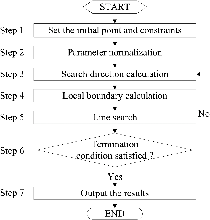 Fig. 2Illustration of the global boundary and local boundary. and are the global boundaries of the two parameters and , which have been set in step 1, while and are the local boundaries along the search direction . 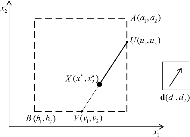 The MPLCO is a multidimensional optimization method; thus, all parameters related to the mask, process, and lithography tool could be optimized simultaneously. The convergence robustness of the MPLCO is guaranteed in three aspects. First, the cost function we built is easy to converge. As the DOF is easily trapped at the local minimum, we add the image contrast and NILS as assistant objective function. Second, the normalization in MPLCO guarantees the optimization of different scale parameters. Third, the Hopfinger golden section search method used in MPLCO is able to solve the nonunimodal cost function. 3.Co-Optimization Results3.1.Simulation ConditionsTwo typical geometries of a 45-nm node are used to demonstrate the validity of the MPLCO: the semidense line-space pattern and the dense contact hole. The duty ratios of these patterns are 1:2 and 1:1. The critical dimension (CD) of the line is 45 nm, while the CD of the contact hole is 60 nm.3 The PROLITH programming interface helps to communicate between the optimization algorithm and PROLITH.25 The PROLITH simulation condition is same as that in Ref. 3 except that the parameters have been optimized. We use a water () immersion lithography system with the demagnification factor . The source shape is annular with a fixed sigma width . The illumination is Y-polarized for the line-space pattern and TE-polarized for the contact hole.3 Since a tunable transmittance mask is available, the feature transmittance could be varied over a large range,26 and an attenuated phase-shift mask is used to enhance the lithography capability. The well-calibrated photoresist JSR ARX2895JN is used with a thickness of 120 nm for the line-space pattern and 102 nm for the contact hole.3 Dual bottom antireflective coatings (BARCs) are applied to reduce the substrate reflectivity and are optimized under the initial parameter settings. The thicknesses of BARCs are 33 and 43 nm for the line-space pattern and 24 and 43 nm for contact hole. The PW is constrained by the tolerances of , an 80-deg sidewall angle, and a 10% photoresist loss to maintain pattern fidelity.27 It is necessary to use a robust photoresist model to optimize the process parameters. In order to accurately simulate the process conditions, a full physical photoresist model, three-stage PEB model, and Mack development model are used in PROLITH.25 The full physical photoresist model is capable of simulating the reaction and diffusion of a chemically amplified photoresist accurately. The three-stage PEB model describes the temperature variation when the wafer is placed on a hotplate or chillplate and the wafer transition time between the two plates.6 The three-stage temperature profile is represented by nine parameters: the bake temperature, the bake duration, and the temperature rise (or fall) time for each stage. The initial temperature is 25°C. The temperatures for the hotplate stage, transfer stage, and chillplate stage are 110, 45, and 25°C, respectively. The rise (or fall) times for these three stages are 5, 50, and 5 s, respectively.25 Eight parameters including the mask, process, and lithography-tool parameters are selected as an example to demonstrate the validity of the MPLCO. For the mask parameters, the mask bias and feature transmittance are optimized. For the process parameters, the hotplate duration, transition duration, chillplate duration, and photoresist development time are chosen for the optimization. For the lithography-tool parameters, the outer sigma of annular illumination and the NA are selected for the optimization. The DOF at is chosen to evaluate the PW, where is a common value for 45-nm lithography and is closer to the actual case.10 The goal of co-optimization is to extend the DOF at to be as large as possible. The DOF at is another objective function in the optimization. The weights for , , , and in are , , , and , respectively. Only one metrology plane is set for each pattern, and the metrology plane could cover a whole pitch. The PWs measured at the metrology planes are the overlap PWs for these two infinite and periodic patterns. The metrology plane for the line space is a cutline perpendicular to the line direction, while for the contact hole the cutline is set at the center of the hole. The optimization terminates after 20 iterations of the line search. The unoptimized parameters for the line space and contact hole are set as the initial point . The ranges of the parameters are set in a reasonable range, which ensures that the values of the parameters are realizable in lithography. The conditions for the initial value , the minimum value (lower global boundary), the maximum value (upper global boundary), and the increment of the parameters are listed in Table 1. Owing to the different properties of these parameters, different increments and are set to calculate the gradient for the CCG and NCG methods. It is noted that is the actual value of the parameter, while is the normalized value. Table 1Co-optimization conditions and results.
Note: CCG, conventional conjugate gradient, NCG, normalized conjugate gradient, MPLCO, mask, process, and lithography-tool parameter co-optimization. 3.2.Co-Optimization ResultsThe results are demonstrated in two aspects. We first present the improvement in the PW by using the MPLCO method. The convergence efficiency of the MPLCO by using the CCG (MPLCO-CCG) method and the proposed NCG (MPLCO-NCG) method are also compared. Then, the mask and source complexities are compared between the MPLCO method and the pixelated SMO in Ref. 3. The optimized parameters of the MPLCO-CCG and MPLCO-NCG methods are listed in the last two columns in Table 1. The MPLCO-CCG results show no changes for the mask bias, PEB duration, and develop time, although the small-scale parameters are well optimized. This is mainly due to the drawback of the local boundary calculation when optimizing the different scale parameters. The optimization of the large-scale parameters is limited by small-scale parameters in the optimization procedure. However, when all the parameters are normalized to the same scale in the MPLCO-NCG method, the optimization can move further. The normalized method could improve the convergence efficiency of the optimization. Figure 3 illustrates the convergence curve of the MPLCO-CCG and MPLCO-NCG methods, which show that the MPLCO-NCG method could effectively reduce the cost function. Fig. 3Convergence curves of the mask, process, and lithography-tool parameter co-optimization–conventional conjugate gradient (MPLCO-CCG) and MPLCO–normalized conjugate gradient (NCG) methods for the (a) line space and (b) contact hole. The cost function could be effectively reduced after the parameters have been normalized when using the MPLCO-NCG method. 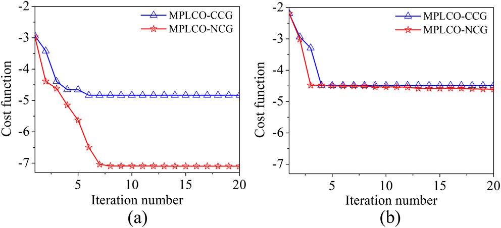 The MPLCO-NCG method greatly decreases the hotplate and chillplate duration but increases the development time. The PEB mainly affects the reaction of chemically amplified photoresist, which thereby impacts the profile of the photoresist. The entire PEB durations are 29.96 and 99.67 s for the line-space pattern and contact hole, which are shorter than the initial setting of 100 s. The development time affects the CD of the photoresist, which has been optimized to 60 and 24.37 s for the line-space pattern and contact hole. The optimized process parameters ensure the exact chemical reaction of the photoresist with an acceptable profile in a large PW. The EL versus DOF curves for the line-space pattern and contact hole are illustrated in Fig. 4. The curves denoted with triangles and stars represent the PW of the MPLCO-CCG and MPLCO-NCG methods, respectively. We use the dashed line to indicate the DOF at in the figure. The DOF at of the MPLCO-CCG and MPLCO-NCG methods are 0.349 and 0.558 μm for the line-space pattern, respectively, and 0.344 and 0.356 μm for the contact hole, respectively. The PW is greatly extended after co-optimization, especially when the mask, process, and lithography-tool parameters are well optimized by using the MPLCO-NCG method. The DOF at of the MPLCO-NCG method increases by 59.89 and 3.49% for the line-space pattern and contact hole compared with the MPLCO-CCG method. The reason is mainly because the large-scale parameters are not being optimized when using the MPLCO-CCG. The comparison between MPLCO-CCG and MPLCO-NCG indicates that the more parameters have been well optimized, the larger PW can be obtained. As an SMO work is done to extending the PW in Ref. 3, the EL versus DOF curve of the SMO denoted with square is represented in Fig. 4. The DOF at of the SMO is 0.288 μm for line-space pattern and 0.172 μm for contact hole, which are much smaller than the DOF of MPLCO-NCG. The comparison between the MPLCO and SMO could also prove that large PW can be obtained when more parameters are involved in optimization. Fig. 4Exposure latitude (EL) versus depth of focus (DOF) comparison for the (a) line space and (b) contact hole. The process window (PW) is greatly extended when the mask, process, and lithography-tool parameters are well optimized simultaneously by using the MPLCO-NCG method. The PW of source mask optimization (SMO) with optimized process condition is larger than that of SMO, but smaller than MPLCO-NCG. 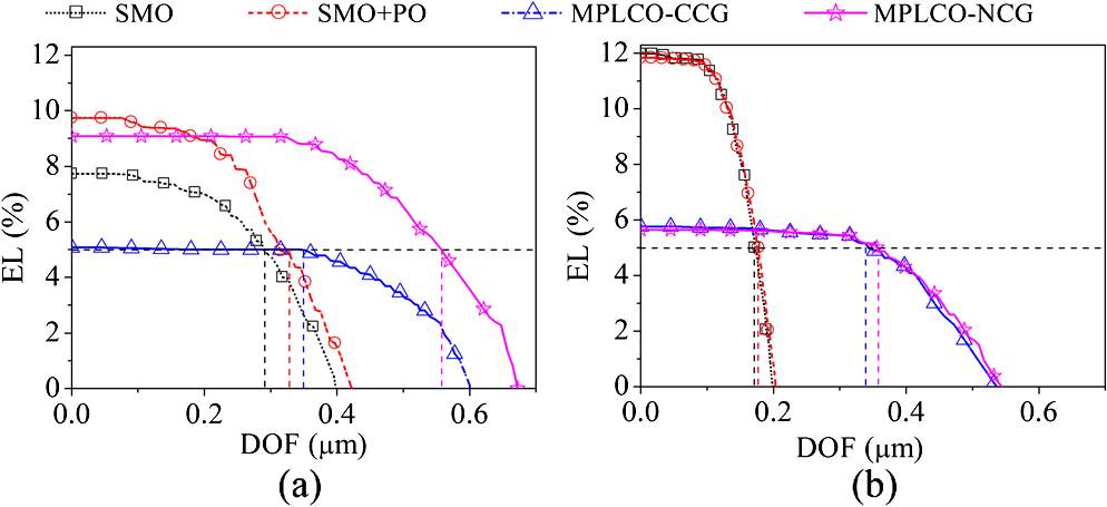 In order to demonstrate the merits of MPLCO and the impact of the process parameters on lithography, we only optimize the process parameters under the condition that the mask and source are optimized by the SMO in Ref. 3. The increments of NCG method are for the line-space pattern and for the contact hole. The parameter settings and optimized results are listed in Table 2. The EL versus DOF curves are shown in Fig. 4. The DOF at of the SMO with process optimization (PO) are 0.327 μm for the line-space pattern and 0.178 μm for the contact hole, which are 13.54 and 3.49% larger than that of SMO. This verifies that the PW could be extended by optimizing the process parameters. From Fig. 4, we also find that the DOF at for the MPLCO-NCG method is still larger than that of SMO with PO. Although the maximum EL of the MPLCO-NCG method is smaller than that of SMO and SMO with PO, the DOF at of the MPLCO-NCG method definitely increases. The results indicate that a large PW could be obtained only if the mask, process, and lithography-tool parameters are optimized simultaneously. Table 2Co-optimization of the process parameters for source mask optimization.
The second advantage of the proposed MPLCO method is to reduce the mask and source complexity. A parametric mask and source are used in the MPLCO. For comparison, Fig. 5 shows the mask pattern and source shape of the SMO, MPLCO-CCG method, and MPLCO-NCG method. For the contact hole of the SMO, the mask pattern is much more complex compared with the MPLCO-CCG and MPLCO-NCG results. A complex mask is difficult to manufacture and will greatly increase the cost of mask fabrication. For the parametric mask, the mask pattern has only been biased rather than applying complex mask correction, which could reduce the complexity of the mask. The source shapes of the SMO results suffer from an intricate distribution with a nonuniform intensity. It is necessary to use a customized diffractive optical element or an expensive programmable illuminator to generate the pixelated source. However, one just needs to adjust the sigma value for the parametric source in which the source shape always has high uniformity and stability. Fig. 5Comparison of the optimized mask pattern and source shape among the SMO, MPLCO-CCG, and MPLCO-NCG results. The parametric mask and source optimized by MPLCO-CCG and MPLCO-NCG suffers less complexity compared with pixelate SMO. 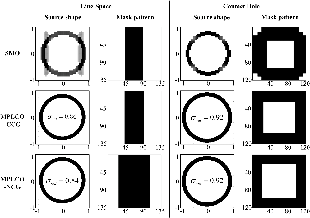 The mask error enhancement factor (MEEF) is compared. The MEEF of the SMO result, MPLCO-CCG result, and MPLCO-NCG result are 5.45, 4.74, and 4.47 for the line-space pattern, respectively, and 12.69, 15, and 15.39 for the contact hole, respectively. There are nearly no improvements for the MEEF when using MPLCO compared with SMO. The MEEF of MPLCO result is smaller than SMO result for line-space pattern, but larger than SMO result for contact hole. Contact hole suffers the largest MEEFs of any feature type because the change in mask size of a regular contact hole will lead to change in exposure dose.27 There are more clear areas at the corner of contact hole optimized by SMO; the change of mask size will lead to less change in exposure dose compared with the regular contact hole optimized by MPLCO. Therefore, the MEEF of regular contact hole optimized by MPLCO is larger than the contact hole optimized by SMO. 4.Conclusion and DiscussionThis paper proposes an MPLCO method that can optimize the mask, process, and lithography-tool parameters simultaneously. An NCG algorithm is used in the MPLCO to improve the convergence efficiency and is successfully applied to optimize different scale parameters. As the process parameters have strong impact on lithography performance, it is necessary to use a full physical photoresist model to simulate the process behavior accurately when optimizing the process parameters. The PW of the SMO with optimized process is larger than the SMO, but still smaller than that of MPLCO. The results indicate that the more parameters have been optimized simultaneously, the larger PW could be obtained. In addition, the complexity of the mask and source could be greatly reduced by using the MPLCO compared with the SMO. The mask pattern has only been biased rather than applying complex mask correction, while the source shape is controlled by adjusting the sigma value. The assumption and simplification for the mask is sufficient when optimizing the one-dimensional line-space pattern and two-dimensional contact hole. The cost of fabrication could be greatly reduced by using the parametric mask and source. In our future work, we will model the complex two-dimensional mask pattern in parametric form and apply the MPLCO to it. AcknowledgmentsWe gratefully acknowledge the financial support from the National Science and Technology Major Project, Key Program of National Natural Science Foundation of China under Grant No. 60938003, and National Natural Science Foundation of China under Grant No. 61204113. This work is also supported by the Key Laboratory of Photoelectronic Imaging Technology and System, Beijing Institute of Technology, Ministry of Education of China, under Grant No. 2013OEIOF05. We thank KLA-Tencor Corporation for providing academic use of PROLITH. ReferencesA. K. Wong, Resolution Enhancement Techniques in Optical Lithography, SPIE, Bellingham, WA
(2001). Google Scholar
X. MaG. R. Arce, Computational Lithography, 1st ed.John Wiley and Sons, New York
(2010). Google Scholar
X. Maet al.,
“Hybrid source mask optimization for robust immersion lithography,”
Appl. Opt., 52
(18), 4200
–4211
(2013). http://dx.doi.org/10.1364/AO.52.004200 APOPAI 0003-6935 Google Scholar
J. LiY. ShenE. Y. Lam,
“Hotspot-aware fast source and mask optimization,”
Opt. Express, 20
(19), 21792
–21804
(2012). http://dx.doi.org/10.1364/OE.20.021792 OPEXFF 1094-4087 Google Scholar
X. MaG. R. Arce,
“Pixel-based simultaneous source and mask optimization for resolution enhancement in optical lithography,”
Opt. Express, 17
(7), 5783
–5793
(2009). http://dx.doi.org/10.1364/OE.17.005783 OPEXFF 1094-4087 Google Scholar
M. D. SmithC. MackJ. S. Pertersen,
“Modeling the impact of thermal history during post exposure bake on the lithographic performance of chemically amplified resists,”
Proc. SPIE, 4345 1013
–1021
(2001). http://dx.doi.org/10.1117/12.436826 PSISDG 0277-786X Google Scholar
B. M. Rathsacket al.,
“Optical lithography simulation and photoresist optimization for photomask fabrication,”
Proc. SPIE, 3678 1215
–1226
(1999). http://dx.doi.org/10.1117/12.350173 PSISDG 0277-786X Google Scholar
Y. Shenet al.,
“Robust level-set-based inverse lithography,”
Opt. Express, 19
(6), 5511
–5521
(2011). http://dx.doi.org/10.1364/OE.19.005511 OPEXFF 1094-4087 Google Scholar
P. YuS. X. ShiD. Z. Pan,
“True process variation aware optical proximity correction with variational lithography modeling and model calibration,”
J. Micro/Nanolith. MEMS MOEMS, 6
(3), 031004
(2007). http://dx.doi.org/10.1117/1.2752814 JMMMGF 1932-5134 Google Scholar
A. V. Pretet al.,
“Combined mask and illumination scheme optimization for robust contact patterning on 45 nm technology node flash memory devices,”
Proc. SPIE, 6924 69243B
(2008). http://dx.doi.org/10.1117/12.772676 PSISDG 0277-786X Google Scholar
J. V. Wingerdenet al.,
“Lithographic process optimization using process capability analysis,”
Proc. SPIE, 5040 882
–893
(2003). http://dx.doi.org/10.1117/12.485520 PSISDG 0277-786X Google Scholar
Y. Liet al.,
“The cross talk of multi-errors impact on lithography performance and the method of its control,”
Proc. SPIE, 8418 841802
(2012). http://dx.doi.org/10.1117/12.978295 PSISDG 0277-786X Google Scholar
N. JiaE. Y. Lam,
“Pixelated source mask optimization for process robustness in optical lithography,”
Opt. Express, 19
(20), 19384
–19398
(2011). http://dx.doi.org/10.1364/OE.19.019384 OPEXFF 1094-4087 Google Scholar
Y. Granik,
“Source optimization for image fidelity and throughput,”
J. Microlithogr., Microfabr., Microsyst., 3
(4), 509
–522
(2004). http://dx.doi.org/10.1117/1.1794708 Google Scholar
A. E. RosenbluthN. Seong,
“Global optimization of the illumination distribution to maximize integrated process window,”
Proc. SPIE, 6154 61540H
(2006). http://dx.doi.org/10.1117/12.656950 PSISDG 0277-786X Google Scholar
J. A. TorresY. GranikF. Schellenberg,
“Contrast analysis and optimization for resolution enhancement technique,”
J. Microlithogr., Microfabr., Microsyst., 2
(2), 119
–128
(2003). http://dx.doi.org/10.1117/1.1562931 Google Scholar
J. YuP. Yu,
“Impacts of cost functions on inverse lithography patterning,”
Opt. Express, 18
(22), 23331
–23342
(2010). http://dx.doi.org/10.1364/OE.18.023331 OPEXFF 1094-4087 Google Scholar
M. C. SmaylingV. Axelrad,
“32 nm and below logic patterning using optimized illumination and double patterning,”
Proc. SPIE, 7274 72740K
(2009). http://dx.doi.org/10.1117/12.814258 PSISDG 0277-786X Google Scholar
J. YuP. YuH. Chao,
“Fast source optimization involving quadratic line-contour objectives for the resist image,”
Opt. Express, 20
(7), 8161
–8174
(2012). http://dx.doi.org/10.1364/OE.20.008161 OPEXFF 1094-4087 Google Scholar
A. PoonawalaP. Milanfar,
“Mask design for optical microlithography—an inverse imaging problem,”
IEEE Trans. Image Process., 16
(3), 774
–788
(2007). http://dx.doi.org/10.1109/TIP.2006.891332 IIPRE4 1057-7149 Google Scholar
Y. Granik,
“Fast pixel-based mask optimization for inverse lithography,”
J. Microlithogr., Microfabr., Microsyst., 5
(4), 043002
(2006). http://dx.doi.org/10.1117/1.2399537 Google Scholar
Y. Peng,
“Gradient-based source and mask optimization in optical lithography,”
IEEE Trans. Image Process., 20
(10), 2856
–2864
(2011). http://dx.doi.org/10.1109/TIP.2011.2131668 IIPRE4 1057-7149 Google Scholar
A. RavindranK. M. RagsdellG. V. Reklaitis, Engineering Optimization Methods and Applications, John Wiley and Sons, New Jersey
(2006). Google Scholar
E. Hopfinger,
“On the solution of the unidimensional local minimization problem,”
J. Optim. Theory Appl., 18
(3), 425
–428
(1976). http://dx.doi.org/10.1007/BF00933821 JOTABN 0022-3239 Google Scholar
B. S. Kasprowiczet al.,
“Tunable transmission phase mask options for node gate and contact processing,”
Proc. SPIE, 5754 1469
–1477
(2005). http://dx.doi.org/10.1117/12.601011 PSISDG 0277-786X Google Scholar
C. Mack, Fundamental Principles of Optical Lithography: The Science of Microfabrication, John Wiley and Sons, New York
(2007). Google Scholar
BiographyXuejia Guo received his BS degree in optical information science and technology from University of Jinan in 2008. He is currently a PhD candidate directed by Professor Yanqiu Li in the School of Optoelectronics at Beijing Institute of Technology. His current interests involve lithography simulation and optimization. Yanqiu Li received her MS and PhD degrees in optics from Harbin Institute of Technology of China. She is currently a professor of School of Optoelectronics at Beijing Institute of Technology, Beijing, China. She holds over 30 Chinese patents and has published numerous articles on lithographic science. Lisong Dong received his BS degree in applied physics from Hefei University of Technology, China, in 2008. He is currently a PhD candidate directed by Professor Yanqiu Li at Beijing Institute of Technology, Beijing, China. His research interests include lithography simulation and resolution enhancement technology. Lihui Liu received his BS and MS degrees in optics from Hebei University, respectively, in 1999 and 2002. He received his PhD from Institute of Modern Optics in NanKai University in 2005. He is currently an associate professor of School of Optoelectronics at Beijing Institute of Technology, Beijing, China. His research is focused on optical sensing, lithography simulation, and optimization. |
||||||||||||||||||||||||||||||||||||||||||||||||||||||||||||||||||||||||||||||||||||||||||||||||||||||||||||||||||||||||||||||||||||||||||||||||||||||||||||||||||||||||||||||||||||||


