|
|
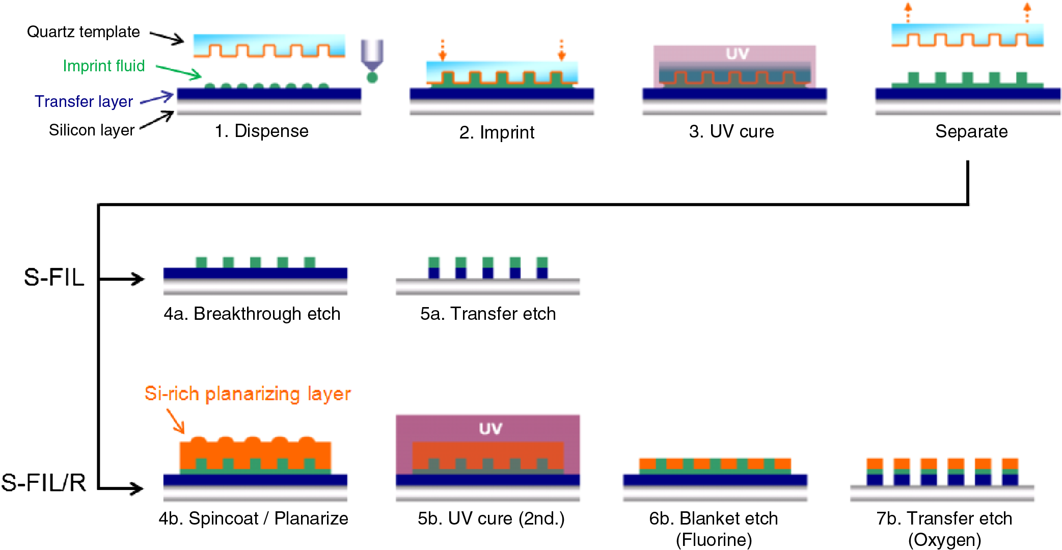
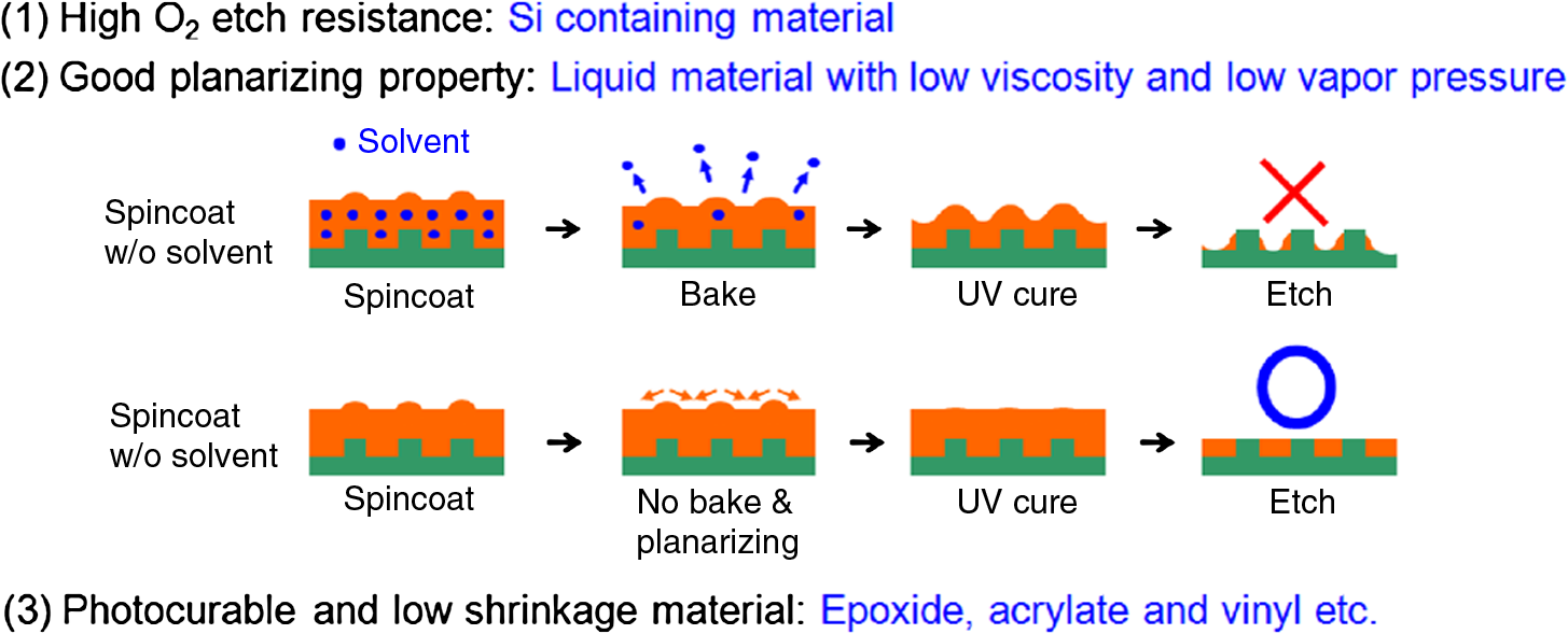
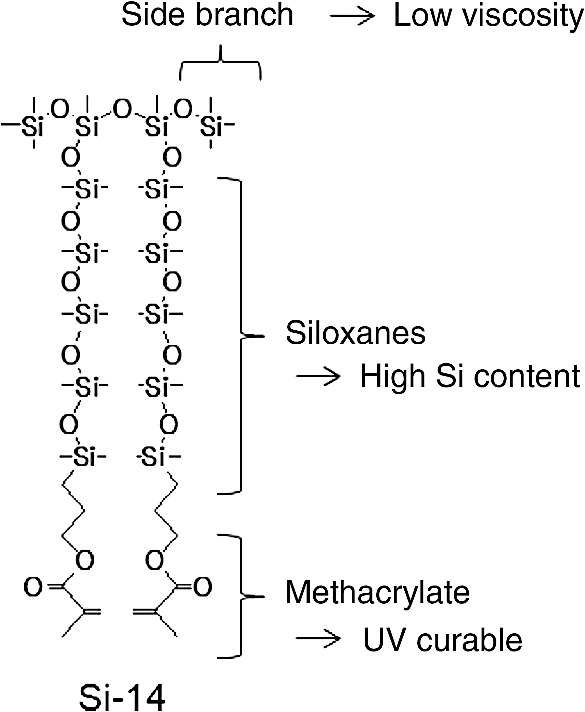
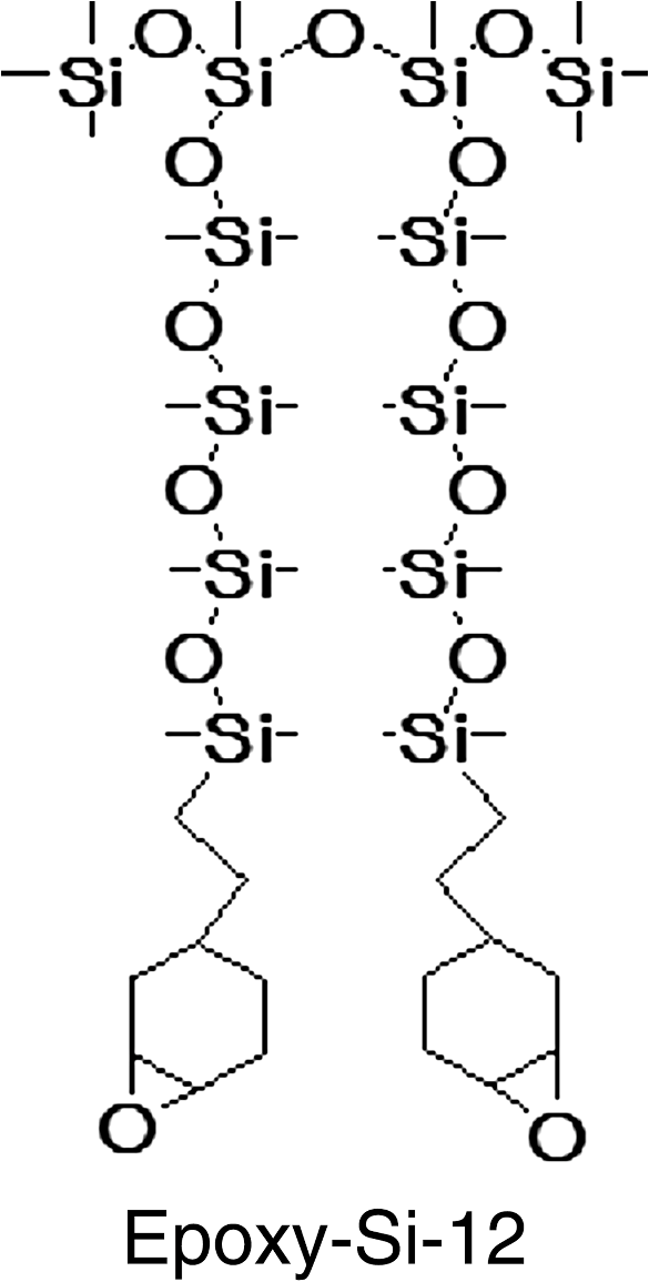
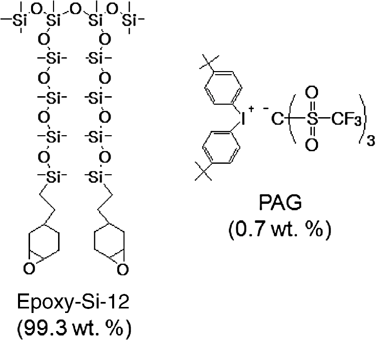
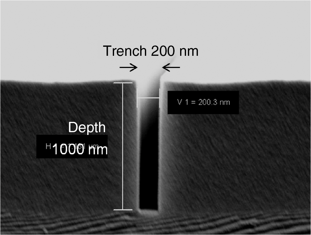
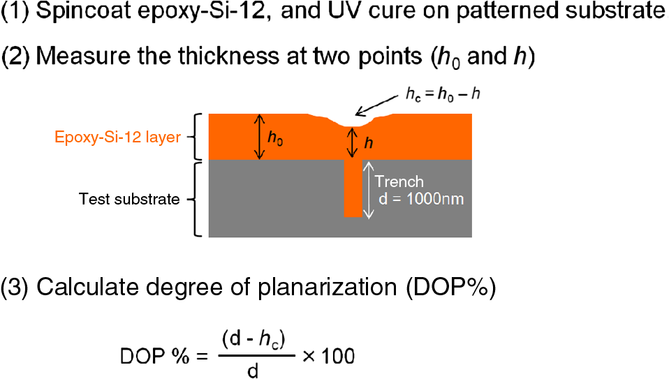
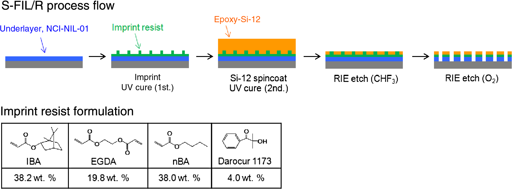
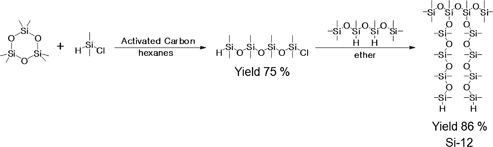
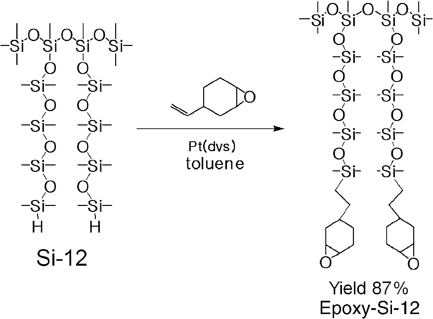
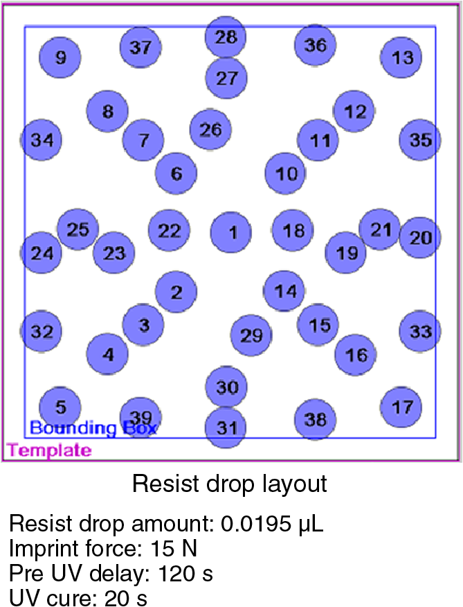
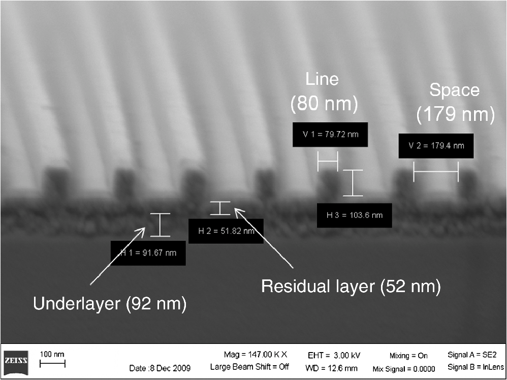
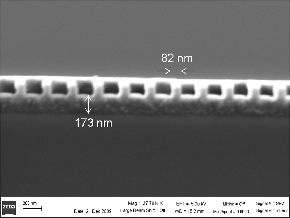
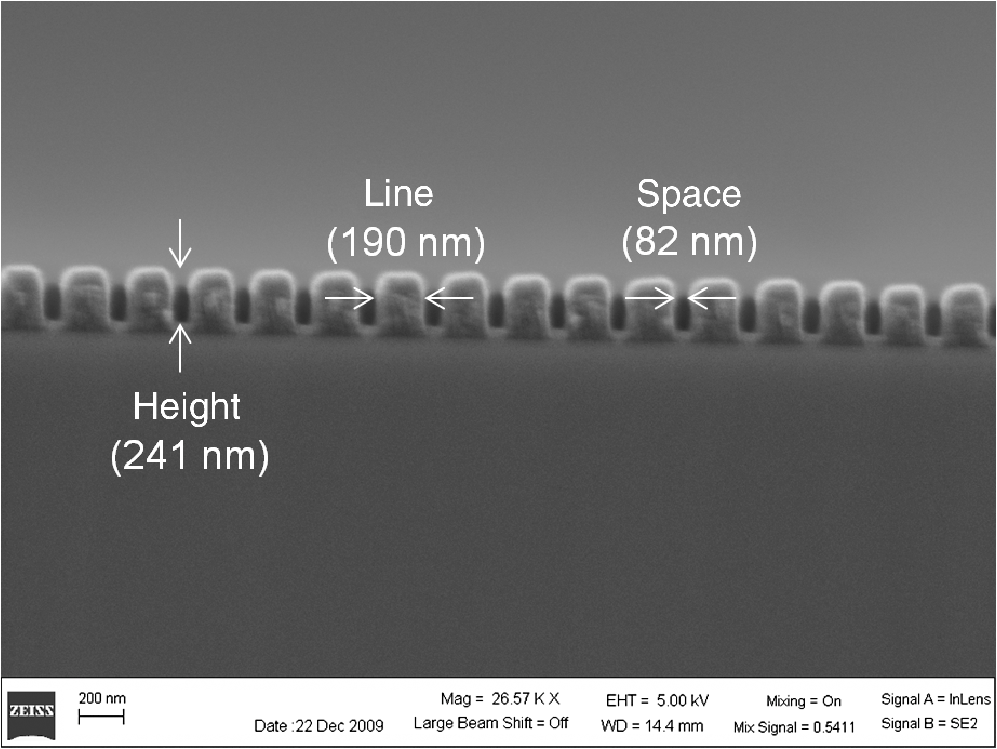
1.IntroductionStep and flash imprint lithography (S-FIL®) is one of the candidates for the fabrication of nanoscale structures such as patterned media, MEMS devices, and IC devices.1–3 S-FIL has a strong advantage over extreme ultraviolet (EUV) and other proposed optical lithography processes in terms of cost of ownership.4,5 This is because there is no need for costly optics and an expensive light source. In addition, multilevel structures can be fabricated simultaneously, which offers great cost saving in the back end of the line.6 The S-FIL process is illustrated in Fig. 1. The process can be divided into two different paths. The first is a traditional imprint process (S-FIL) and the other is a reverse-tone S-FIL process called S-FIL/R. The S-FIL/R process is superior to traditional S-FIL because of a much wider process window (high tolerance to a variety of topographic surfaces, which solves the residual layer uniformity and thickness issues) and a possibility to yield high aspect ratios.7 However, S-FIL/R requires an additional layer, a planarizing layer with high silicon content that is resistant to an plasma etch. This paper describes the development of such a planarizing material. 2.MaterialsThe material requirements for a planarizing material are outlined in Fig. 2. First, it should be resistant to an plasma etch process, and therefore a high silicon content of 12% is needed. Other properties such as low viscosity and low vapor pressure are required to achieve a good planarization of topography. We have previously reported the advantages of spin coating without a solvent to achieve planarization.8 In this case, the liquid material does not undergo a compositional change during the spin coating, thus it can be allowed to sit and planarize under surface tension forces to any desired extent after spin coating and then hardened or cured by exposure to light. Therefore, both low viscosity and low vapor pressure are important material properties. The material must incorporate structural elements that render it curable under UV exposure. There are many functional groups that crosslink under UV light. For example, epoxy, acryloyl, and vinyl functionality have all been exploited for this purpose. Considering all of these requirements led to the conclusion that branched siloxanes were strong candidates for UV curable planarizing materials. The design of a UV-curable branched siloxane was based on the previous research carried out in our laboratories. We have reported one such material, Si-14, illustrated in Fig. 3 in an earlier publication.9 Si-14 is a high molecular weight molecule (1276.48 Da) which serves to reduce the vapor pressure, and it is branched, which leads to lower viscosity. The siloxane structure contributes to the high silicon content. Methacryloyl groups were selected as the UV-curable component because of synthetic accessibility. Si-14 showed excellent planarizing properties, but the synthetic route to Si-14 required many steps and gave very poor overall yield (). The characterization of Si-14 was also tedious because of all the steps that were involved. We now report Si-12, an analog of Si-14 and a convenient synthetic path that has been developed to provide that compound in high yield. 3.Experimental Procedure3.1.Synthesis of the New Planarizing Material, Si-12The chemical structure of the UV-curable branched siloxane (epoxy-Si-12) is illustrated in Fig. 4. The number of silicon atoms has been reduced, which provides access to the greatly simplified synthetic route, and the properties of the new material are very similar to those of Si-14. Epoxide groups were selected to enable curing. Si-12 functionalized with epoxides shows a lower UV shrinkage than the corresponding methacrylate analog. The characterization of the materials was conducted by NMR (VARIAN 400 MHz, Varian Inc., Palo Alto, California), GC/MS (Agilent Technologies 6890N attached with HP-5MS capillary column, Agilent Inc., Santa Clara, California), CI-MASS (Dionex ultimate 3000, Thermo Fisher Scientific Inc., Waltham, Massachusetts), and MALDI-MASS (VARIAN Pro MALIDI 12 Tesla, Varian Inc.). 3.2.Properties of Epoxy-Si-12The weight percent of silicon in the compound is 30.0%, which far exceeds the 12% threshold normally required.10 The vapor pressure was measured by submitting a sample of Si-12 to a series of freeze–thaw cycles and then allowing the material to come to liquid–vapor equilibrium at room temperature and measuring the pressure in the vessel. The viscosity was measured by a Physica MCR 500 Rheometer (Anton Paar USA Inc., Ashland, Virginia). The UV shrinkage was calculated from the difference of film thickness on the substrates by the use of an ellipsometer (J. A. Woollam Co. Inc., Lincoln, Nebraska) before and after the UV cure. 3.3.Spin Coating of Epoxy-Si-12An initial spin coating study of epoxy-Si-12 was carried out on plain substrates. No solvent was added to the formulation. Only 0.7 wt.% of the photo acid generator (PAG) illustrated in Fig. 5 was added to the epoxy-Si-12 to initiate crosslinking under UV exposure. The spin rate of the substrates was set to 2500 rpm. A volume of 200 μl of epoxy-Si-12 was dispensed on plain substrates (), and the substrates were spun for different periods of time whereupon they were cured by exposure to UV light. The film thickness after UV exposure was measured by ellipsometry. All procedures were carried out in a yellow room (UV cutoff filtered room). 3.4.Planarizing PropertiesThe planarizing properties of epoxy-Si-12 were investigated over a patterned surface. Substrates with trench structures (width: 200 nm, depth: ) were prepared as shown in Fig. 6. Epoxy-Si-12 with PAG was spin-coated onto the test substrates at 2500 rpm for varying spin times, 15, 30, 60, 120, and 300 s, to achieve different film thicknesses. Then, each of the samples was cured by exposure to UV radiation. At two different points on the substrates, the film thickness was measured by scanning electron microscope (SEM), Zeiss Neon 40 (Carl Zeiss Microscopy, Thornwood, New York). One was the thickness over the plain substrate (). The other was the thickness over a trench structure (). The difference in height between and was assigned to . The degree of planarization (DOP) was calculated from and .11 For example, if is 0.3 μm and is 1.0 μm, DOP based on the equation below would be 70%. The experimental procedure is illustrated in Fig. 7. 3.5.S-FIL/R Demonstration Using Epoxy-Si-12An S-FIL/R demonstration was carried out using epoxy-Si-12. The process flow, the formulation used, and the target stack dimensions can be seen in Fig. 8. The process consists of several steps: (1) substrate preparation, (2) imprint test features, (3) planarization using epoxy-Si-12, (4) etch, and (5) etch. In the first step, substrates coated with an underlayer, NCI-NIL-01 (Nissan Chemical Industries, Ltd., Chiba, Japan), were prepared.12 The purpose of the underlayer or transfer layer is to improve adhesion and to provide a mask for subsequent etch process. In the second step, imprints were carried out on an Imprio 100® (Molecular Imprints Inc., Austin, Texas) S-FIL tool installed at the University of Texas at Austin. A quartz template with 80-nm lines and 180-nm spaces was fabricated by the University of Texas at Austin. The template was pretreated with a fluorinated surface treatment (tridecafluoro-1,1,2,2-tetrahydro octyldimethylchlorosilane from Gelest Inc., Morrisville, Pennsylvania) to improve the template release.13,14 In the third step, a etch was carried out on a reactive ion etcher, Oxford Plasmalab 80 plus (Oxford Instruments, Abingdon, United Kingdom) to remove the excess epoxy-Si-12 layer. The etch ratio of epoxy-Si-12 was measured to enable a timed process that led to the correct etch depth. In the last step, an etch was carried out to break through the organic layer. An SEM (Zeiss Neon 40) was used to measure the stack thicknesses and etch depths. 4.Results and Discussion4.1.Synthesis of a New Planarizing Material, Si-12A new synthetic route to Si-12 was developed and is illustrated in Fig. 9.15 The optimized route to the final product, Si-12, took only two steps. This is a tremendous improvement over the Si-14 synthesis.9 The starting materials are inexpensive and commercially available. The new synthetic route has now been shown to be easily scalable and therefore suitable for industry. Si-12 has two Si-H chemical bonds, which can used to incorporate UV curable functionality on branched siloxane. The synthetic path to epoxy-Si-12 is shown in Fig. 10. The hydrosilylation reaction16,17 was successfully carried out using a commercially available catalyst, and the pure product was recovered in high yield. The details of this synthesis will be published elsewhere. 4.2.Properties of Epoxy-Si-12Epoxy-Si-12 is a slightly yellowish liquid. It is speculated that the color of the product is due to very small amounts of residual catalyst. If the material is to be used in a metal-sensitive process, more work must be done to insure quantitative removal of the catalyst. The properties of the material are summarized in Table 1. Table 1Properties of epoxy-Si-12.
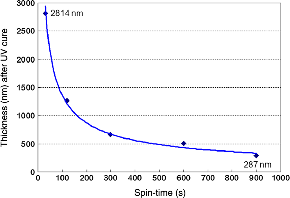
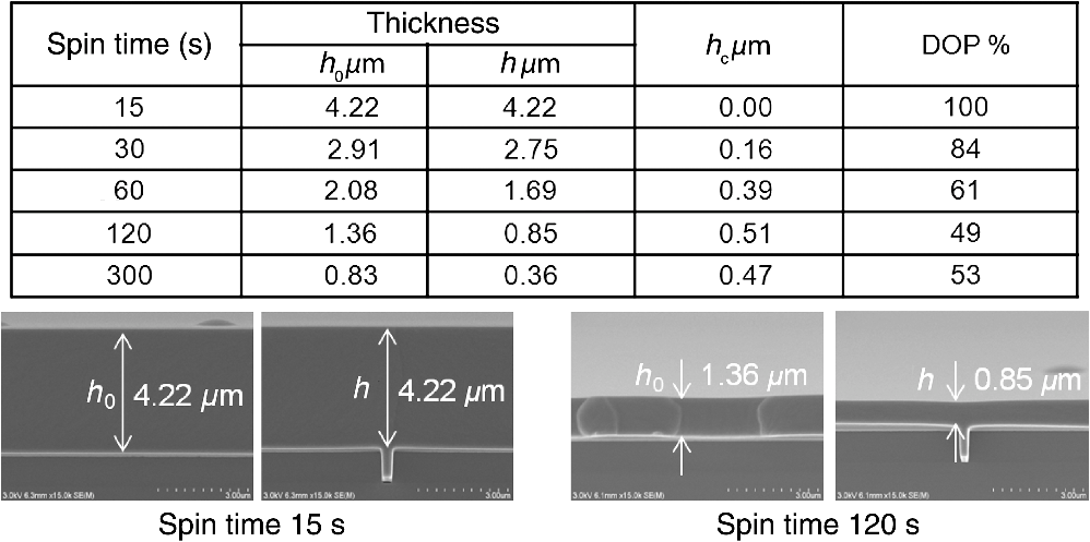
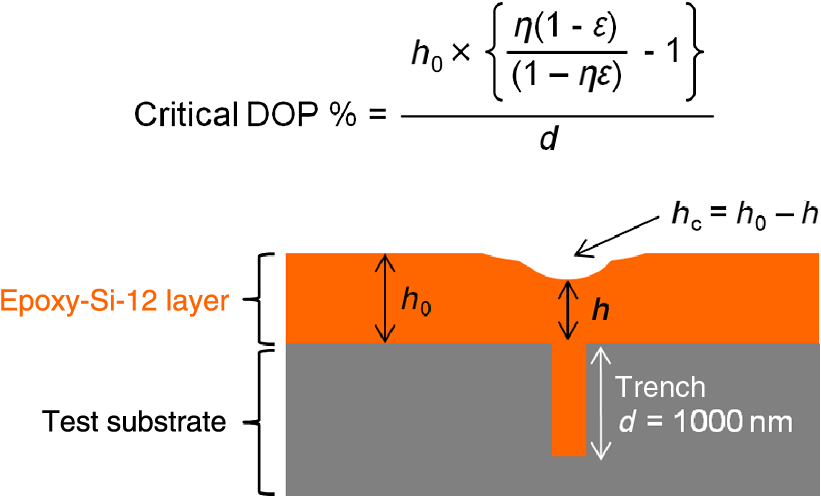
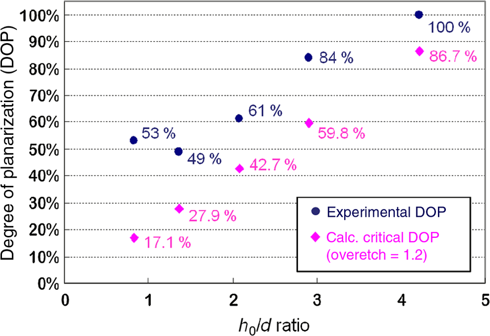
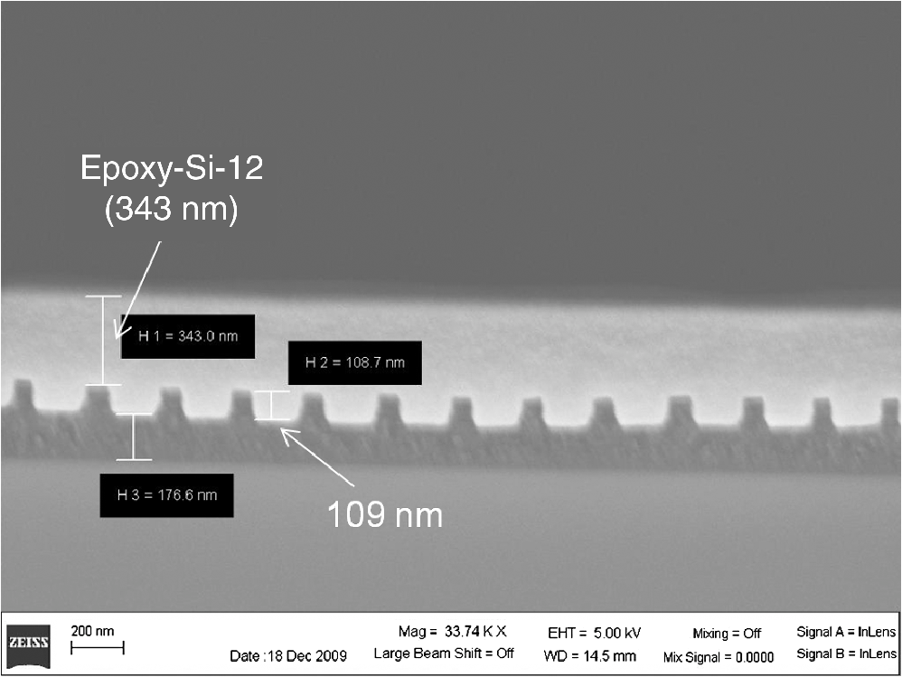
4.3.Spin-Coat Study of Epoxy-Si-12A spin curve is shown in Fig. 11. Since there is no solvent used in the process, the thickness of the film depends on the amount initially dispensed and the spin time. It should be noted that this is very different behavior which is observed when spin-coating solutions of polymers, such as photoresist. The result of this study indicated that 150 s of spin time provided a film thickness of for this substrate material and the 200-μl dispense volume. These data were useful for the subsequent planarizing studies and the S-FIL/R demonstration. 4.4.Planarizing PropertiesThe planarizing results are provided in Fig. 12. For the first experiment (15 s spin time), the value was 4.22 μm and the value was 4.22 μm, resulting in 100% DOP. But as the spin time was lengthened and decreased, the difference in film thickness () changed, which resulted in a decrease in DOP. The critical DOP values were calculated using the equation shown in Fig. 13 for comparison with the measured data.11 The value depends on the film thickness (), overetch rate (), UV shrinkage of the material (), and the trench depth (). The critical DOP is the minimum requirement for a successful etch process. Figure 14 shows the correlation between ratios and DOP values. All experimental DOP values met the critical DOP requirement. The results indicate that epoxy-Si-12 has the potential to be an excellent planarizing layer for subsequent processes. In future work, simulations of the planarizing process could be useful for the discussion of the planarizing properties of epoxy-Si-12, especially the DOP value at 300-s spin time where the results did not follow the general trend. Further planarizing studies using different test substrates and patterns such as multiple trenches, or via structures, are required to fully understand the planarizing properties of epoxy-Si-12. 4.5.S-FIL/R Demonstration Using Epoxy-Si-12 ResistFollowing are the results of each step in the S-FIL/R process:
5.ConclusionThis paper describes a UV-curable branched siloxane, epoxy-Si-12, that is useful for a planarizing material of the sort required for S-FIL/R. Epoxy-Si-12 was synthesized via a convenient new route in high yield. The properties of epoxy-Si-12 indicated low viscosity (29 cP at 25°C), low vapor pressure (0.65 Torr at 25°C), and high Si content (30.0%), which meet all the requirements for a planarizing material for S-FIL/R. Epoxy-Si-12 showed excellent planarizing properties, and it easily met the critical DOP in the topography structure studied. S-FIL/R using epoxy-Si-12 was successfully demonstrated, and the desired reverse-tone pattern was obtained successfully after the etch process. Other UV-curable Si-12 derivatives, such as methacryloyl-Si-12 etc., are being studied currently. AcknowledgmentsThe authors want to thank Nissan Chemical Industries Inc., Japan, for generous funding. The authors want to thank Dr. Kazuhiko Maeda and Central Glass Co. Ltd., Japan, for support of Mr. Tsuyoshi Ogawa and for valuable advice on the chemistry of branched siloxanes. The authors would also like to thank Dr. Marylene Palard, Mr. Gabriel Glenn, and Mr. Ricardo Garcia of the University of Texas at Austin for technical advice and support of the S-FIL/R demonstration. ReferencesM. Colburnet al.,
“Step and flash imprint lithography: a new approach to high resolution patterning,”
Proc. SPIE, 3676 379
–389
(1999). http://dx.doi.org/10.1117/12.351155 PSISDG 0277-786X Google Scholar
C. G. Willson,
“A decade of step and flash imprint lithography,”
J. Photopolym. Sci. Technol., 22
(2), 147
–153
(2009). http://dx.doi.org/10.2494/photopolymer.22.147 JSTEEW 0914-9244 Google Scholar
T. Higashikiet al.,
“Nanoimprint lithography and future patterning for semiconductor devices,”
J. Micro/Nanolithogr. MEMS MOEMS, 10
(4), 043008
(2011). http://dx.doi.org/10.1117/1.3658024 JMMMHG 1932-5150 Google Scholar
L. Litt,
“Sematech,”
in 7th Int. Conf. on Nanoimprint and Nanoprint Technology (NNT’08),
(2008). Google Scholar
S. V. Postnikov,
“Infineon Technologies,”
in Semicon Europa,
(2007). Google Scholar
F. Palmieriet al.,
“Multi-level step and flash imprint lithography for direct patterning of dielectrics,”
Proc. SPIE, 6151 61510J
(2006). http://dx.doi.org/10.1117/12.655604 PSISDG 0277-786X Google Scholar
S. V. Sreenivasanet al.,
“Using reverse-tone bilayer etch in ultraviolet nanoimprint lithography,”
Micromagazine,
(2001). Google Scholar
M. W. Linet al.,
“Planarization for reverse-tone step and flash imprint lithography,”
Proc. SPIE, 6151 61512G
(2006). http://dx.doi.org/10.1117/12.655626 PSISDG 0277-786X Google Scholar
J. Haoet al.,
“Photocurable silicon-based materials for imprint lithography,”
Proc. SPIE, 6517 651729
(2007). http://dx.doi.org/10.1117/12.712261 PSISDG 0277-786X Google Scholar
M. Colburnet al.,
“Step and flash imprint lithography for sub-100 nm patterning,”
Proc. SPIE, 3997 453
–457
(2000). http://dx.doi.org/10.1117/12.390082 PSISDG 0277-786X Google Scholar
M. W. Linet al.,
“Simulation and design of planarizing materials for reverse-tone step and flash imprint lithography,”
J. Micro/Nanolithogr. MEMS MOEMS, 7
(2), 023008
(2008). http://dx.doi.org/10.1117/1.2896047 JMMMHG 1932-5150 Google Scholar
S. Takeiet al.,
“Silicon-containing spin-on underlayer material for step and flash nanoimprint lithography,”
Jpn. J. Appl. Phys., 49
(7R), 075201
(2010). http://dx.doi.org/10.1143/JJAP.49.075201 JJAPA5 0021-4922 Google Scholar
T. Baileyet al.,
“Step and flash imprint lithography: template surface treatment and defect analysis,”
J. Vac. Sci. Technol. B, 18
(6), 3572
–3577
(2000). http://dx.doi.org/10.1116/1.1324618 JVTBD9 0734-211X Google Scholar
T. Ogawaet al.,
“Reactive fluorinated surfactant for step and flash imprint lithography,”
J. Micro/Nanolithogr. MEMS MOEMS, 12
(3), 031114
(2013). http://dx.doi.org/10.1117/1.JMM.12.3.031114 JMMMHG 1932-5150 Google Scholar
K. Yoshinoet al.,
“A convenient synthesis of , -difunctionalized linear dimethylsiloxanes with definite chain lengths,”
Chem. Lett., 19
(11), 2133
–2136
(1990). http://dx.doi.org/10.1246/cl.1990.2133 CMLTAG 0366-7022 Google Scholar
C. Zhanget al.,
“Hydrosilylation of allyl alcohol with : octa(3-hydroxypropyldimethylsiloxy)octasilsesquioxane and its octamethacrylate derivative as potential precursors to hybrid nanocomposites,”
J. Am. Chem. Soc., 122
(29), 6979
–6988
(2000). http://dx.doi.org/10.1021/ja000318r JACSAT 0002-7863 Google Scholar
T. Ogawaet al.,
“Ultraviolet curable branched siloxanes as low-k dielectrics for imprint Lithography,”
J. Vac. Sci. Technol. B, 31
(1), 011601
(2013). http://dx.doi.org/10.1116/1.4770051 JVTBD9 0734-211X Google Scholar
|