|
|
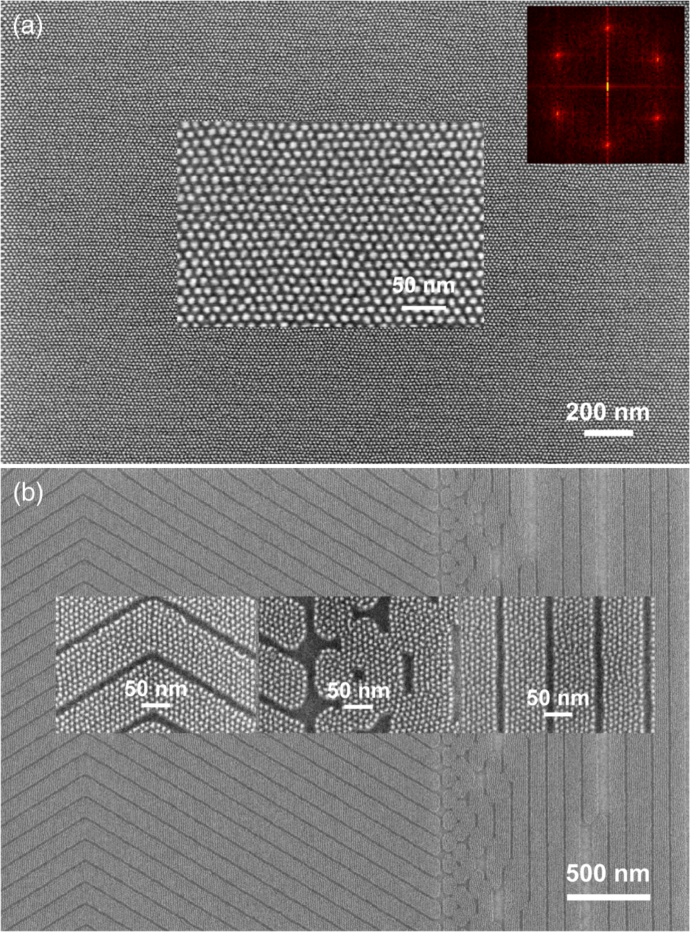
1.IntroductionThe ever-increasing demand for higher capacity information storage is forcing the magnetic storage industry to develop alternative technologies to the currently adopted perpendicular magnetic recording.1 One of the leading technological candidates for extending current perpendicular magnetic recording beyond () is the bit-patterned media (BPM) technology, in which magnetic nanoarrays are fabricated and each “island” in the array forms a separate recording bit at a sub-25-nm length scale.2,3 BPM application presents extreme challenges to today’s lithography capability because of the small feature size and the tight spacing tolerance requirements.4 A promising approach is the directed copolymer assembly, which combines top-down advanced lithography with bottom-up self-assembling block copolymer (BCP) materials. Self-assembling BCP materials can readily form highly ordered periodic patterns with a variety of morphologies, such as spheres, cylinders, and lamellae at a length scale of 5 to 50 nm.5–10 Directed self-assembly (DSA) of BCP has been successfully proven through experiments to be a good solution for the high density BPM application. So far, two major approaches have been proposed. One approach is to form hexagonal BPM by using either cylinder-forming (Refs. 1011.12.–13) or sphere-forming ,14–17 and the other approach is to form rectangular BPM by using lamellae-forming .18,19 However, most of these fabrication works previously reported focused on the data zone demonstration, including an all-dots template fabrication, imprint lithography, and magnetic dots formation. Because of the nature of the information stored in servo zones, the geometry and shape of the servo patterns are different from those in the data zones. In other words, the servo layouts require more complex patterns than the simple arrays naturally achieved by the DSA process. Therefore, integrating a servo design with the DSA process is still challenging. In order to solve this issue, two research groups have been working on their own approaches. Researchers at Hitachi Global Storage Technologies (HGST) have demonstrated a servo design that uses a lamellae-forming BCP on chemical patterns to create a chevron shaped servo pattern.20 However, they have not transferred the servo patterns onto a magnetic layer. The data zone is still a lamellar line pattern and it is not cut into rectangular bits. Another group of researchers from Toshiba demonstrated a BPM disk with a ridge-and-groove servo pattern by directly using sphere-forming BCP as an etching mask.21–23 A drawback of using the groove guided DSA process in both the data and the servo regions at the same time is the real-estate loss and the challenge in dot-position control guided by graphoepitaxy in the data area. Using DSA with a two-dimensional (2-D) dot-array prepattern in the data area overcomes this problem. Further, neither one of the approaches mentioned above are completed at the template level. There is no report so far on how to fabricate a BPM template with fully integrated servo patterns using the DSA process. In this work, we will focus on fabricating a servo-integrated BPM template based on sphere-forming BCP patterns. A novel strategy to integrate a complex servo design with a simple DSA process has been proposed. This proposed method is based on an imprint guided two-step DSA process, combined with conventional optical lithography to define two separate zones. Both the data zone and servo zone consist of hexagonal self-assembled dot-array patterns: a regular pattern in the data zone and a complex pattern in the servo zone. We have successfully applied this method to fabricate a servo-integrated BPM quartz template at a density of . Using the fabricated quartz template, CoCrPt magnetic media has been successfully patterned by nanoimprint lithography (NIL) and a subsequent ion-beam etching (IBE) process on standard 2.5 in. disks. Further, using patterned-in servo wedges on patterned CoCrPt media, we are able to close the servo control loop for track-following on a spin-stand tester. The close-servo-loop success directly validates the functionality of our servo-integrated BPM template fabricated using our imprint guided two-step DSA method. 2.Experimental ProcedureThe 150-mm diameter fused silica wafers were purchased from Shin-Etsu Chemical Co. (Tokyo, Japan), and used as substrates for BPM nanoimprint template fabrication. All BCP materials were purchased from Polymer Source Inc. (Quebec, Canada) Sphere-forming BCP materials with different molecular weights were used in our DSA experiments. The homopolymer polystyrene (PS) has a of ( is the number-average molar mass) with a polydispersity of 1.09. As previously reported in our earlier study, in order to get BCP pattern with a special period number, two BCPs with different molecular weights are needed to mix at a certain weight ratio. For example, to get a BCP pattern with , which corresponds to in pattern density, the () powder was mixed with () powder and homopolymer PS at a ratio of 4:3:1 (wt./wt.). The mono-hydroxyl-terminated polystyrene (PS-OH) with a of was used as the brush layer for modifying the substrate for better DSA. The imprint resist was purchased from Molecular Imprints Inc. (Austin) All other chemicals were purchased from Sigma-Aldrich (St. Louis). A pillar-tone seed imprint template was fabricated using a rotary EBW system operating at 100 keV and reactive ion etching (RIE) (Oxford Plasmalab, Santa Barbara system 100). The nanoimprint process was performed with two imprint tools purchased from Molecular Imprints Inc. One is the Perfecta TR1100 (Austin) for 150-mm diameter fused silica template fabrication and the other is the Imprio 1100 for 2.5 in. imprint on disks. The imprint resist is FT247 purchased from Molecular Imprints. Before imprint, a 1- to 2-nm thick Transpin adhesion layer was deposited onto a quartz substrate by spin coating. A monolayer film of sphere-forming was spin-coated on the substrate and then annealed in a vacuum oven at 170°C for approximately 12 h to reach the BCP equilibrium state. After the DSA process, the thin film was first treated by RIE for 7 s and then the PS blocks were removed by RIE for 30 to 60 s. Optical lithography was done using Karl Suss MA6 Mask Aligner (Sunnyvale)with I-line (365 nm) photoresists. The BCP thin film thickness was determined using the NanoSpec 6100 (Milpitas, California) system from Nanometrics. Scanning electron microscopy (SEM) characterization was conducted using the Raith 150 (New York) system operating at 10 keV. A 3-nm thick Cr layer was sputtered (ATC 2200 from AJA International, Inc., North Scituate) on fused silica wafers to minimize the charging effect. Magnetic materials were etched using IBE. The magnetic loop was measured by an in-house magnetometer. Atomic force microscopy (AFM) measurements were performed in the tapping mode with a NanoScope D3100 (Plainview) system from Veeco Digital Instruments. 2-D Fourier transforms were obtained from SEM images using FTL-SE software. Size sigma and position accuracy analyses were performed based on high-quality SEM images and commercial software purchased from Simagis (Houston). 3.Results and DiscussionAs mentioned above, one of the most challenging aspects of using the DSA for BPM template fabrication is the servo pattern integration. A BPM disk consists of two different pattern regions. One is called the data zone, which is used for storing data. The other is called the servo zone, which is used to describe the data in the data zone. The servo zone is a vital area that contains information required for head positioning, timing, and track-following for the adjacent data zone. Due to the different functionalities of these two regions, they require patterns with different geometries and shapes. For instance, the data zone requires a globally addressable all-dots array, whereas the servo zone requires a locally aligned segment dots array. In template fabrication, in order to use the DSA to create the intricate servo design, both the data zone and servo zone need to go through the DSA process. Because of the different pattern shapes in these two zones, the guiding prepatterns do not have to be the same. As reported in our previous studies,15,16 a 2-D dot-array prepattern, either a chemical or a low-topographic contrast pattern, can be used for the DSA in the data zone, whereas a one-dimensional (1-D) groove prepattern for the servo shape is more suitable for the DSA in the servo zone since the groove guide can provide an arbitrary shape. Furthermore, through our imprint guided two-step DSA method, these two types of prepatterns can be simultaneously created via a single imprint step by imprint lithography. Figure 1 schematically illustrates the servo pattern integration scheme of our proposed imprint guided two-step DSA process. A thin imprint resist layer containing two pattern regions is created using imprint lithography and then the imprinted resist pattern will be used as a copolymer guiding prepattern for DSA. The data zone has a 2-D hole-tone dot-array pattern at a low density of , whereas the servo zone has many 1-D grooves in the shape of servo patterns. With this method, optical lithography is used to define these two separate zones: data zone and servo zone, so the two DSA processes and subsequent pattern transfer process can be separately optimized in order to achieve the best DSA and pattern transfer results for each zone. For example, while processing the data zone, the servo zone is protected by an optical resist. The imprint resist thickness in the data zone can be trimmed down even more to 2 to 3 nm in order to minimize topographical effects for the best pattern transfer results in the data zone. However, in the servo zone, a certain groove height in the resist prepattern, ranging from 20 to 30 nm, is necessary in order to guide the DSA of the BCP along the groove sidewall. Since the sphere-forming BCP film with a monolayer thickness was used for the data zone and servo zone, the concentration of the BCP solution needs be separately optimized. It should be noted here that two DSA steps are not always necessary in our proposed approach. It can be done in one-single DSA step if the cylinder-forming BCP film, such as BCP film, is used in both the data area and the servo area, as previously reported.24 However, it has been proven that has a higher Flory–Huggins interaction parameter value of 0.26 than that of other BCP materials, such as of 0.06. With the commercially available cylinder-forming BCP material, the highest BCP density with the lowest molecular weight is about . The high value BCP material allows us to conduct the process development for higher densities up to 4 to .14,16 Once the first DSA process in the data zone is completed, the BCP patterns are subsequently transferred into the underlying quartz substrate through a Cr hard mask layer to form pillar-tone quartz dots in the data zone. A similar processing flow can be applied to the servo zone. Unlike the data zone, the servo zone uses a 1-D groove prepattern as guiding patterns for the second DSA process. Finally, a servo-integrated BPM template is fabricated after two DSA steps based on this integration scheme. Fig. 1Schematical illustration of the imprint guided two-step directed self-assembly (DSA) process for servo pattern integration. (a) A imprint resist layer containing two pattern regions is created using nanoimprint lithography. The data zone is a two-dimensional (2-D) hole-tone dot-array pattern at , whereas the servo zone consists of many one-dimensional grooves in the shape of servo patterns. (b) Optical lithography is used to open the data zone and protect the servo zone. Trimming imprint resist thickness down to 2 to 3 nm. (c) First DSA of sphere-forming in the data zone. The density multiplication factor is 2 in this example (). (d) Pattern transfer from BCP patterns to Cr hard mask layer. (e) Pattern transfer from Cr layer into quartz substrate to form pillars in the data zone. (f) Optical lithography is used to open the servo zone and protect the data zone. Trimming imprint resist thickness down to a range of 20 to 30 nm. (g) Second DSA of spherical-forming () in the servo zone. (h) Pattern transfer from BCP patterns to Cr hard mask layer. (i) Pattern transfer from Cr into quartz substrate to form pillars in the servo zone. (j) Finally, template is cleaned using piranha solution. 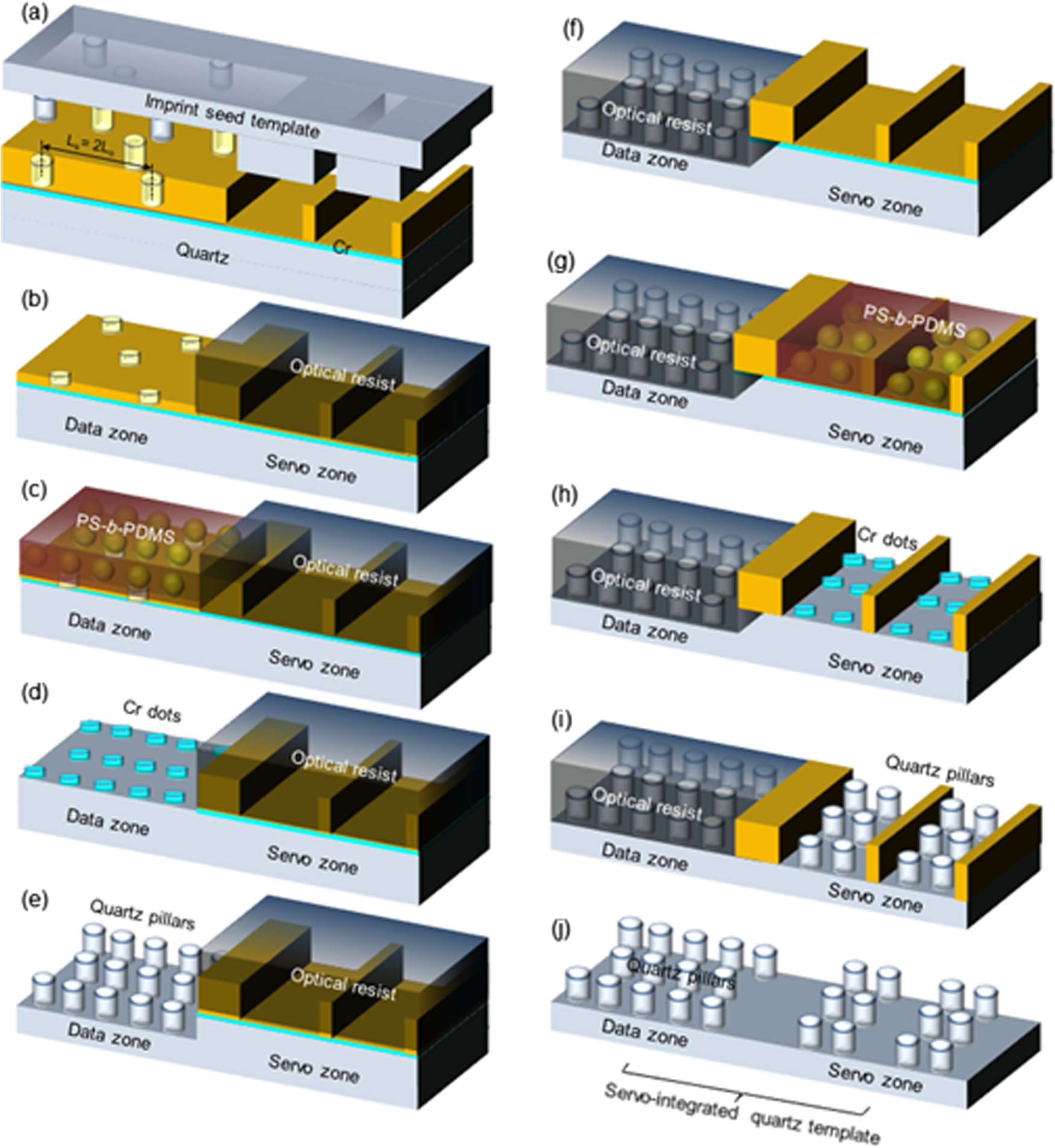 The servo integration scheme proposed here is a simpler method that requires one standard NIL process followed by two DSA steps. The NIL process can be either the UV imprint or the thermal imprint process. In the process development stage, the NIL can save tremendous e-beam writing time for DSA template creation. Also, our NIL tool has a built-in resist coating function and no development step is needed, while the e-beam requires separate coating and development steps. Therefore, the simpler the prepattern process is, the better the DSA is for BPM manufacture. A servo-integrated template at a density of has been fabricated using our proposed integration scheme, as shown in Fig. 2. These SEM images show the fabrication steps starting from the imprint prepatterns to DSA, including the final pillar-tone quartz etching through the data zone and servo zone based on our imprint guided two-step DSA process. The data zone is a 2-D hole-tone dot-array pattern (hcp) at a low density of [see Fig. 2(a)], whereas the servo zone consists of many different shapes of groove patterns with a complex servo layout [see Figs. 2(d), 2(g), and 2(j)]. After an imprint process, the resist thickness in the data zone needs to be further reduced to a thickness range of 2 to 3 nm using RIE. The trimmed resist pattern is then modified with a PS-OH brush for a better BCP film wettability. As shown in Figs. 2(e), 2(h), and 2(k), all PDMS spheres in the servo zone have integral row numbers from 3 to 6, and they are well aligned to the groove sidewalls. Some extra amounts of the BCP films sitting outside the grooves can be easily removed by RIE after a DSA process. Fig. 2Scanning electron microscopy (SEM) images show the three fabrication steps: imprint prepattern, DSA, and quartz etch in the data zone (a–c) and servo zone (d–l). (a) imprint prepattern for DSA in the data zone. (b) PDMS spheres after DSA. (c) quartz dots after pattern transfer. (d), (g), and (j) are three imprint servo groove prepatterns. They correspond to position error signal (PES), gray code, and phase lock loop (PLL), respectively. (e), (h), and (k) are PDMS spheres after DSA in the servo zone. (f), (i), and (l) are the corresponding quartz dots after etch in the servo zone. 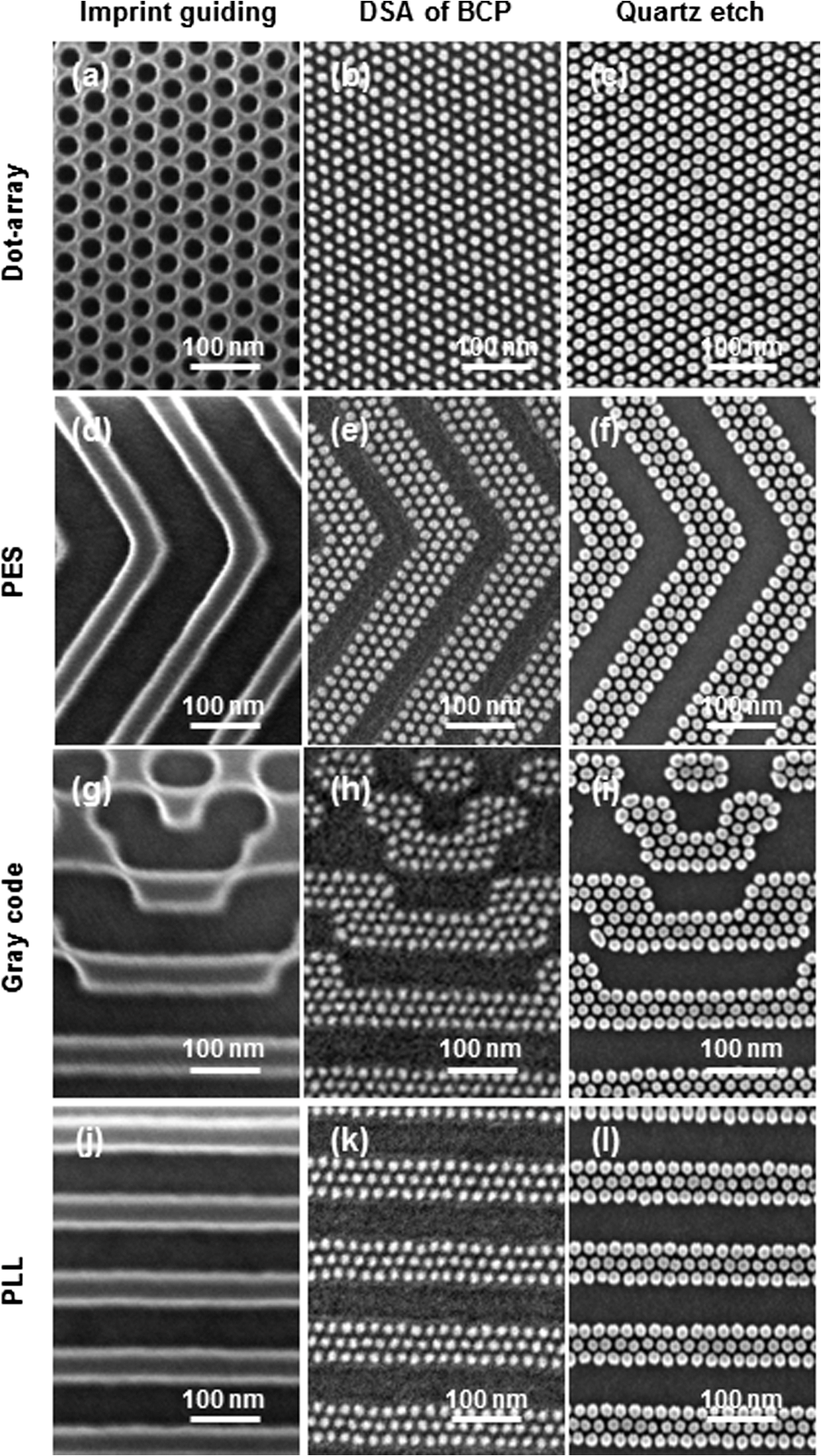 Figure 3(a) shows an SEM image of a fabricated template with a 2.4-mm-wide band of circular tracks. The full track consists of two regions: data zone and servo zone (shown in the inset). The 2.4-mm-wide band was divided into three subzones using a zoning strategy to accommodate the pitch variation restriction in the BCP patterns. Each subzone has a band width of . The surface prepattern pitch from each subzone is reset to 22.3 nm to exactly match the BCP natural pitch exactly. Therefore, the BCP commensurability (either stretching or compressing the polymer chains) is controlled within their dimensional restriction of range in each subzone. Under this restriction, the BCP can still follow the underlying surface prepattern to form a defect-free pattern with a good long-range ordering. Figure 3(b) shows a cross-sectional SEM image. The etched quartz pillar height is approximately 25 nm. Four zoom-in SEM images from different locations in the data zone are shown in Figs. 3(c)–3(f). Figure 4(a) illustrates a large-scale top-down SEM image of a template that shows an overview of the servo zone area. The three-dimensional AFM and titled SEM images shown in Figs. 4(b)–4(e) show the several fabricated typical BPM servo patterns. They correspond to gray code, position error signal (PES), phase lock loop, and address mark, respectively. It is clearly visible from all SEM and AFM images here that a high-quality quartz template has been achieved using our fabrication method and process. Our AFM measurements (not shown here) indicated that the template has good pattern uniformity with a top height variation of 2 to 3 nm over the entire zone area. Image analysis for evaluating both the size sigma and the position accuracy is used in all fabrication steps to monitor each process. The dot placement accuracy (pitch variation) of () and the size sigma (diameter variation) of () have been achieved in our final template. The defect density, such as missing dots, connected dots, or too small dots, calculated in the final template is on the order of about over the entire data and servo zone areas. The high quality of the fabricated template is a direct result of the benefits of utilizing the DSA process as opposed to utilizing a conventional e-beam lithography process. Fig. 3(a) Large-scale top-down SEM image of a fabricated template with a 2.4-mm-wide band of circular track. The full track consists of two regions: data zone and servo zone (shown in the inset). (b) Cross-sectional SEM image of data zone. The etched quartz pillar height is approximately 25 nm. (c) to (f) are zoom-in SEM images of data zone taken from the north, west, east, and south four locations from the data zone, respectively. 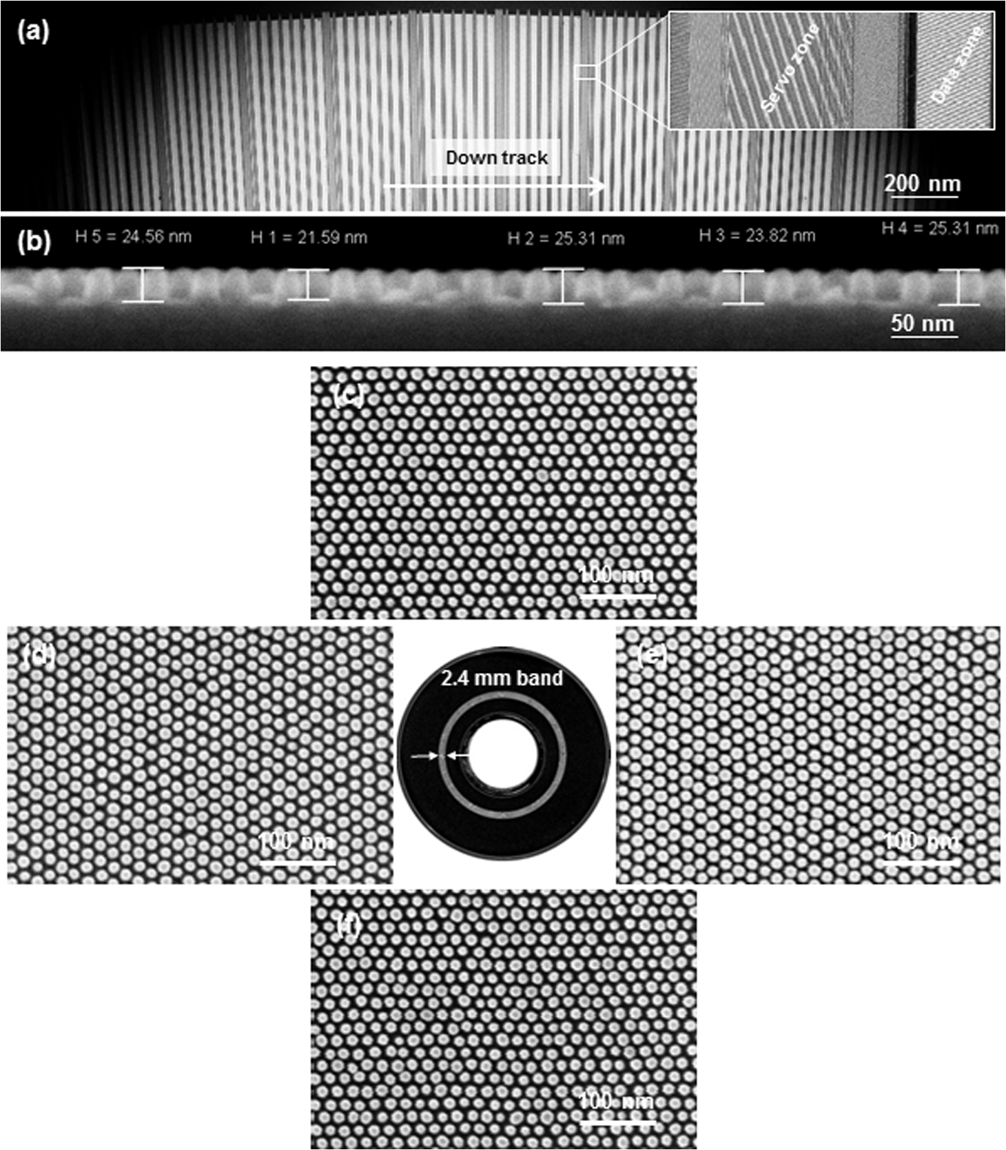 Fig. 4(a) Large-scale top-down SEM image of a fabricated servo-integrated BPM template, showing both the servo zone and adjacent data zone. The three-dimensional AFM images show three different servo patterns. (b) to (e) are titled zoom-in SEM images showing various servo patterns, corresponding to the servo patterns of gray code, PES, PLL, and address mark, respectively.  To further explore the efficiency of using our fabricated template for media fabrication, we have conducted imprint lithography process development on standard 2.5 in. size disks. The progress and challenges of BPM imprint lithography on disks have been discussed in our previous studies.25,26 After imprint, a reverse tone process is applied to convert the initial imprint resist hole-tone pattern into a silicon oxide pillar-tone pattern using HSQ spin coating first and then etching back with CF4 RIE. Then, in preparation for next magnetic material etch, the silicon oxide pillar-tone pattern is used as an etching mask to etch into a thin carbon hard mask. Figure 5(a) shows an SEM image of the 8-nm thick CoCrPt media formed using IBE. The magnetic loop with a high coercivity of approximately 7 kOe is shown in Fig. 5(b). The final success of forming a patterned magnetic media on a disk verifies the functionality of the template fabricated using our imprint guided two-step DSA process. Fig. 5(a) Top-down SEM image of patterned CoCrPt media from the data zone. (b) Corresponded magnetic hysteresis loop. 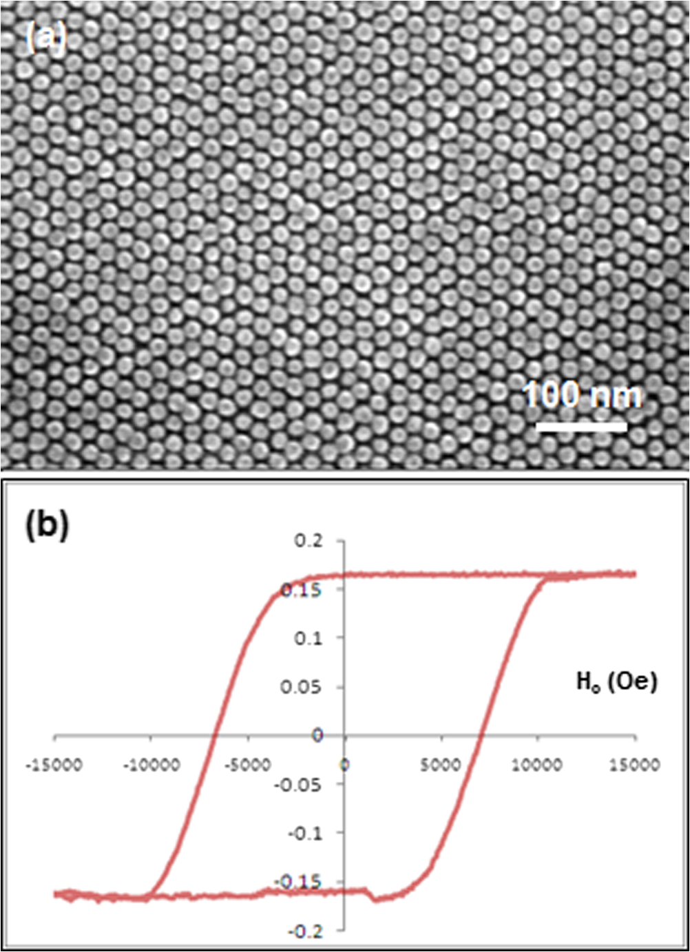 The fabricated media was further tested on a spin-stand equipped with a high-bandwidth actuator under a closed-loop servo control. The test was conducted at the spindle speed of 6000 rpm, with an estimated head-to-media clearance of 1.5 nm. Figure 6(a) shows the PES demodulated by a hardware channel on the basis of the read-back signal from the patterned-in servo wedges. PES was plotted as a function of angular location for more than 700 revolutions (green) in the unit of track pitch (TP), which is 38.6 nm. Repeatable run-out (RRO), represented by the mean of PES (red) from multiple reads, is also shown in Fig. 6(a). The standard deviation (sigma) of RRO over the full revolution is calculated to be about 4% of the track pitch. The data demonstrates that the integrated servo patterns fabricated using the imprint guided DSA approach can provide precise positional information, and that the recording head can be accurately positioned at the desired track center to perform recording operations. The head read-back signal for one servo wedge across 20 tracks is plotted in a 2-D color map in Fig. 6(b). Compared with the fabricated servo patterns in a template, shown in the SEM of Fig. 6(c), it clearly indicates that all the servo pattern features were faithfully transferred from the template to the magnetic media by the NIL and subsequent media patterning processes, and were successfully read-back by a recording head for the closed-loop servo control mentioned above. Fig. 6(a) A commercial channel was used to demodulate the servo position information for more than 700 revolutions (green). The RRO is represented by the mean of PES (red) from multiple reads. (b) An image of a single servo wedge, assembled out of read-back waveforms from a head flying over the disk. (c) SEM image of the corresponded servo zone from a fabricated quartz template. 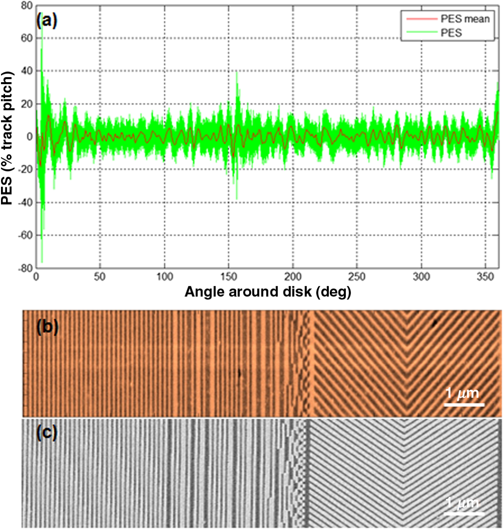 Through demonstrating our proposed integration scheme with an even higher density, we have extended our process to (). Figures 7(a) and 7(b) show SEM images of a sphere-forming BCP pattern at () in the data zone and servo zone, respectively. As is visible in the illustration, the BCP spheres align very well with the underlying prepatterns in both the data zone and servo zone. The pattern transfer process under this high density, however, is currently under development. More research will lead to further innovation. 4.ConclusionsA strategy to integrate the servo pattern design with the DSA process has been proposed for servo-integration in BPM template fabrication. This proposed method is based on an imprint guided two-step DSA process, combined with conventional optical lithography to define separate zones. This method was successfully used to fabricate a servo-integrated template at a density of . Using the fabricated quartz template, CoCrPt BPM media has been successfully patterned by the NIL and subsequent IBE process on a 2.5 in. disk. Furthermore, through using patterned-in servo wedges on a CoCrPt media, we are able to close the servo control loop for track-following on a spin-stand tester. The standard deviation of RRO over the full revolution is calculated to be about 4% of the 38.6 nm track pitch. This track-following success on a spin-stand tester validates the functionality of our servo-integrated template fabricated using our proposed imprint guided two-step DSA process. AcknowledgmentsThe authors would like to thank many colleagues at Seagate Media Research for their experimental assistance and helpful discussions, including Michael Feldbaum, Zhaoning Yu, Nobuo Kurataka, and Gene Gauzner. ReferencesS. N. Piramanayagam,
“Perpendicular recording media for hard disk drives,”
J. Appl. Phys., 102
(1), 011301
(2007). http://dx.doi.org/10.1063/1.2750414 JAPIAU 0021-8979 Google Scholar
C. R. Ross,
“Patterned magnetic recording media,”
Ann. Rev. Mater. Res., 8
(31), 203
–235
(2001). http://dx.doi.org/10.1146/annurev.matsci.31.1.203 ARMRCU 1531-7331 Google Scholar
E. A. Dobiszet al.,
“Patterned media: nanofabrication challenges of future disk drives,”
Proc. IEEE, 96
(11), 1836
–1846
(2008). http://dx.doi.org/10.1109/JPROC.2008.2007600 IEEPAD 0018-9219 Google Scholar
H. J. Richteret al.,
“Recording potential of bit-patterned media,”
Appl. Phys. Lett., 88
(22), 222512
–222514
(2006). http://dx.doi.org/10.1063/1.2209179 APPLAB 0003-6951 Google Scholar
X.-M. Yanget al.,
“Guided self-assembly of symmetric diblock copolymer films on chemically nanopatterned substrates,”
Macromolecules, 33
(26), 9575
–9582
(2000). http://dx.doi.org/10.1021/ma001326v MAMOBX 0024-9297 Google Scholar
S. O. Kimet al.,
“Epitaxial self-assembly of block copolymers on lithographically defined nanopatterned substrates,”
Nature, 424
(6947), 411
–414
(2003). http://dx.doi.org/10.1038/nature01775 NATUAS 0028-0836 Google Scholar
M. P. Stoykovicet al.,
“Directed assembly of block copolymer blends into nonregular device-oriented structures,”
Science, 308
(5727), 1442
–1446
(2005). http://dx.doi.org/10.1126/science.1111041 SCIEAS 0036-8075 Google Scholar
I. Bitaet al.,
“Graphoepitaxy of self-assembled block copolymers on two-dimensional periodic patterned templates,”
Science, 321
(5891), 939
–943
(2008). http://dx.doi.org/10.1126/science.1159352 SCIEAS 0036-8075 Google Scholar
J. Y. Chenget al.,
“Dense self-assembly on sparse chemical patterns: rectifying and multiplying lithographic patterns using block copolymers,”
Adv. Mater., 20
(16), 3155
–3158
(2008). http://dx.doi.org/10.1002/adma.v20:16 ADVMEW 0935-9648 Google Scholar
R. Ruizet al.,
“Density multiplication and improved lithography by directed block copolymer assembly,”
Science, 321
(5891), 936
–939
(2008). http://dx.doi.org/10.1126/science.1157626 SCIEAS 0036-8075 Google Scholar
X.-M. Yanget al.,
“Directed block copolymer assembly versus electron beam lithography for bit patterned media with areal density of 2 and beyond,”
ACS Nano, 3
(7), 1844
–1858
(2009). http://dx.doi.org/10.1021/nn900073r 1936-0851 Google Scholar
T. R. Albrechtet al.,
“Bit patterned media at 2 and beyond,”
IEEE Trans. Magn., 49
(2), 773
–778
(2013). http://dx.doi.org/10.1109/TMAG.2012.2227303 IEMGAQ 0018-9464 Google Scholar
L. Wanet al.,
“Directed self-assembly of cylinder-forming block copolymer: prepatterning effect on pattern quality and density multiplication factor,”
Langmuir, 25
(21), 12408
–12413
(2009). http://dx.doi.org/10.1021/la901648y LANGD5 0743-7463 Google Scholar
S. Xiaet al.,
“A general approach to addressable 4 Td/in. patterned media,”
Adv. Mater., 21
(24), 2516
–2519
(2009). http://dx.doi.org/10.1002/adma.v21:24 ADVMEW 0935-9648 Google Scholar
S. Xiaoet al.,
“Directed self-assembly for high-density bit-patterned media fabrication using spherical block copolymers,”
J. Micro/Nanolith. MEMS MOEMS, 12
(3), 031110
(2013). http://dx.doi.org/10.1117/1.JMM.12.3.031110 JMMMGF 1932-5134 Google Scholar
X.-M. Yanget al.,
“Directed self-assembly of block copolymer for bit patterned media with areal density of 1.5 Teradot/inch2 and beyond,”
J. Nanomater., 2013 17
(2013). JNOABP 1687-4129 Google Scholar
S. Xiaoet al.,
“A facile route to regular and nonregular dot arrays by integrating nanoimprint lithography with sphere-forming block copolymer directed self-assembly,”
J. Polym. Sci. Part B, 52
(5), 361
–367
(2014). http://dx.doi.org/10.1002/polb.v52.5 JPLPAY 0887-6266 Google Scholar
R. Ruizet al.,
“Rectangular patterns using block copolymer directed assembly for high bit aspect ratio patterned media,”
ACS Nano, 5
(1), 79
–84
(2011). http://dx.doi.org/10.1021/nn101561p 1936-0851 Google Scholar
L. Wanet al.,
“Fabrication of templates with rectangular bits on circular tracks by combining block copolymer directed self-assembly and nanoimprint lithography,”
J. Micro/Nanolith. MEMS MOEMS, 11
(3), 031405
(2012). http://dx.doi.org/10.1117/1.JMM.11.3.031405 JMMMGF 1932-5134 Google Scholar
G. L. Liuet al.,
“Fabrication of chevron patterns for patterned media with block copolymer directed assembly,”
J. Vac. Sci. Technol. B, 29 06F204
(2011). JVTBD9 0734-211X Google Scholar
N. Kiharaet al.,
“Fabrication of 2 bit patterned media with servo pattern using directed self-assembly,”
J. Vac. Sci. Technol. B, 30 06FH02
(2012). http://dx.doi.org/10.1116/1.4763356 JVTBD9 0734-211X Google Scholar
R. Yamamotoet al.,
“Nanoimprint mold for 2 directed self-assembly bit patterned media with phase servo pattern,”
Jpn. J. Appl. Phys., 51 046503
(2012). JJAPA5 0021-4922 Google Scholar
Y. Kamataet al.,
“Fabrication of ridge-and-groove servo pattern consisting of self-assembled dots for 2 bit patterned media,”
IEEE Trans. Magn., 47 51
–54
(2011). http://dx.doi.org/10.1109/TMAG.2010.2077274 IEMGAQ 0018-9464 Google Scholar
X.-M. Yanget al.,
“Integration of nanoimprint lithography with block copolymer directed self-assembly for fabrication of sub-20 nm template for bit patterned media,”
Nanotechnology,
(2014). NNOTER 0957-4484 Google Scholar
G. M. Schmidet al.,
“Step and flash imprint lithography for manufacturing patterned media,”
J. Vac. Sci. Technol. B, 27
(2), 573
–580
(2009). http://dx.doi.org/10.1116/1.3081981 JVTBD9 0734-211X Google Scholar
X.-M. Yanget al.,
“Toward 2 nanoimprint lithography for magnetic bit-patterned media: opportunities and challenges,”
J. Vac. Sci. Technol. B, 26
(6), 2604
–2610
(2008). http://dx.doi.org/10.1116/1.2978487 JVTBD9 0734-211X Google Scholar
|