
|
|
|
The development of new microscopic and measurement techniques is becoming a driving force in the advancement of life sciences and the pharmaceutical industry. There is an increasing need for tools to study the subcellular function of living cells. Both patch clamps1–3 and microinjectors4 are indispensible tools for studying the cellular activity. These tools rely on glass pipettes that do not allow for the precise selection of a region of interest on a cell. In addition, glass pipettes do not have force-sensing capability to detect if the tip is in contact and if it has penetrated the cell’s membrane.5 A general-use microcantilever equipped with a microchannel, an opening at the tip connected to the channel, and embedded sensing mechanisms would be useful in biomedical research and beyond in applications such as nanomanufacturing6 and microfluidics. Atomic force microscopes (AFMs) are being used in cell biology for a variety of applications including single cell elastography, imaging membrane morphology, studying division mechanisms, and metabolism.7–11 In the past, the cell was mapped with scanning ion conductance microscopy using a glass pipette, then the same pipette was used for patch clamping at various locations on the cell.12 Recently, cellular microinjections using a microfluidic probe with a 100-nm opening were demonstrated;13 the opening was individually drilled with a focused ion beam. In another effort, a polyimide probe that included an embedded metal electrode was used for membrane potential measurement of cells.14 Finally, a tip opening was microfabricated on a cantilever for near-field scanning optical microscopy.15 In the latter two reports, the cantilever did not include a fluidic channel. In this manuscript, we present the first generation of micromachined cantilevers that include a microfabricated opening at the tip and a microchannel (Fig. 1). The device can be easily integrated with conventional microscopes or AFMs that are highly compliant and are entirely built using SU-8 (a photosensitive epoxy). SU-8 has been used in the past as a structural material for cantilevers.16 Currently, the industry standard materials for microcantilevers are Si and . For these designs, the cantilever spring constant is given by where is the Young’s modulus, is the length, is the thickness, and is the width. With the same device design and length, the spring constant is directly proportional to the Young’s modulus, which is 4.4 GPa for SU-8 compared with 180 GPa for and 110 GPa for Si. Thus, devices made of SU-8 are very compliant.Fig. 1(a) Drawing of the device. The electrode for electrical measurements is partially exposed on one side for electrical measurements and on the other side for electrical contact. The electrode for deflection sensing is insulated inside the channel. (b, d) Scanning electron microscope (SEM) images of the device. The SEMs show the cantilever and tip opening as well as the fluidic channel inside the tip. (c) Close-up optical picture of the cantilever showing the sensing electrodes for patch clamping and piezo-resistive sensing. 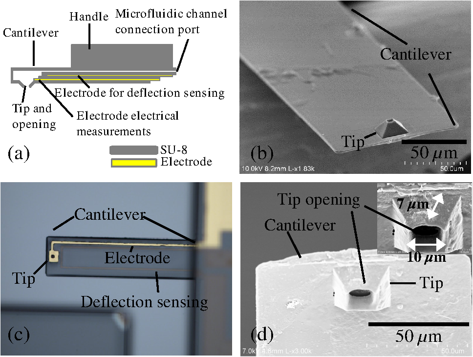 The cantilever described herein and shown in Fig. 1 includes a microfludic channel with an electrode near the tip. A cross-sectional drawing is shown in Fig. 1(a) and a scanning electron microscopy (SEM) image is shown in Fig. 1(b). A force sensing mechanism [visible in Fig. 1(c)], similar to the ones previously developed by us,17,18 is included in the form of an electrode and is sandwiched between two layers of SU-8 and reaches the tip. An opening that will ultimately allow for microinjections and patch-clamp measurements is also included [Fig. 1(d)]. The tip of this initial device has an opening diameter of and a height of . The cantilever’s width is . The cantilever includes a channel of tall running from the base of the AFM device to the sharp tip. The length of the cantilever varied between 1.6 and 0.4 mm yielding devices with spring constants between 0.019 and . The holding chips were also made of SU-8 with dimensions 8-mm long, 3.3-mm wide, and 0.15-mm thick (Fig. 1). The process flow of the cantilever is schematically shown in Fig. 2. Initially, a p-type silicon on insulator (SOI) (100) wafer with a buried oxide and, for this implementation, a device layer was used. First, this wafer is thermally oxidized creating a 200 nm oxide, which is used as a masking layer. The size of the opening and the thickness of the device layer Si will determine the height of the tip and the diameter of the opening. Next, the oxide is etched [Fig. 2(a)] until the Si layer is reached. Potassium hydroxide (KOH) is used to etch the Si and forms a pit which is used as a mold that defines the tip [Fig. 2(b)]. KOH is utilized to get a tapered tip and to better define the height of the tip, because it will stop etching on the (111) plane, thereby ensuring an accurate and reproducible tip. As the tip is etched, a 54-deg angle is created from the edge of the mask opening. The etch stops on the buried oxide and creates what will eventually become the tip opening. Other methods of etch, or DRIE, would not give the tapered profile and precise tip opening needed for this structure. Fig. 2The fabrication process. The letters correspond to specific fabrication steps described in detail the text. 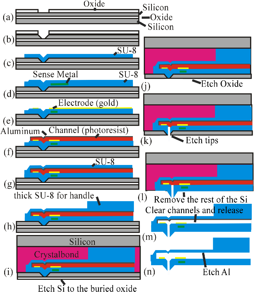 Several layers of SU-8 are used to define and create the shank, base, microfluidic channel, and metal isolation. The metals are utilized for sensing. Chrome and gold (Cr/Au/Cr) are used both for the patch clamp electrode with thickness and the deflection sensor with thickness . Standard photolithography and liftoff processes are used for fabricating the metal layers. Three layers of thick SU-8 2002 (MicroChem, Westborough, Massachusetts) are used to define the flexible shank, fluidic channel, and tip, and a thick (after curing) layer of SU-8 2050 (MicroChem) is used to create the more rigid base/handle and microfluidic connectors. To achieve these thicknesses, SU-8 2002 is spun at 2000 revolutions per minute (RPM) and SU-8 2050 is spun at 1000 RPM, and every layer is fully cured before adding the next layer. After fabrication of the mold, the first layer of SU-8 2002 is spun and patterned [Fig. 2(c)]; the deflection sensing element is deposited and patterned [Fig. 2(d)]; another layer of SU-8 is spun [Fig. 2(d)] and the electrode is evaporated [Fig. 2(e)]; an photoresist is spun to create the channel and aluminum (Al) is evaporated or sputtered and defined before and after the photoresist to isolate the photoresist from the solvents in the uncured SU-8 [Fig. 2(f)]; the top layer of SU-8 is spun [Fig. 2(g)]; finally, thick SU-8 2050 is spun to create the device handle [Fig. 2(h)]. Once the device has been defined on the surface of the SOI wafer, the wafer is bonded to a second wafer using Crystalbond [Fig. 2(i)]. The handle Si of the SOI wafer is mostly removed with a wet etch (hydrofluoric, nitric, and acetic acid), and finished with dry etching using xenon difluoride () [Fig. 2(j)]. The combination of wet and dry etchings served two purposes. First, wet etching is much faster and more cost effective than the dry etching. Second, we were concerned about heat dissipation for fast dry etching of the handle wafer. Terminating with dry etching at the end was necessary because wet etching would attack the buried oxide. Once the handle wafer was significantly removed, the final Si removal was done with the . This exposes the buried oxide layer, which is subsequently removed by buffered oxide etch (BHF) [Fig. 2(k)]. The SOI device layer Si is used as a mask for the tip, whereas plasma is used to etch through the tip’s SU-8 reaching to the photoresist-defined microfluidic channel [Fig. 2(l)]. This creates a mass produced, well-defined vertical fluidic channel into the horizontal fluidic channel. Finally, the device layer Si is removed using , leaving the polymer devices attached to a carrier wafer using Crystalbond [Fig. 2(m)]. The devices are soaked in acetone to remove the Crystalbond and the resist from the microfluidic channel [Fig. 2(n)]. After rinsing in isopropyl alcohol, the devices are separated and Al is removed [Fig. 2(n)]. Finally, the microfluidics and electrical connections are made. To test the device, the cantilever was electrically connected with thin insulated wire that was stripped at the ends [Fig. 3(a)]. Conductive epoxy was used to glue the wires on the electrical pad. The cantilever was cured in an oven for several minutes. Then, it was glued on a glass slide using polydimethylsiloxane (PDMS) and left to dry. PDMS was used to insulate the chip’s top part, the pads, and the wires from possible exposure to the liquid environment. Fig. 3(a) Optical picture of the cantilever. The wire was glued using conductive epoxy. The cantilever was insulated with PDMS and glued on a glass slide. Then, the glass slide with the cantilever is attached to a micromanipulator facing downward. The wire is connected with clip to establish the electrical contact. (b) Cantilever is immersed in saline solution. (c) Two fixed electrodes immersed in saline solution. (d) Resistance between the cantilever and electrode [shown in (b)] is compared with a resistance between two electrodes immersed in saline solution [shown in (c)]. 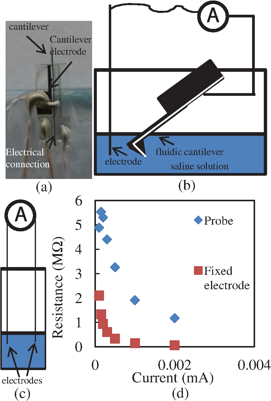 In order to conduct a preliminary electrical characterization, we immersed the cantilever in a saline solution. We connected a Keithley 2400 source meter to an electrode and the cantilever, as shown in Fig. 3(b). Extra care was given to ensure that only the cantilever is immersed, although the entire device was insulated. We then measured the resistance between the electrode wire and the cantilever through the saline solution by varying the current and recording the resistance value [Fig. 3(b)]. We repeated the same measurements in saline solution with two similar wire electrodes and compared the results [Fig. 3(c)]. The experimental results, as shown in Fig. 3(d), demonstrate that the electrode residing inside the tip opening is exposed so that the current can flow between the electrode in the solution and the electrode in the cantilever yielding a resistance . The resistance values with current are comparable with the ones obtained when a wire is used instead of a cantilever, as in Fig. 3(d). While in this preliminary effort the fabricated cantilever includes a tip with an opening diameter of , the opening can be further miniaturized to submicron dimensions for patch clamping and other nanotechnology applications. The height of the cantilever tip is set by the thickness of the SOI layer. The tip diameter is set by the initial masked opening and the thickness of the SOI layer. By adjusting the thickness and the initial opening, one can modify the fluidic hole diameter. Ultimately, this device can be used for agent delivery, electrophysiological measurements, and cell stiffness (elastography) measurements, among other applications. This technique can also be modified to create reliable microfluidic chip connectors to outlet and inlet tubes. Generally, it is easier to fabricate connections “in-plane” rather than “out of plane” of the wafer. However, it is more desirable to establish “out of plane” connections for microfluidic systems. This fabrication process can be used to create “out of plane” connections to microfluidic systems. AcknowledgmentsThe authors thank Dr. Weibin Zhu, Dr. Tao Li, Dr. Codrin Cionca, Katharine Beach, Prof. Ning Xi, Dr. Chanmin Su, and Dr. Flicker for their help and support. This research was funded by National Science Foundation grant number 1248339 (A.G.) and National Institutes of Health grant number GM084520 (A.G.). ReferencesE. NeherB. SakmannJ. H. Steinbach,
“The extracellular patch clamp: a method for resolving currents through individual open channels in biological membranes,”
Pflügers Arch., 375
(2), 219
–228
(1978). http://dx.doi.org/10.1007/BF00584247 PFLABK 0031-6768 Google Scholar
F. J. SigworthK. G. Klemic, Biological Membrane Ion Channels, 571
–593 Springer, New York
(2007). http://dx.doi.org/10.1007/0-387-68919-2 Google Scholar
B. PriestG. J. KaczorowskiM. L. Garcia,
“Ion channel modulators: new targets and new indications for old targets,”
Curr. Opin. Drug Discovery Dev., 9 587
–594
(2006). CODDFF 2040-3437 Google Scholar
Y. ZhangL.-C. Yu,
“Single-cell microinjection technology in cell biology,”
BioEssays, 30
(6), 606
–610
(2008). http://dx.doi.org/10.1002/(ISSN)1521-1878 BIOEEJ 0265-9247 Google Scholar
O. P. HamillDon W. McBride Jr.,
“Induced membrane hypo/hyper-mechanosensitivity: a limitation of patch-clamp recording,”
Annu. Rev. Physiol., 59 621
–631
(1997). http://dx.doi.org/10.1146/annurev.physiol.59.1.621 ARPHAD 0066-4278 Google Scholar
R. D. Pineret al.,
“’Dip-pen’ nanolithography,”
Science, 283
(5402), 661
–663
(1999). http://dx.doi.org/10.1126/science.283.5402.661 SCIEAS 0036-8075 Google Scholar
K. Costa,
“Single-cell elastography: probing for disease with the atomic force microscope,”
J. Dis. Markers, 19
(2–3), 139
–154
(2004). http://dx.doi.org/10.1155/2004/482680 0278-0240 Google Scholar
S. Iyeret al.,
“Atomic force microscopy detects differences in the surface brush of normal and cancerous cells,”
Nat. Nanotechnol., 4 389
–393
(2009). http://dx.doi.org/10.1038/nnano.2009.77 1748-3387 Google Scholar
S. E. Crosset al.,
“Nanomechanical analysis of cells from cancer patients,”
Nat. Nanotechnol., 2 780
–783
(2007). http://dx.doi.org/10.1038/nnano.2007.388 1748-3387 Google Scholar
S. Suresh,
“Nanomedicine: elastic clues in cancer detection,”
Nat. Nanotechnol., 2 748
–749
(2007). http://dx.doi.org/10.1038/nnano.2007.397 1748-3387 Google Scholar
Q. S. Liet al.,
“AFM indentation study of breast cancer cells,”
Biomed. Biophys. Res. Commun., 374 609
–613
(2008). http://dx.doi.org/10.1016/j.bbrc.2008.07.078 BBRCA9 0006-291X Google Scholar
Y. Guet al.,
“High-resolution scanning patch-clamp: new insights into cell function,”
FASEB, 16
(7), 748
–750
(2002). http://dx.doi.org/10.1096/fj.01-1024fje FASMDG 0098-2385 Google Scholar
A. Meisteret al.,
“FluidFM: combining atomic force microscopy and nanofluidics in a universal liquid delivery system for single cell applications and beyond,”
Nano Lett., 9
(6), 2501
–2507
(2009). http://dx.doi.org/10.1021/nl901384x NALEFD 1530-6984 Google Scholar
K. W. C. Laiet al.,
“Development and testing of nano robot end effector for cell electrophysiology and elastography studies,”
in 2011 11th IEEE Conference on Nanotechnology (IEEE-NANO),
1066
–1069
(2011). http://dx.doi.org/10.1109/NANO.2011.6144645 Google Scholar
P. N. MinhT. OnoM. Esashi,
“Nonuniform silicon oxidation and application for the fabrication of aperture for near-field scanning optical microscopy,”
Appl. Phys. Lett., 75
(26), 4076
–4078
(1999). http://dx.doi.org/10.1063/1.125541 APPLAB 0003-6951 Google Scholar
G. Genoletet al.,
“Soft, entirely photoplastic probes for scanning force microscopy,”
Rev. Sci. Instrum., 70
(5), 2398
–2401
(1999). http://dx.doi.org/10.1063/1.1149767 RSINAK 0034-6748 Google Scholar
A. GaitasS. GianchandaniW. Zhu,
“A piezo-thermal probe for thermomechanical analysis,”
Rev. Sci. Instrum., 82 053701
(2011). http://dx.doi.org/10.1063/1.3587624 RSINAK 0034-6748 Google Scholar
W. Zhuet al.,
“A colorimetric receptor combined with a microcantilever sensor for explosive vapor detection,”
Appl. Phys. Lett., 98 123501
(2011). http://dx.doi.org/10.1063/1.3567011 APPLAB 0003-6951 Google Scholar
|


