|
|
1.IntroductionThe large amount of carbon dioxide () produced by highly developed industries not only results in serious air pollution and health problems, but also causes ocean acidification and decreases the survival rate of fry in aquaculture.1,2 Therefore, the development of a system for real-time detection of concentrations in aquaculture has become a very important research issue. Optical analysis and gas chromatography are the two main methods adopted for conventional gas detection. Although conventional detectors have high sensitivity and accuracy, their high fabrication costs, large dimensions, low potential for batch fabrication, and lack of real-time monitoring functions can limit their applications. To solve these problems, many publications have focused on the development of ion-sensitive field effect transistor (ISFET)-based ion-selective sensors, and various polymeric membranes and ionophores have been proposed over the past three decades.3–14 However, the extreme small sensing area of ISFETs usually results in an unacceptable hysteresis voltage and packaging problems. To overcome these disadvantages of ISFETs, this study has adopted an extended gate field-effect-transistor (EGFET) structure to isolate the FET from the chemical and biological environments.15–17 The sensing membrane is deposited on the end of the signal line extended from the FET gate electrode. The EGFET configuration presents many advantages, including light insensitivity, ease in packaging, and flexibility of the shape of the extended gate area. However, most ISFET- or EGFET-related devices have used a separate commercial macroreference electrode (RE) to provide a stable potential in the electrochemical measurement system. This requirement restricts their convenience and applicability for electrochemical ion sensing measurements. In 2003, our previous research developed an all solid-state unpackaged planar Ti/Pd/Ag/AgCl/KCl-gel microreference electrode () with a very high stable potential (drift voltage over 30 min), very small offset voltage (0.45 mV), and near-total insensitivity to pH value or concentration (less than 2-mV variation from pH4 to pH10 and less than 0.25 mV over a KCl concentration range from 0.1 to 0.6 M).18,19 However, the potential stability of the unpackaged Ti/Pd/Ag/AgCl/KCl-gel degraded after it was in operation for more than 1 h because the ions of the saturated KCl-gel gradually diffused into the sample solution. To effectively seal the agarose-stabilized KCl-gel layer and simultaneously reserve a miniature liquid junction on the planar Ag/AgCl , we developed a novel chip-level packaging technique in our previous research.20 Two wafers were used in that research: the first was referred to as the “KCl-gel cap sealing wafer” (with a micromachined cavity filled with KCl-gel and a microliquid-junction aperture) and the second wafer was denoted as the “Ti/Pd/Ag/AgCl quasireference electrodes (QREs) wafer.” The performance of the proposed Ti/Ag/AgCl/KCl-gel planar solid-state reference electrodes is very close to commercial . In this paper, the implemented EGFET-based microsensor and Ti/Ag/AgCl/KCl-gel are packaged on a printed circuit board (PCB) substrate to form a miniaturized sensing system. The total dimension of the proposed sensing system is only , which is approximately 30 times less than a conventional sensing system (which includes a commercial Ag/AgCl RE). All the fabrication processes presented in this study for the EGFET and are compatible with IC and microelectro-mechanical systems (MEMS) technology. Many sensing characteristics of the implemented EGFET-based sensing system will be discussed in this research including sensitivity, sensing linearity, hysteresis voltage, and lifetime. 2.Design and FabricationAs Fig. 1 shows, the EGFET was designed with a channel width/length ratio. The areas of the designed extended gate, source, and drain electrodes are equal to , and their distances from the FET active area are the same (1 mm). To implement a high-performance EGFET-based microsensor, an extended gate with large area can provide a more uniform surface onto which to coat the solid electrolyte membrane and gas permeable membrane. In addition, a longer distance between the sensing area and the FET electrode areas can facilitate the packaging process. Fig. 1(a) Top-view layout and (b) cross-sectional structure of the presented extended gate field-effect-transistor (EGFET)-based carbon dioxide () microsensor. 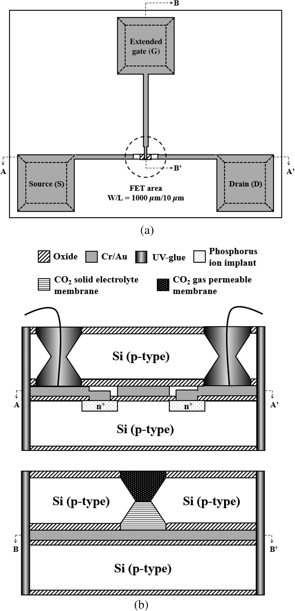 2.1.Fabrication of the Extended Gate Field-Effect-Transistor-Based Carbon Dioxide MicrosensorAll of the manufacturing processes that were adopted to implement a low-hysteresis and high-linearity EGFET-based microsensor are compatible with standard integrated-circuit planar technology and are very suitable for mass production. The complete fabrication process only requires three photomasks. Three thin films comprised the full structure of the proposed EGFET-based microsensor including one insulator layer (), three electrodes (Cr/Au) and one solid electrolyte membrane/gas permeable membrane. A schematic illustration of the main processing steps is shown in Fig. 2 and is briefly described as follows:
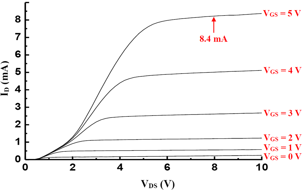
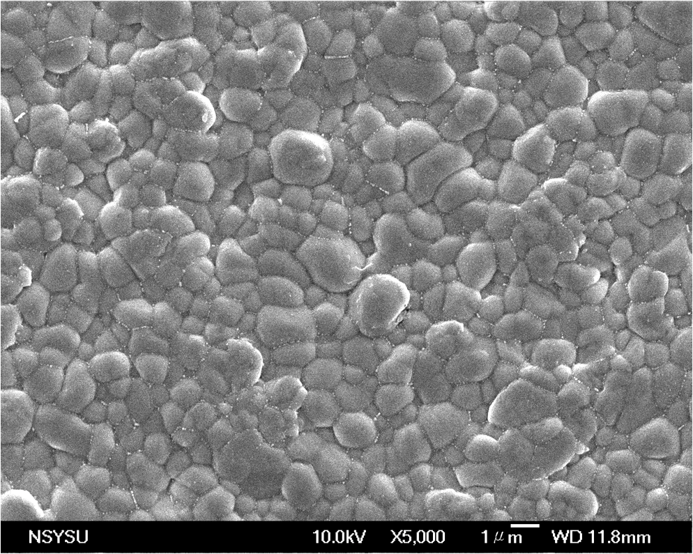
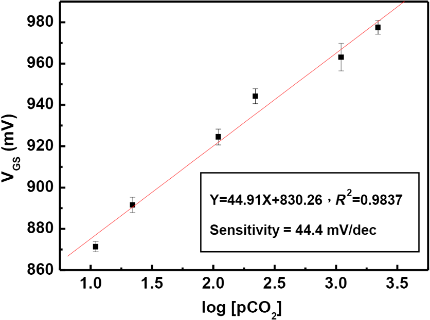
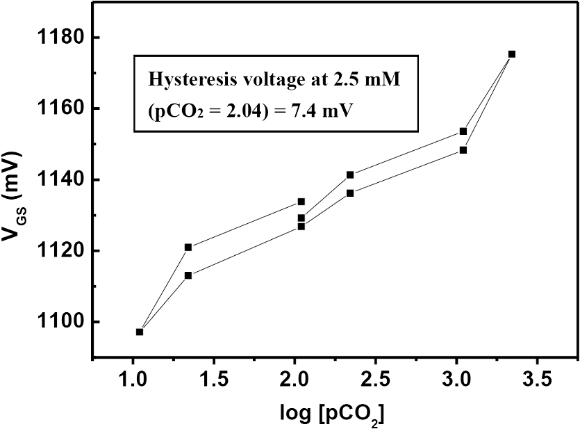
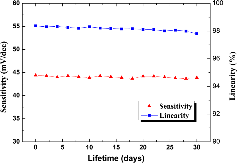
Fig. 2Main fabrication processing steps of the EGFET-based microsensor. (a) Pattern oxide layer for the phosphorus ion implantation mask, (b) form the source/drain regions of the EGFET device, (c) regrow a new oxide layer, (d) define the source/drain/gate electrodes, (e) wire bond enameled wires to the electrode pads, (f) assemble a package chip on the EGFET chip, (g) coat the gas permeable membrane/ solid electrolyte membrane onto the EGFET sensing area. 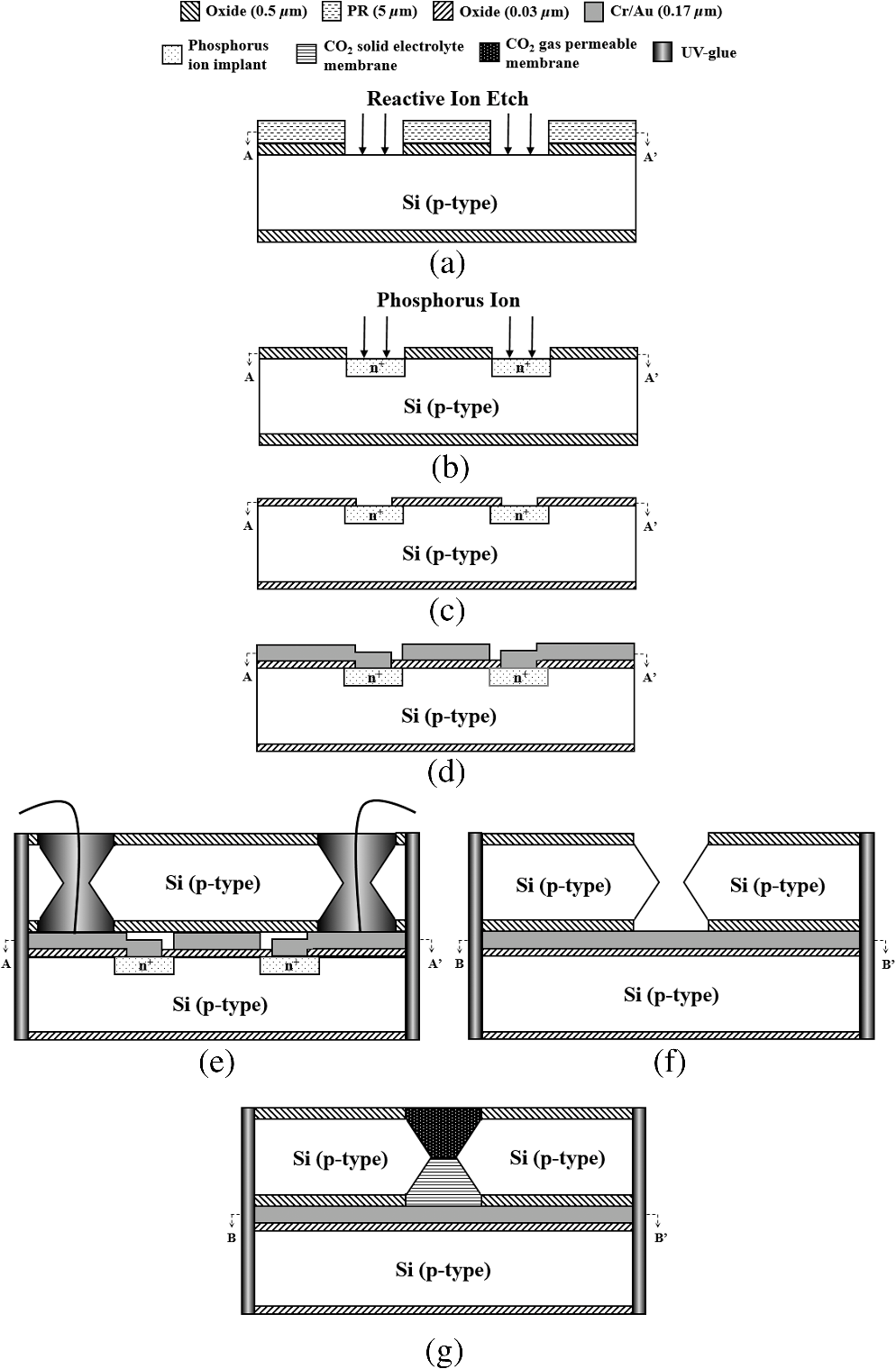 2.2.ReagentsPolymer vinyl alcohol was purchased from Fluka. Sodium bicarbonate (), sodium chloride (NaCl), tetrahydrofuran (THF), Bis(2-ethylhexyl) Sebacate (DOS), and carbonic anhydrase (from bovine erythrocytes) were purchased from Alfa Aesar. Silicone rubber (RTV 3440) and valinomycin were purchased from Dow Corning Co. Ltd., Midland, Michigan, and Sigma-Aldrich, respectively. 2.3.Fabrication of the Ti/Ag/AgCl/KCl-Gel Microreference ElectrodeAs Fig. 3(a) shows, a thin film Ti/Ag/AgCl QRE was developed for this work where the titanium layer is used to improve surface adhesion. In the fabrication of the QRE, integrated circuit processing technology and lift-off techniques were utilized to deposit and pattern the multilayer metals. The Ti (60 nm) layer was electron-gun evaporated first in sequence and without breaking the vacuum to avoid oxidation of the titanium film. Next, a Ag layer was DC-sputtered onto the Ti layer. Our research20 determined that a Ag layer worked reasonably well. Chlorination of the silver electrodes was carried out electrochemically in a 0.1 M HCl (J. T. Baker) solution by applying either a constant voltage of 1.0 V or a constant current of several tenths of mA. Therefore, chlorination of the silver surface proceeded in the constant current mode using a current density of for 10 min. Fig. 3Main fabrication processes of the chip-level packaged microreference electrode (): (a) the process of dispensing the conducting-epoxy layer and binding the silver wire, (b) the process of dispensing the saturated KCl-gel and (c) the UV-glue sealing and bonding process. 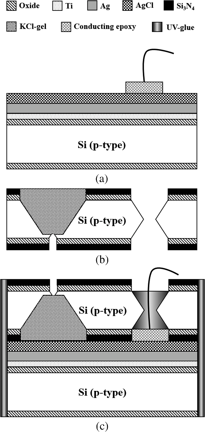 The cross-sectional diagram of the KCl-gel cap sealing wafer is displayed in Fig. 3(b). The two bulk-micromachined silicon cavities were designed for the conducting-epoxy/UV-glue encapsulated electrical conduction wire and the KCl-gel sealing cap, respectively. The window size of the KCl-gel trapezoid cavity is , and the corresponding KCl-gel injection volume in the cavity is . However, the dimension of the liquid-junction aperture is fixed at , and the window size of the conducting-epoxy/UV-glue sandglass-shaped cavities on both sides of the wafer was kept constant at . To enhance the endurance of the Ti/Ag/AgCl QRE against contamination caused by the sample solution and to improve its ability to provide a constant reference potential free from the effects of changing ion concentration, an agarose-supported KCl-gel membrane was employed. The KCl-gel membrane not only ionically bridges between the AgCl layer and the sample solution, but also supplies a stable and sufficient concentration to the AgCl/KCl-gel/sample solution interfaces to achieve a stable junction potential. In our experiments, the 2 wt% agarose powder was dissolved in a saturated 3 M KCl solution, heated to the agarose melting temperature (150°C), mixed thoroughly and cooled to the gelling temperature (60°C–70°C) prior to dispensation into the “KCl-gel filling cavity” as shown in Fig. 3(a) using the syringe method. Finally, as Fig. 3(c) shows, a commercial UV-glue was used to seal and bond the KCl-gel filled chip and the wire-connected Ti/Ag/AgCl chip in an ultraviolet (UV) exposure system. The dimensions of the two chips are large enough to be manually aligned and assembled on a microscope working stage. To avoid any melting or vaporization of the KCl-gel, the curing temperature of the UV-glue was controlled at under 25°C–30°C. The fabrication yield of the sealing and packaging processes mentioned above is approximately 45% in a lab environment, and the total dimensions of the implemented chip-level packaged planar Ti/Ag/AgCl/KCl-gel module are equal to , which is approximately 250 times less than the traditional commercial Ag/AgCl RE ( and ). 3.Results and DiscussionsAs shown in Fig. 4(a), the EGFET-based microsensors and the planar Ti/Ag/AgCl/KCl-gel reference electrode were combined together on a PCB substrate. To facilitate the packaging and testing processes, we produced an array of five EGFET-based microsensors with the same design on one die (), and their source electrodes are connected together as a common source. For each measurement presented in this research, the common source connecting wire was attached to electrical ground. The drain electrodes of the five EGFET-based microsensors were not connected together and have individual connecting wires; hence, the total number of connecting wires on the chip is six (one common source and five drains). This study used a commercial semiconductor parameter analyzer (Agilent B1500A) to characterize the transistor and microsensor in standard testing solutions. The test setup utilized in this study is shown in Fig. 4(b). The microsensor was immersed into the testing solution. The reference electrode provides a constant voltage in the testing solution and serves as a gate potential to the EGFET. Different ion concentrations will affect the absorbed charge on the ISM surface, and the results appear as various gate voltages on the EGFET. Fig. 4(a) Photograph of the encapsulated EGFET-based carbon dioxide () microsensor with the planar Ti/Ag/AgCl/KCl-gel microreference electrode (). (b) Schematic diagram of the testing setup. 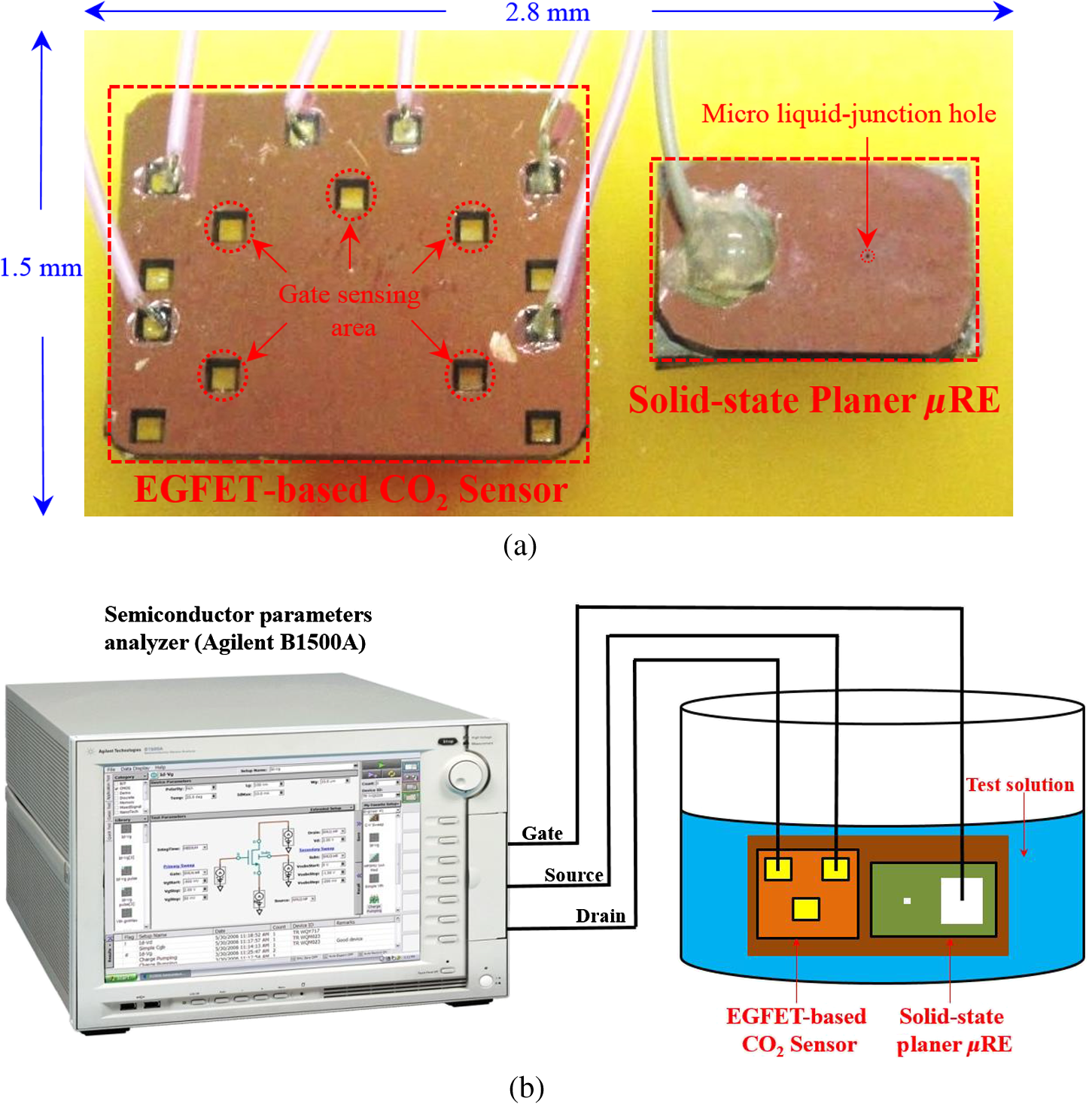 3.1.Characterization of the Extended Gate Field-Effect-Transistor DeviceTo examine the basic electrical characteristics of the fabricated EGFET (with a channel width/length ratio), the EGFET output current/voltage and gate leakage characteristics were measured with an Agilent B1500A semiconductor parameter analyzer. Figure 5 shows the drain current versus drain voltage () in the implemented EGFET. In this research, 20 EGFET dies were implemented and characterized. As the gate and drain electrodes are biased at 5 and 8 V, respectively, the drain current of presented 20 EGFETs (with same rectangular channel design) ranges from 8.3 to 8.4 mA. The variation of the drain current is not obvious. Moreover, as the drain and gate electrodes biased at other conditions, the variation of the drain current of presented 20 EGFETs (with same rectangular channel design) is also very small (about 0.1–0.2 mA). 3.2.Characterization of the Planar Ti/Ag/AgCl/KCl-Gel Reference ElectrodeFigure 6 shows the scanning electron microscope surface micrographs of the AgCl layer. The porosity of the AgCl layer can have a large influence on the impedance of the , and a higher porosity in the top AgCl layer results in a greater possibility of directly exposing the underlying Ag layer to the KCl-gel solid-state electrolyte, which would cause interference noise through redox reactions. To avoid this situation, the electrochemically chlorinated AgCl layer must contain no gross pores. The chlorination conditions chosen in this study (current density of for 10 min) were able to produce a AgCl layer with a well-controlled grain size of approximately and with nearly zero porosity. The stabilities of the voltage potentials for the unpackaged planar Ti/Ag/AgCl QRE and the chip-level packaged and unpackaged planar Ti/Ag/AgCl/KCl-gel were characterized by a potentiometric analysis. The analysis was accomplished by measuring the open circuit potential (OCP) with a two-electrode system in 0.01 M KCl aqueous solution at 25°C over 30,000 s. To test the performance of our fabricated electrodes when used as reference electrodes, the fabricated electrodes were given the role of RE and the commercial Ag/AgCl electrode was the WE in our OCP measurement assembly. Figure 7(a) shows the OCP variations of chip-level packaged planar Ti/Ag/AgCl/KCl-gel with of KCl-gel volume compared with a commercial Ag/AgCl RE over 30,000 s of testing time. The measured potential drift of the planar Ti/Ag/AgCl (2.9 mV over 30,000 s) is approximately equal to that of the commercial Ag/AgCl RE (1.6 mV over 30,000 s). Moreover, the offset voltage of the planar Ti/Ag/AgCl () is smaller than that of the commercial Ag/AgCl RE (). Fig. 7(a) Potentiometric and (b) impedance analyses of the commercial Ag/AgCl RE and the planar Ti/Ag/AgCl/KCl-gel microreference electrode (). (c) The sensitivity to changes in concentration for Ti/Ag/AgCl QRE and the planar Ti/Ag/AgCl/KCl-gel . 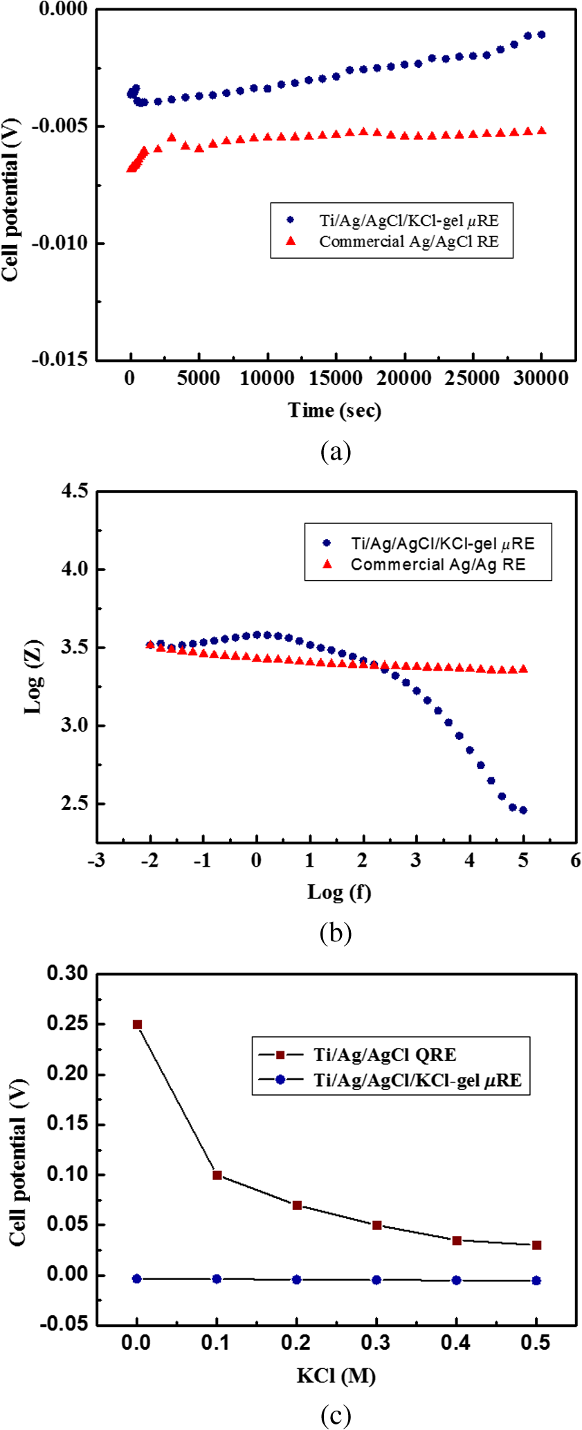 The impedance of a is determined by the resistance of its isolation junction (the liquid junction aperture), which separates the internally filled aqueous KCl or KCl-gel from the sample electrolyte. We built a three-electrode electrochemical cell to measure the impedance and phase shift of three chip-level packaged Ti/Ag/AgCl/KCl-gel at 25°C. The three-electrode cell is composed of a WE (which is our ), a platinum CE and a commercial Ag/AgCl RE. The measured absolute values of the impedances are plotted as a function of frequency. The scanning frequency of the small amplitude sinusoidal excitation signal ranges from 0.01 to 100 kHz. Figure 7(b) shows that the impedance measured at 1 kHz of the solid-state planar is approximately 3.223 kΩ, which is smaller than that of the commercial Ag/AgCl RE (approximately 3.377 kΩ). A slow diffusion of the filled solution through this junction is necessary for proper electrode operation. Unfortunately, slower diffusion flow requires a more restricted flow path, and the resistance of the electrolyte along the path will increase. The small impedance of the RE means that little compensation potential is required for the WE and CE. In short, there is a fundamental trade-off between electrode impedance and leakage rate. The qualification of an electrode to be used as a reference electrode requires not only it can provide a stable chemical potential while immersed in the testing solution, but also it has to provide a stable potential against any variations in concentration in the testing solution. Figure 7(c) shows the Ti/Ag/AgCl QRE and the Ti/Ag/AgCl/KCl-gel cell potentials calibrated against the concentration. The potential variation of presented planar Ti/Ag/AgCl/KCl-gel is only about over the range of 0–0.5 M concentration of ion. However, as shown in Fig. 8, the presented sensor demonstrates a high sensitivity (). Therefore, the influence of final sensitivity testing results on the potential variation of presented planar reference electrode is only about 0.9–1.6% (, ). Therefore, the proposed can provide a nearly stable potential against ion concentration of testing solution. 3.3.Characterization of the Extended Gate Field-Effect-Transistor-Based MicrosensorIn the development of a sensing microsystem, microsensing elements with high sensitivity and high sensing linearity can facilitate the design and reduce the fabrication cost of the signal processing circuits. Figure 8 shows the measured gate voltage of the fabricated EGFET-based microsensor in a standard testing solution with six different concentrations (0.25 to 50 mM). Each testing point represents the test data from five microsensors of the same design. As shown in Fig. 8, very high sensing linearity (98.4%) and high sensitivity () are obtained in this study. According to the experimental results, the fabricated EGFET-based microsensor has a response time of 100 s, and its output signal reaches a stable value within 5 min. To investigate the selectivity of the proposed sensing system, this paper also measured the gate voltage of the fabricated EGFET-based microsensor in a standard testing solution with six different dissolved concentrations (0.25 to 50 mM). The measured sensitivity of the proposed sensing system for varied dissolved oxygen () concentrations is only , which is much less than that for gas (). Based on the theory, and the other gas molecules in aqueous solution can diffuse through the gas permeable membrane into the solid electrolyte membrane. However, only molecules can generate a more obvious reaction with the solid electrolyte membrane and a resulting pH change can be detected by the EGFET microsensor. Hysteresis is a very important parameter in microsensors that must be characterized; however, few previous studies have performed the necessary investigations. Low-hysteresis voltages indicate a reliable and repeatable microsensor response. Figure 9 presents a hysteresis characterization of the fabricated EGFET-based microsensor. The hysteresis voltages were measured using a standard testing solution with concentration altered every 20 m in the sequence of 2.5, 5, 25, 50, 25, 5, 2.5, 0.5, 0.25, 0.5, and 2.5 mM. A very small hysteresis voltage (7.5 mV) was measured at 2.5 mM. The long-term stability (lifetime) of the implemented EGFET-based microsensor (with the planar Ti/Ag/AgCl/KCl-gel ) was also investigated in this work. During the lifetime analysis, the sensor chip is immersed into a standard chloride testing solution with six different concentrations (in the range 0.25–50 mM), and each concentration was tested for 5 min. The long-term stability measurement result is shown in Fig. 10. The total testing time over a single day was approximately 25 min, and the sensor chip was stored under dry conditions at room temperature in the periods between tests. During 30 days of measurement, the implemented EGFET-based microsensor (with the planar Ti/Ag/AgCl/KCl-gel ) demonstrated a very stable sensitivity (varied only from 43.7 to ) and linearity (varied from 97.8% to 98.37%); hence, the lifetime of the presented EGFET-based sensor is more than 30 days. Finally, as Table 1 shows, we compared the five sensing characteristics (sensitivity, sensing linearity, linear range, hysteresis voltage, and response time) addressed in this study in the optimum compositions with those in the previous literature.21–23 The implemented EGFET-based sensing system with a packaged presents the highest sensitivity, the widest linear range, and the fastest response time in those microsensors. Substantially, the EGFET-based microsensor developed in this study demonstrates a moderate sensitivity (), a very high sensing linearity (98.37%), a wide linear range (0.25–50 mM) and a very low-hysteresis voltage (7.5 mV). Table 1Comparison of this research with the previous literatures of CO2 microsensors. 4.ConclusionIn this paper, the design, fabrication, and performance characterization of a high-performance EGFET-based sensor integrated with a planar Ti/Ag/AgCl/KCl-gel reference electrode were presented. All of the fabrication processes are compatible with IC and MEMS technologies. The EGFET-based microsensor has a rectangular gate ( channel width/length ratio), its extended gate area is coated with a solid electrolyte membrane and a gas permeable membrane. The device demonstrated a very high sensitivity () and very high sensing linearity (98.37%), with sensing concentrations ranging from 0.25 to 50 mM. Furthermore, a very small hysteresis voltage (7.5 mV) was obtained over the cycle 2.5 mM–5 mM–25 mM–50 mM–25 mM–5 mM–2.5 mM; this result was achieved by improving the surface planarization and enlarging the sensing area of the EGFET to . AcknowledgmentsThe authors would like to thank the National Science Council and National Sun Yat-sen University of the Republic of China, Taiwan, for financially supporting this research under Contract Nos. NSC 101-2221-E-110-080, NSC 102-2221-E-110-078, and EI-28-05-10-101. The authors are indebted to the National Nano Device Laboratories (NDL) in Taiwan for their assistance in providing access to their processing facilities. ReferencesH. B. Glasgowet al.,
“Real-time remote monitoring of water quality: a review of current applications, and advancements in sensor, telemetry, and computing technologies,”
J. Exp. Mar. Biol. Ecol., 300
(1–2), 409
–448
(2004). http://dx.doi.org/10.1016/j.jembe.2004.02.022 JEMBAM 0022-0981 Google Scholar
N. W. T. Quinnet al.,
“Use of environmental sensors and sensor networks to develop water and salinity budgets for seasonal wetland real-time water quality management,”
Environ. Modell. Softw., 25
(9), 1045
–1058
(2010). http://dx.doi.org/10.1016/j.envsoft.2009.10.011 EMSOFT 1364-8152 Google Scholar
P. Bergveld,
“Development of an ion-sensitive solid-state device for neurophysiological measurements,”
IEEE Trans. Biomed. Eng., BME-17
(1), 70
–71
(1970). http://dx.doi.org/10.1109/TBME.1970.4502688 IEBEAX 0018-9294 Google Scholar
S. WakidaM. YamaneK. Hiiro,
“A novel Urushi matrix chloride ion-selective field effect transistor,”
Talanta, 35
(4), 326
–328
(1988). http://dx.doi.org/10.1016/0039-9140(88)80097-3 TLNTA2 0039-9140 Google Scholar
K. Tsukadaet al.,
“Long-life multiple-ISFETS with polymeric gates,”
Sens. Actuators, 18
(3–4), 329
–336
(1989). http://dx.doi.org/10.1016/0250-6874(89)87039-8 SEACDX 0250-6874 Google Scholar
M. S. Frant,
“History of the early commercialization of ion-selective electrodes,”
Analyst, 119
(11), 2293
–2301
(1994). http://dx.doi.org/10.1039/an9941902293 ANLYAG 0365-4885 Google Scholar
P. Bergveld,
“Thirty years of ISFETOLOGY: What happened in the past 30 years and what may happen in the next 30 years,”
Sens. Actuators B, 88
(1), 1
–20
(2003). http://dx.doi.org/10.1016/S0925-4005(02)00301-5 SABCEB 0925-4005 Google Scholar
S. Ingebrandtet al.,
“Backside contacted field effect transistor array for extracellular signal recording,”
Biosens. Bioelectron., 18
(4), 429
–435
(2003). http://dx.doi.org/10.1016/S0956-5663(02)00155-0 BBIOE4 0956-5663 Google Scholar
A. BratovN. AbramovaC. Dominguez,
“Investigation of chloride sensitive ISFETs with different membrane compositions suitable for medical applications,”
Anal. Chim. Acta, 514
(1), 99
–106
(2004). http://dx.doi.org/10.1016/j.aca.2004.01.034 ACACAM 0003-2670 Google Scholar
B. H. van der SchootP. Bergveld,
“ISFET based enzyme sensors,”
Biosensors, 3
(3), 161
–186
(1987). http://dx.doi.org/10.1016/0265-928X(87)80025-1 BISSED 0265-928X Google Scholar
T. Katsubeet al.,
“Stabilization of an FET glucose sensor with the thermophilic enzyme glucokinase,”
Sens. Actuators B, 1
(1–6), 504
–507
(1990). http://dx.doi.org/10.1016/0925-4005(90)80260-7 SABCEB 0925-4005 Google Scholar
D.-S. Kimet al.,
“An extended gate FET-based biosensor integrated with a Si microfluidic channel for detection of protein complexes,”
Sens. Actuators B, 117
(2), 488
–494
(2006). http://dx.doi.org/10.1016/j.snb.2006.01.018 SABCEB 0925-4005 Google Scholar
E. M. GuerraG. R. SilvaM. Mulato,
“Extended gate field effect transistor using xerogel sensing membrane by sol–gel method,”
Solid State Sci., 11
(2), 456
–460
(2009). http://dx.doi.org/10.1016/j.solidstatesciences.2008.07.014 SSSCFJ 1293-2558 Google Scholar
C.-H. Hsiehet al.,
“Development of EGFET-based microsensors with high-sensitivity and high-linearity for dissolved oxygen and carbon dioxide detection,”
in Proc. 17th Int. Conf. on Solid-State Sensors, Actuators and Microsystems (TRANSDUCERS’ 2013) & EUROSENSORS XXVII,,
2051
–2054
(2013). Google Scholar
J. Van der Spiegelet al.,
“The extended gate chemical sensitive field effect transistor as multi-species microprobe,”
Sens. Actuators, 4 291
–298
(1983). http://dx.doi.org/10.1016/0250-6874(83)85035-5 SEACDX 0250-6874 Google Scholar
H. Eckenet al.,
“64-Channel extened gate electrode arrays for extracellular signal recording,”
Electrochim. Acta, 48
(20–22), 3355
–3362
(2003). http://dx.doi.org/10.1016/S0013-4686(03)00405-5 ELCAAV 0013-4686 Google Scholar
M. J. SchöningA. Poghossian,
“Recent advances in biologically sensitive field-effect transistors,”
Analyst, 127
(9), 1137
–1151
(2002). http://dx.doi.org/10.1039/b204444g ANLYAG 0365-4885 Google Scholar
I.-Y. HuangR.-S. Huang,
“Fabrication and characterization of a new planar solid-state reference electrode for ISFET sensors,”
Thin Solid Films, 406
(1–2), 255
–261
(2002). http://dx.doi.org/10.1016/S0040-6090(01)01783-7 THSFAP 0040-6090 Google Scholar
I.-Y. HuangR.-S. HuangL.-H. Lo,
“Improvement of integrated Ag/AgCl thin film electrodes by KCl-gel coating for ISFET applications,”
Sens. Actuators B, 94
(1), 53
–64
(2003). http://dx.doi.org/10.1016/S0925-4005(03)00326-5 SABCEB 0925-4005 Google Scholar
I.-Y. HuangS.-H. WangC.-C. Chu,
“Improved solid-state planar Ti/Pd/Ag/AgCl/KCl-gel microreference electrode by silicon cap sealing package,”
J. Micro/Nanolith., 8
(3), 033050
(2009). http://dx.doi.org/10.1117/1.3196547 JMMMGF 1932-5134 Google Scholar
J.-H. Shinet al.,
“ISFET-based differential sensors employing a low-resistance gas-permeable membrane,”
Anal. Chem., 68
(18), 3166
–3172
(1996). http://dx.doi.org/10.1021/ac960473h ANCHAM 0003-2700 Google Scholar
S.-P. Chenet al.,
“Study on a sensor based on a /Carbon electrode,”
J. Electrochem. Soc., 156
(4), 62
–66
(2009). http://dx.doi.org/10.1149/1.3072690 JESOAN 0013-4651 Google Scholar
G. Cuiet al.,
“Potentiometric sensor using polyaniline-coated pH-sensitive electrodes,”
Analyst, 123
(9), 1855
–1859
(1998). http://dx.doi.org/10.1039/a802872i ANLYAG 0365-4885 Google Scholar
BiographyChia-Hsu Hsieh received his BS and MS degrees in electrical engineering from National Sun Yat-sen University (NSYSU), Taiwan, in 2006 and 2008, respectively. Currently, he is working toward his PhD degree in the Department of Electrical Engineering of National Sun Yat-sen University. His research interests focus on ion sensors and real-time water quality monitoring microsystem. Wei-Che Hung received his BS degree in electrical engineering from National University of Tainan (NUTN), Taiwan, and his MS degree in electrical engineering from National Sun Yat-sen University (NSYSU), Taiwan, in 2011 and 2013, respectively. Po-Han Chen received his BS degree in electrical engineering from National Yunlin University of Science & Technology Tainan (NYUST), Taiwan and his MS degree in electrical engineering from National Sun Yat-sen University (NSYSU), Taiwan, in 2010 and 2012, respectively. I-Yu Huang received his MS and PhD degrees from the Department of Electrical Engineering, National Tsing-hua University (NTHU), Taiwan. Since 2003, he has devoted his professional career as an assistant professor to the Department of Electrical Engineering, National Sun Yat-sen University (NSYSU). On February 1, 2013, he became a professor at NSYSU, and his recent studies focus on the development of biomedical and electrochemical microsensors, electrostatic-drive microactuators, and RF-MEMS. |