

|
|
1.IntroductionSHARP is designed to emulate image formation in printing tools such as the ASML ADT, 3100 and 3300 scanners1,2 in terms of mask-side numerical aperture (NA), illumination and variation of the plane of incidence across the ring field. The tool’s principal application is to collect through-focus data on patterned and blank regions of extreme ultraviolet (EUV) photomasks, closely emulating a given set of imaging conditions. The data are used to study topics such as e.g., printability of defects, evaluation of repairs or three-dimensional-mask effects. SHARP’s zoneplate imaging optics match the mask-side NA values of current and future lithography generations from (wafer side) 0.25 NA at a 6 deg central ray angle (CRA) up to 0.625 NA at a 10 deg CRA. These NAs are available at different azimuthal angles covering to emulate the rotation of the plane of incidence. SHARP’s Fourier synthesis illuminator3 allows synthesizing arbitrary pupil fills. The flux on the photomask is independent of the fill pattern in use. Complementary imaging modes allow for extracting additional information from the photomask at an experiment site. In principle, with an increased sensitivity to defects, experiment sites can be found with increased speed and confidence. Previously undiscovered defects can be identified and characterized. Feedback on repairs, beyond printability in a scanner, can be provided. We have added Zernike phase contrast, differential interference contrast (DIC), cubic phase modulation, dark-field imaging and stereoscopic imaging to SHARP, most of which are widespread in visible light microscopy. The unique design of the SHARP microscope, using off-axis zoneplate lenses as imaging optics, facilitates the implementation of additional imaging modes and allows, to our knowledge, the first demonstration of DIC and Zernike phase contrast in an EUV optical system. Some of the added imaging modes have very specific illumination requirements, making SHARP’s Fourier synthesis illuminator a key component to their implementation. An overview of the SHARP microscope and detailed descriptions of its components can be found in Refs. 4 and 5. 2.Zoneplate Design and Fabrication2.1.Zoneplate DesignThe common zoneplate equation defines the ’th zone boundary for a standard zoneplate: Here, and are the imaging conjugates and and are are the distances from the object and image point to a given location in the pupil plane. The wavelength is . Figure 1(a) illustrates the geometry. Fig. 1(a) Illustration of ray path and statement of symbols used in standard zone pattern definition. (b) Illustration, showing the holographic approach to defining a zone pattern. 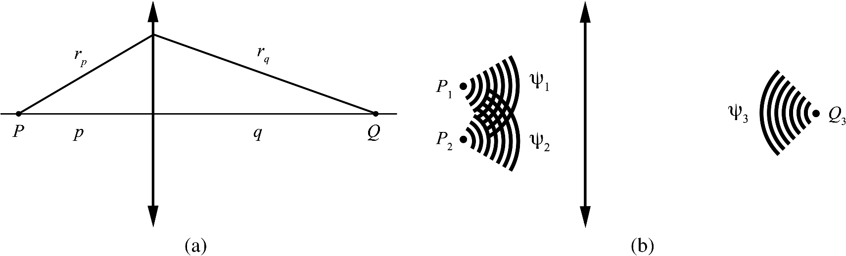 For the purposes of fabrication by electron-beam lithography, the authors have written code to generate zoneplate patterns in the graphic-database-system (GDS) format from basic inputs such as wavelength, imaging conjugates, and numerical aperture. The algorithm minimizes position errors in the output file. A web application for zoneplate design is available to the public in Ref. 6. Zoneplates can be specified via a web interface and the corresponding GDS-file can be downloaded. The site allows calculating resolution and bandwidth requirements for a given configuration and features educational content on the design, fabrication, and applications of zoneplate lenses. A holographic approach is used to define the more complex zone patterns required by some complementary imaging modes. The concept is illustrated in Fig. 1(b). For a standard zoneplate, we consider an object point and an image point . In the following example, we discuss two separate off-axis points and , imaged to the same image point . The corresponding waves in the pupil plane are defined in Eq. (2). Waves , , and can be combined in different ways in order to obtain an amplitude-only pattern that reflects the geometry given in Fig. 1(b). Two approaches are discussed as follows. The first approach is to sum the waves and calculate the intensity distribution in the pupil plane. This method is akin to the method of recording holograms in light-sensitive film. For e-beam fabrication, the resulting intensity is then binarized with a threshold intensity value to obtain a discrete zone pattern. The threshold level can be chosen to maximize a performance metric, such as diffraction efficiency into the twin first orders. The second approach is to sum the products and and threshold its imaginary part . By itself, the phase of the product in the pupil plane corresponds to a standard, off-axis zoneplate, imaging to . The latter applies to , imaging to as well. Figures 2(a) and 2(b) show function and the matching binarized pattern. Function and its binarized version are shown in Figs. 2(c) and 2(d). The plots show examples of patterns typically obtained from geometries as presented in Fig. 1(b). The equivalence of the two binarized patterns can be explained by the matching center positions of the clear zones. The resulting zoneplates will, however, be different in grating efficiencies in the diffracted orders, and may produce slightly different image qualities. Pattern optimization for nonstandard zoneplates is an ongoing topic of investigation. An important aspect to consider is the printability of different patterns in a given lithographic process. Fig. 2(a) Continuous function from Eq. (3). (b) Binarized pattern from (a). (c) Continuous function from Eq. (4). (d) Binarized pattern from (c). 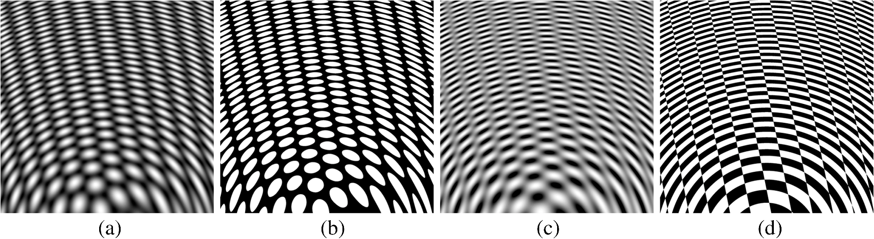 In order to create GDS-files for nonstandard zoneplates with the above approach, the continuous function or, respectively , is calculated in the pupil plane at sub-nm resolution. This is done in up to 2500 individual, tiled segments of the pupil to keep the data volume low. A contouring algorithm is applied to interpolate an outline curve for each clear zone. The outline is then approximated by a polygon, with vertices matching a tolerance of for the optical path length. The polygons from all segments are combined in a single GDS. For zoneplates that contain features smaller than 50 nm, a bias can be applied to the size of the polygons to correct for the size of the e-beam that is used for patterning. 2.2.Zoneplate NanofabricationZoneplates for the SHARP microscope are structured in silicon-nitride membrane windows on silicon chips. Figure 3(a) shows an image of SHARP’s zoneplate holder with three chips installed. Each chip is kinematically mounted, using three ruby balls that are glued into lithographically etched features on the chips and register to V-shaped grooves in the zoneplate holder. There are more than 200 zoneplates installed in the SHARP microscope. Figure 3(b) shows a magnified view of one of the zoneplate chips. Each chip holds approximately 70 zoneplates, grouped on three, 4-mm-long, silicon-nitride membranes, designed to accommodate a large number of zoneplates without compromising the robustness and flatness of the membrane. Fig. 3(a) Photographic image of SHARP’s zoneplate holder with three zoneplate chips installed. (b) Magnified image, showing one of the zoneplate chips. (c) Scanning electron microscopic image of zoneplates and holes on a chip. 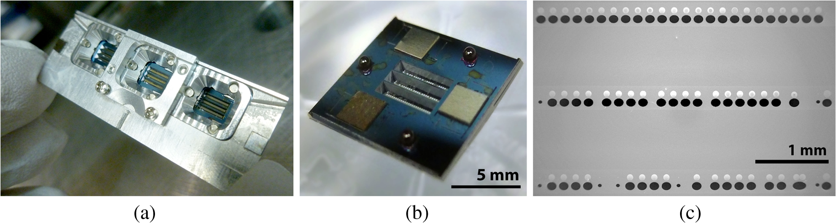 The individual chips are cut from a silicon waver with 100 nm of silicon-nitride deposited to both sides. Optical lithography is used to mask the locations of the three membranes and the holes for the ruby balls. After removing the upper silicon-nitride layer in a dry-etch process, the underlying silicon is etched all the way down to the lower silicon nitride layer to form the 3 membranes. The zone patterns are electroplated in gold using electron-beam lithography. The gold patterns are approximately 40-nm tall. To improve efficiency and to reduce the potential effects of carbon contamination, open elliptical holes are etched through the membrane for the transmitted, illuminating beam. E-beam lithography and dry etch are used to punch holes in the membrane next to each zoneplate. Figure 3(c) shows a scanning electron microscopic image of the central part of one of the chips. The image shows 68 individual zoneplates and corresponding holes for the illumination, grouped on three membranes. All zoneplates for additional imaging modes addressed in this article are designed for a 6 deg central ray angle and have a mask-side NA of 0.0825, matching the mask-side NA of the ASML 3300 scanner (0.33 wafer-side NA). 3.Zernike Phase ContrastZernike phase contrast is a microscopic technique that enhances contrast by converting phase changes from the object to intensity changes in the image. This is achieved by modifying the phase of the undiffracted light emerging from the object plane and interfering it with the scattered light from the object. The technique is named after Frits Zernike, who developed the technique in the 1930s7 and was awarded the Nobel Prize in physics for its discovery in 1953. So-called phase defects have long been a major concern in EUV mask technology.8 In particular, nanometer-scale bumps and pits in the reflective coating or the underlying substrate can shift the local multilayer properties and/or modify the optical path of adjacent portions of the reflected field. Despite their potentially strong influence on the EUV aerial image, the detection of pure phase defects can be challenging. In many cases, this type of defect shows little to no contrast in an in-focus bright-field image in the SHARP tool. See Fig. 6 for example. Zernike phase contrast is widespread in visible-light microscopy for imaging biological samples with low amplitude contrast and strong phase from the varying refractive index and optical path lengths of different materials. We recognize that this technique has the potential to enhance the contrast of phase defects and phase features on EUV masks in a similar way, thus improving the sensitivity of actinic mask imaging or inspection tools.9 Zernike phase contrast microscopy in the soft x-ray spectral range using a zoneplate lens and phase ring has been demonstrated by Schmahl et al.10 With well-collimated illumination, the required phase shift of the undiffracted light can be achieved within the zoneplate pupil, sparing the need for an additional phase-shifting element, and simplifying the design and alignment.11 Figures 4(a) and 4(b) show cartoons of a standard, off-axis zoneplate and an off-axis zoneplate for Zernike phase contrast, in comparison. To enable Zernike phase contrast, the zone pattern is phase shifted in the central part of the pupil. The transition from the unmodified outer region of the zoneplate to the phase-shifted central region is shown in the scanning electron microscope (SEM) image in Fig. 4(c). Undiffracted light from the central object plane passes through the phase-shifted region in the center of the zoneplate. Most of the scattered light from a feature or defect passes through the outer region. The two components interfere in the charge-coupled device (CCD) plane, increasing the contrast of object features having a relative phase shift. Fig. 4(a) Cartoon of a standard off-axis zoneplate. (b) Cartoon of an off-axis zoneplate for Zernike phase contrast. (c) Scanning electron microscopic image of a Zernike phase contrast zoneplate, showing the transition from the outer unmodified region of the zoneplate, to the inner phase-shifted region. 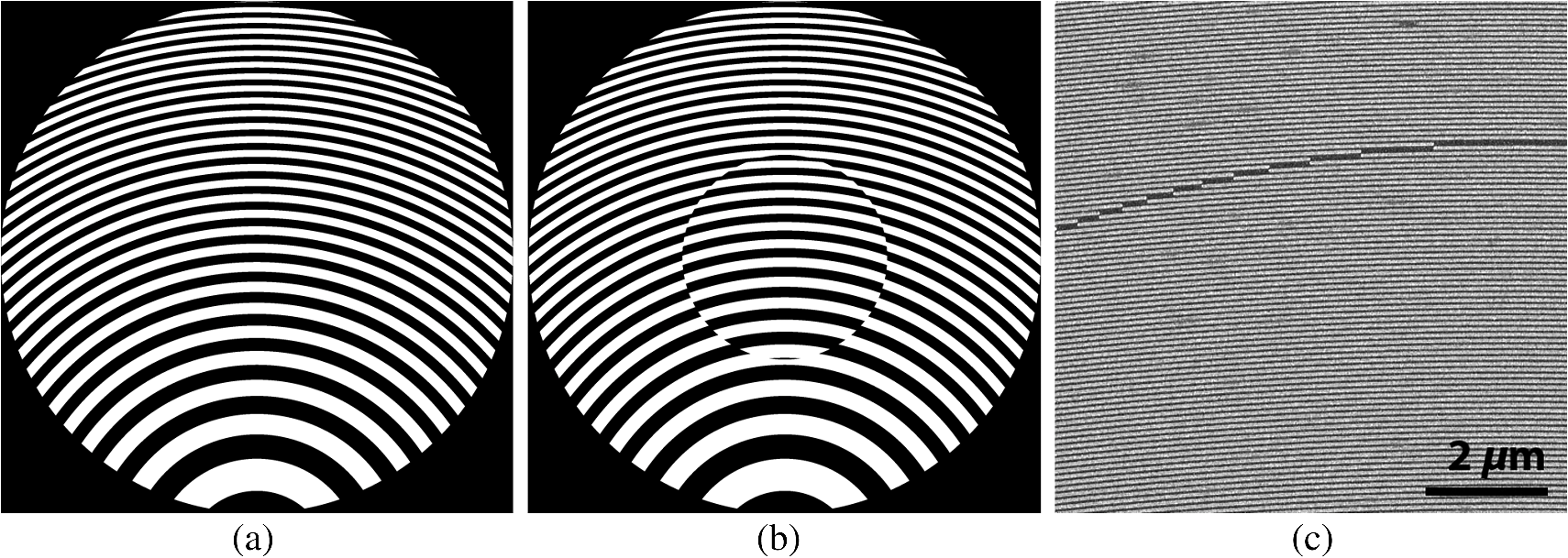 Figure 5(a) shows SHARP image data, recorded in conventional bright-field mode with a pupil fill having a partial-coherence value of 0.01 (i.e., highly coherent). The photomask imaged here was provided by the EUV team of GLOBALFOUNDRIES and manufactured at the Advanced Mask Technology Center in Dresden, Germany. It features various sizes of programmed phase defects (bumps and pits) buried under the multilayer. The image shows two large phase defects on the right clear line, resulting from programmed 12-nm-deep pits on the substrate. The larger square features are markers of the defect locations. The off-axis configuration of the SHARP microscope causes a -direction focal gradient across the image. Here, the lower defect is in focus and contrast occurs at its boundary only. The center of the pit has the same intensity level as the surrounding line. Naturally occurring defects with a more Gaussian profile and less pronounced border show significantly less contrast in focus. The upper defect on the clear line is slightly out of focus–in addition to amplitude contrast from its border, the center of the pit is brighter than the surrounding line. Depending on size and profile, phase defects typically appear bright on one side of the focus and dark on the opposite side. Displaying the full extent of intensity levels in the bright-field image [Fig. 5(a)] on a linear scale, there are no defects visible in the absorber region. Fig. 5(a) Conventional bright-field image of large phase defects, buried under the multilayer. (b) Zernike phase contrast image of the same location. (c) Magnified and individually scaled images of the defects under absorber and in clear region. (I) Bright-field on absorber. (II) Bright-field on clear line. (III) Phase contrast on absorber. (IV) Phase contrast on clear line. (d) Illustration of the pattern showing clear multilayer in white and absorber in black. Markers and phase defects under the multilayer are shown in red. 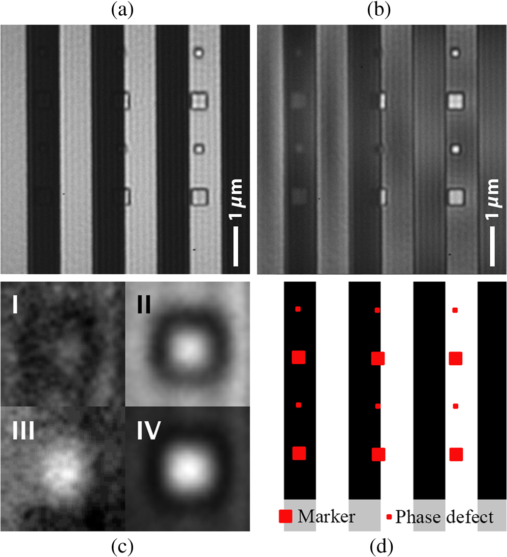 Figure 5(b) shows SHARP image data from the same location on the mask, recorded in Zernike phase contrast with the same illumination conditions. We observe a reduction in the amplitude contrast from the clear lines to the absorber, and strong phase contrast from the pit to the surrounding bright region. Displaying the image on a linear scale, defects and markers are even visible under the absorber on the left side of the image. Defect contrast is defined as half the intensity variation across a defect over the arithmetic mean intensity in the image in Eq. (5): For the defect on the clear line, Zernike phase contrast increases from 0.695 in conventional bright-field mode to 0.920. For the defect under the absorber, is increased from 0.021 to 0.100. Figure 6 shows a series of images recorded on a blank region of a photomask. The images cover a through-focus range of 800 nm below and above focus. The same phase defect on the substrate is imaged in conventional bright field (upper series) and in Zernike phase contrast (lower series). All images are recorded with an exposure time of 5 s. The images are linearly scaled with the CCD background being zero and peak intensity across the series being white. In bright-field mode, the defect shows bright below focus and dark above. In the in-focus image, the defect is not visible. In Zernike phase contrast, the defect is visible in and out of focus. Fig. 6Through-focus series of a phase defect, imaged in conventional bright-field mode (upper series) and Zernike phase contrast (lower series). 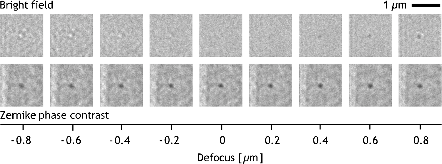 These first results show that Zernike phase contrast can significantly increase the signal from phase defects in SHARP image data, thus improving the sensitivity of the microscope. Several factors affect the appearance and observed contrast, including the magnitude of the phase shift of the central lens region, the radius in the pupil over which the phase shift is applied, the lateral size, and the phase variation across the defect being observed. Furthermore, it may be useful to apply apodization to balance the amplitudes and to optimize the contrast of the interfering elements of the field.9 Improvements in contrast will be studied for common types of phase, amplitude and combined phase and amplitude defects, and found on blank and patterned regions of EUV photomasks. 4.Differential Interference Contrast4.1.Directional Differential Interference ContrastDIC is a microscopic technique originally developed by Nomarski.12 It is sensitive both to phase and amplitude variations on small length scales in the object plane. Two images of the object are projected onto the image plane with an offset below the resolution limit. Introducing a phase to one image creates a destructive interference for regions of the image that are spatially uniform in amplitude and phase. Superimposed object points with an initial phase difference show constructive interference, with a maximum value occurring when the relative phase difference is . Variation in the amplitudes from superimposed points also affect the intensity in the image, thus contributing to contrast. DIC in the x-ray spectral range has been accomplished using twin zone plates.13 Soft x-ray microscopy in DIC with a single optical element was demonstrated by Chang et al.14 The DIC-zoneplates discussed in the following are conceptually similar to the design used in Ref 14. Figures 7(a) and 7(b) illustrate zone patterns for DIC in the - and -directions. Fig. 7(a) Cartoon of an -directional DIC-zoneplate lens. (b) Cartoon of a -directional DIC-zoneplate lens. (c) Scanning electron microscope (SEM) image of an -directional DIC-zoneplate lens, showing the phase shift in the pattern along the horizontal center of the aperture at the upper edge where the zones are smallest. 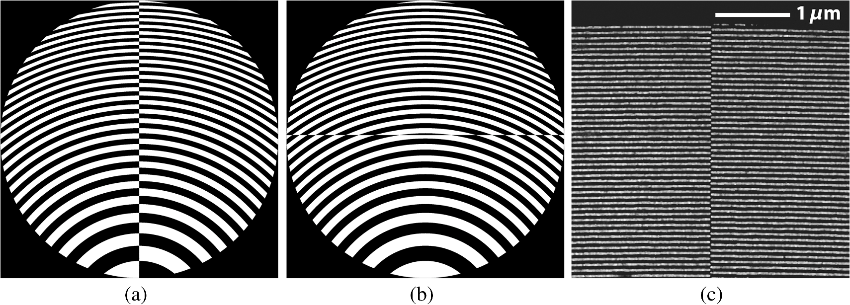 Figures 8(b) and 8(e) show SHARP image data of 175-nm contacts imaged using - and -directional DIC-zoneplates. The size of the contacts is close to the resolution limit of the zoneplates. Thus, the image of a contact closely resembles the point spread function. Figures 8(a) and 8(d) show the phase of the simulated complex electric field in the image plane, multiplied by the amplitude, for a point-like object. A conventional image of 175-nm contacts and the phase of the corresponding simulated electric field are shown in Figs. 9(a) and 9(b) as a reference. The point spread functions of the DIC-zoneplates have two maxima, and in the center, the intensity is zero. The two maxima differ in phase by , as can be seen in Fig. 8(a). The point spread function resembles the discrete derivative operator : the -derivative is applied to the image. In the center of the images, the power is balanced in the two maxima. Outer parts of the object field display some imbalance in power. The amplitude of a wave emerging from an ideal point source is constant in power. The 175-nm contacts are expanded objects that project a diffraction pattern into the pupil. For plane-wave illumination, the distribution of power within the pupil depends on the location of the contact within the object field. For contacts in the centerline of the object field, perpendicular to the direction of the DIC, the power is distributed evenly between the two different sides of the pupil. With increasing distance to the centerline, the imbalance in power across the two sides of the pupil causes an increasing bright-field contribution added to the DIC image. Fig. 8(a) and (d) Magnified simulated false color images, showing the phase of the complex electric field in the sensor plane, multiplied by the amplitude, for a point-like object, imaged with - and -directional DIC-zoneplates. (b) and (e) SHARP image data showing 175-nm contacts, imaged in - and -directional differential interference contrast (DIC). (c) and (f) Image details of 400-nm half-pitch elbows, imaged in - and -directional DIC under coherent illumination. 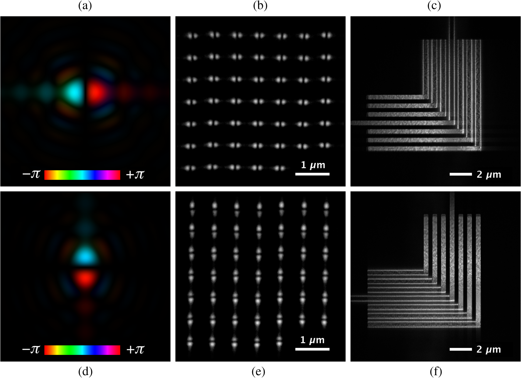 Fig. 9(a) Magnified simulated false color image, showing the phase of the complex electric field in the sensor plane, multiplied by the amplitude, generated by a point-like object, for a standard zoneplate. (b) SHARP image data showing 175-nm contacts, imaged using a standard zoneplate. (c) Image details of 400-nm half-pitch elbows, imaged with a standard zoneplate under coherent illumination. 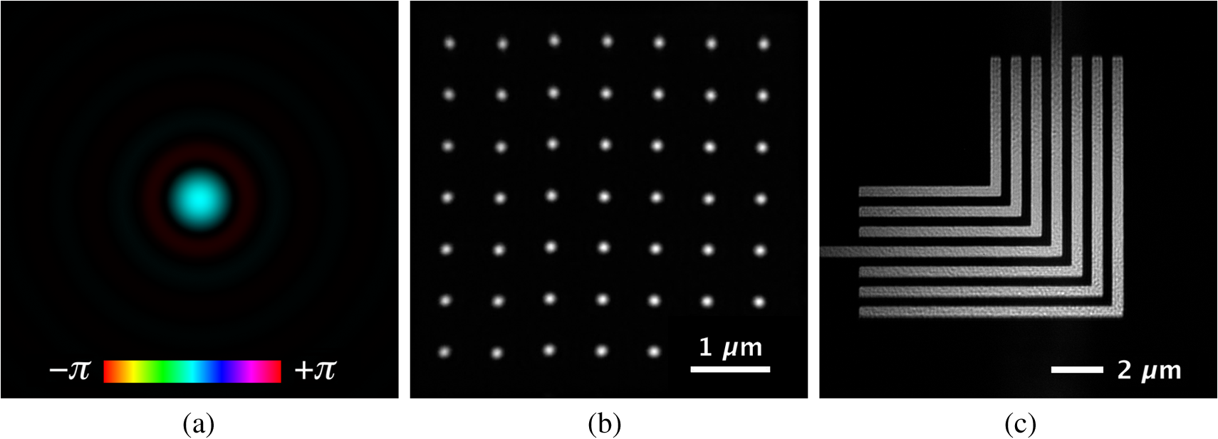 Figures 8(c) and 8(f) show DIC image details of 400-nm elbows. A conventional bright-field image is shown in Fig. 9(c) as a reference. All images of the elbows were recorded with a pupil fill of . Figure 8(c) shows -directional DIC imaging. The central vertical line of the elbow pattern shows clear, -derivative characteristics. The signal is high at the edges and drops to a low value inside the clear line. With increasing distance from the center axis, in addition to signal at the edges of the lines, there is bright-field contribution visible in the clear lines. The granularity is minimized close to the center axis and enhanced in both vertical and horizontal lines away from the center axis. The -directional DIC image shows similar properties. 4.2.Isotropic Differential Interference ContrastThe radial Hilbert transform constitutes another differential contrast enhancing technique. It provides an isotropic measurement of the amplitude and phase gradient in a sample.15 The technique has been implemented, adding a vortex-like phase plate of the form to the back focal plane of an imaging system.16 The phase plate retards the phase by –times along its circumference. Combination of phase modification and focusing power in a single optical element is demonstrated in Ref. 15 for the soft x-ray spectral range. The latter concept is implemented in SHARP, using spiral zone plates of the orders and in an off-axis configuration. Figure 10(a) illustrates the pattern of an on-axis spiral zoneplate of the order . The pattern of an off-axis spiral zoneplate of the order is illustrated in Figure 10(b). Figure 11(b) shows SHARP image details of 175-nm contacts, imaged using a spiral zoneplate. The point spread function is ring shaped. The calculated change in phase along the circumference of the point spread function can be seen in Fig. 11(a). Figure 11(c) shows an image of 400-nm elbows, recorded with the spiral zoneplate. It shows relief-like contrast and edge enhancement in the sweet spot of the lens. The granularity caused by substrate roughness is enhanced compared to the bright-field image. Fig. 10(a) Cartoon of an on-axis spiral zoneplate of the order . (b) Cartoon of a spiral zoneplate of the order in off-axis configuration. 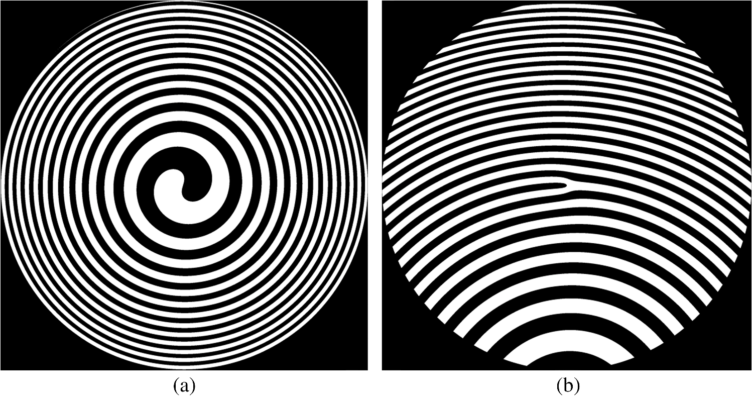 Fig. 11(a) Magnified simulated false color image, showing the phase of the complex electric field in the sensor plane, multiplied by the amplitude, generated by a point-like object, for a spiral zoneplate of the order . (b) SHARP image data showing 175-nm contacts, imaged using a spiral zoneplate. (c) SHARP image details of 400-nm half-pitch elbows, imaged with the spiral zoneplate under coherent illumination. 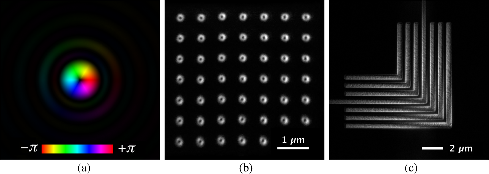 5.Summary and OutlookWe have demonstrated the addition of complementary imaging modes to the SHARP EUV mask microscope in an effort to extract additional information from actinic photomask imaging, to improve navigation, and to enhance defect detection. Zernike phase contrast has been implemented in an actinic EUV mask-imaging tool for the first time and is available to users of SHARP. Early results show significantly enhanced signals from phase defects. DIC in the and directions and isotropic DIC have been demonstrated. The latter techniques increase contrast on a variety of features, including phase defects and intensity speckle from substrate and multilayer roughness. Further activity will be directed at demonstrating the effectiveness of Zernike phase contrast and DIC in real-world defect detection and classification. Cubic phase modulation, dark-field imaging, and stereoscopic imaging are further imaging modes that have been added to the tool, and these will be discussed in further publications. A second chip with zoneplates for additional complementary imaging modes is currently in production. AcknowledgmentsThe Advanced Light Source at Lawrence Berkeley National Laboratory is supported by the Director, Office of Science, Office of Basic Energy Sciences, of the U.S. Department of Energy under Contract No. DE-AC02-05CH11231. We gratefully acknowledge SEMATECH funding of the SHARP microscope, and Anne Rudack the SHARP project manager. Test masks used in imaging experiments described above were provided by GLOBALFOUNDRIES and Intel. ReferencesR. Peeters et al.,
“EUV lithography: NXE platform performance overview,”
Proc. SPIE, 9048 90481J
(2014). http://dx.doi.org/10.1117/12.2046909 PSISDG 0277-786X Google Scholar
C. Wagner et al.,
“EUV into production with ASML’s NXE platform,”
Proc. SPIE, 7636 76361H
(2010). http://dx.doi.org/10.1117/12.845700 PSISDG 0277-786X Google Scholar
P. P. Naulleau et al.,
“Fourier-synthesis custom-coherence illuminator for extreme ultraviolet microfield lithography,”
Appl. Opt., 42
(5), 820
–826
(2003). http://dx.doi.org/10.1364/AO.42.000820 APOPAI 0003-6935 Google Scholar
K. A. Goldberg et al.,
“Actinic mask imaging: recent results and future directions from the SHARP EUV Microscope,”
Proc. SPIE, 9048 90480Y
(2014). http://dx.doi.org/10.1117/12.2048364 PSISDG 0277-786X Google Scholar
K. A. Goldberg et al.,
“Commissioning an EUV mask microscope for lithography generations reaching 8 nm,”
Proc. SPIE, 8679 867919
(2013). http://dx.doi.org/10.1117/12.2011688 PSISDG 0277-786X Google Scholar
R. H. Miyakawa, C. N. Anderson and P. P. Naulleau,
“Zone plate education, design, tolerancing, fabrication, and applications,”
(2014) http://zoneplate.lbl.gov September ). 2014). Google Scholar
F. Zernike,
“Phase contrast, a new method for the microscopic observation of transparent objects,”
Physica, 9
(7), 686
–698
(1942). http://dx.doi.org/10.1016/S0031-8914(42)80035-X Google Scholar
K. P. Nguyen et al.,
“Effect of absorber topography and multilayer coating defects on reflective masks for soft x-ray/EUV projection lithography,”
Proc. SPIE, 1924 418
–434
(1993). http://dx.doi.org/10.1117/12.146524 PSISDG 0277-786X Google Scholar
Y. G. Wang et al.,
“Zernike phase contrast microscope for EUV mask inspection,”
Proc. SPIE, 9048 904810
(2014). http://dx.doi.org/10.1117/12.2048180 PSISDG 0277-786X Google Scholar
G. Schmahl et al.,
“Phase contrast studies of biological specimens with the x-ray microscope at BESSY,”
Rev. Sci. Instrum., 66 1282
(1995). http://dx.doi.org/10.1063/1.1145955 RSINAK 0034-6748 Google Scholar
A. Sakdinawat and Y. Liu,
“Phase contrast soft x-ray microscopy using Zernike zone plates,”
Opt. Express, 16
(3), 1559
–1564
(2008). http://dx.doi.org/10.1364/OE.16.001559 OPEXFF 1094-4087 Google Scholar
G. Nomarski,
“Microinterferometrie differential a ondes polarisés,”
J. Phys. Radium, 16 9
–135
(1955). JPRAAJ 0368-3842 Google Scholar
B. Kaulich et al.,
“Differential interference contrast x-ray microscopy with twin zone plates,”
J. Opt. Soc. Am. A, 19
(4), 797
–806
(2002). http://dx.doi.org/10.1364/JOSAA.19.000797 JOAOD6 0740-3232 Google Scholar
C. Chang et al.,
“Single-element objective lens for soft x-ray differential interference contrast microscopy,”
Opt. Lett., 31
(10), 1564
–1566
(2006). http://dx.doi.org/10.1364/OL.31.001564 OPLEDP 0146-9592 Google Scholar
A. Sakdinawat and L. Yanwei,
“Soft-x-ray microscopy using spiral zone plates,”
Opt. Lett., 32
(18), 2635
–2637
(2007). http://dx.doi.org/10.1364/OL.32.002635 OPLEDP 0146-9592 Google Scholar
J. A. Davis et al.,
“Image processing with the radial Hilbert transform: theory and experiments,”
Opt. Lett., 25
(2), 99
–101
(2000). http://dx.doi.org/10.1364/OL.25.000099 OPLEDP 0146-9592 Google Scholar
BiographyMarkus P. Benk is the project scientist at the SHARP microscope, Center of X-ray Optics, Lawrence Berkeley National Laboratory. He received his diploma in photo engineering from the Cologne University of Applied Sciences in 2006 and his PhD degree from RWTH Aachen University in 2011. He has authored and co-authored several papers on extreme ultraviolet and soft x-ray imaging. His current research interests include sources, metrology and optics for soft x-rays, and extreme ultraviolet light. Ryan H. Miyakawa is an EUV project scientist at the Center for X-ray Optics at Lawrence Berkeley National Lab, where he works with the SEMATECH Berkeley MET performing EUV imaging, interferometry, and lithography. Weilun Chao leads the nanofabrication group of the Center for X-ray Optics. He received his PhD in electrical engineering from University of California, Berkeley, in 2005. He specializes in electron-beam-based lithographic processes for dense nanostructures and EUV/x-ray diffractive optics. Current research interests include complex diffractive optics, 3-D nanostructures, and nanodevices for life science. Yow-Gwo Wang received his BS degree from the Department of Electrophysics and the MS degree from the Institute of Electro-Optical Engineering at National Chiao Tung University in 2009 and 2011, respectively. Currently he is a PhD student at the University of California at Berkeley and also a graduate student researcher at Lawrence Berkeley National Laboratory. His research is focusing on design, fabrication, and testing of mask/lens concept for EUV aerial image monitoring and inspection. Antoine Wojdyla is a postdoctoral fellow at the Lawrence Berkeley National Laboratory's Center for X-Ray Optics. He received his PhD degree from École Polytechnique in 2011, where he studied time-domain phase imaging in the far infrared range. His research interests include optical instrumentation and computational analysis of image data. David G. Johnson is a research associate at the Lawrence Berkeley National Laboratory's Center for X-Ray Optics, specializing in extreme ultraviolet mask imaging and technologies for short-wavelength applications. He has developed methods for electron-beam fabrication of holographic lenses and previously conducted experiments in air quality monitoring. He holds dual BS degrees in physics and in civil and environmental engineering of the University of California, Davis. Alexander P. Donoghue is a research associate at the Lawrence Berkeley National Laboratory's Center for X-Ray Optics, working in EUV mask inspection and development of experimental systems for short-wavelength applications. He previously worked as a controls and data systems engineer for the Linac Coherent Light Source at the SLAC National Accelerator Laboratory. He holds a BS degree in physics from California Polytechnic State University at San Luis Obispo. Kenneth A. Goldberg is the deputy director of the Center for X-Ray Optics at Lawrence Berkeley National Laboratory, specializing in the development of EUV and soft x-ray technologies, including lithography, mask imaging, and wavefront measuring interferometry. He is the principal investigator of the SHARP EUV photomask imaging microscope. He received an AB degree in physics and applied math, and a PhD in physics from the University of California, Berkeley. |


