|
|
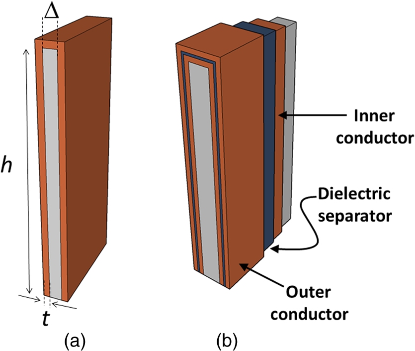
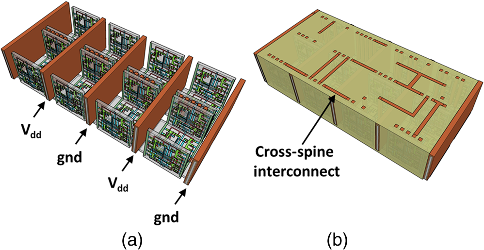
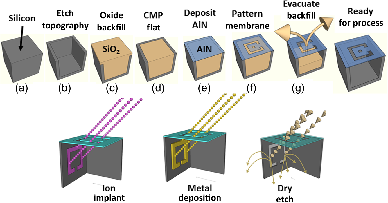
1.IntroductionMoore’s law,1 an observation that the cost per transistor decreases as transistor density increases, following a roughly two year doubling period, has dominated the landscape of semiconductor research since it was first proposed in 1965. For much of this run, Moore’s law was supported by Dennard scaling2 which posits that processing performance per Watt increases with decreasing device dimension, which also possesses a similar doubling period. Thus, the reduced cost per transistor was accompanied by higher performance per Watt, a win–win proposition which served as a self-sustaining feedback mechanism, responsible for today’s massive semiconductor and personal electronics industries among other epochal changes. This coincidental scaling of cost, performance, and power consumption allows these trends to be conveniently plotted on familiar log-linear graphs showing the breathtaking ascent and, more recently, inevitable stall of these curves as the semiconductor industry has eclipsed the 28-nm processing node. Transistors with smaller device dimensions are subject to a variety of deleterious effects such as drain induced barrier lowering, gate leakage, subthreshold leakage, and so on responsible for the end of Dennard scaling. Even though subsequent lithography nodes add higher transistor density, the failure of these new device designs to scale power requirements means that not all of these transistors can be concurrently active for the same power budget, leading to the notion of dark silicon, a problem which scales nonlinearly with shrinking dimensions. In addition to these deterministic effects, small transistors also incur increased variance of the statistical distribution of device performance. Increasing variability in performance from device to device complicates the already enormous task of designing circuits and multicircuit modules.3 Pursuit of Moore’s law has required more than just smaller transistors. Adoption of increasingly complicated interconnection strategies has also been necessary in order to allow the dense sea of transistors to communicate with one another. For some time, it has been recognized that gate delay and transistor capacitance are only a fraction of the overall delay in switching speed.4 Interconnect capacitance has dominated gate delay, forcing the adoption of copper damascene and pursuit of low-k dielectrics. The culmination of this trend is the inclusion of air-gaps to further reduce capacitance by filling the space between interconnects with a material with the lowest possible dielectric constant at the cost of manufacturing complexity, yield, and potential reliability concerns. Modern integrated circuits are highly optimized to maximize performance per unit area. Shrinking device dimensions and areal scaling are achieved through process node improvements, fueling much of this optimization, however, design process technology cooptimization, the practice of using process-aware design of circuit layout has become increasingly important.5 Adoption of Manhattan layout geometry and self-aligned double/quadruple patterning (SADP, SAQP) are examples where full two-dimensional (2-D) interconnect spatial freedom is sacrificed in order to enable advanced lithography techniques. Optimized module designs are constructed with the optimized transistors. In order to connect these modules together, sophisticated place and route algorithms are used to construct larger computational blocks. These increasingly disruptive trends have forced the semiconductor industry to adopt new materials, process techniques, and device design concepts, with even more drastic changes required for future process nodes.6 Adoption of a 3-D integrated circuit topology is seen by many in the industry as a viable approach to continue density scaling. The shorter average interconnect lengths of three-dimensional integrated circuits (3-D-ICs)7 reduce both the resistance and capacitance of the line, and hence reduce ohmic power dissipation and RC time delay. While just on the verge of being adopted as a high volume manufacturing (HVM) solution, the concept and advantages of 3-D-ICs have been identified since at least the 1980s.8 In its current incarnation, 3-D-IC architectures are divided into two distinct types: (1) 3-D-ICs created by stacking planar 2-D chips,9 achieving interconnection in the vertical direction using through silicon vias (TSV); and (2) monolithic 3-D-ICs where epitaxial regrowth is performed on the wafer after fabrication of the first layer of devices, yielding a second layer of single crystal silicon for a second layer of silicon devices.10 Both of these approaches yield ICs with current flow vertical to the wafer surface, and, in that sense are 3-dimensional, however, the transistors forming each integrated circuit all have their active regions oriented parallel to the wafer surface. The purpose of this paper is to point out that another class of 3-D-ICs exists with transistors oriented along each of the coordinate axes. Distinct from both TSV-3-D-ICs and monolithic 3-D-ICs, these take full advantage of the third-dimension at the device and module level to affect increases in trace width and trace separation, reducing interconnect resistance and capacitance, while capturing the inherent reduction in average interconnect length that comes with 3-D interconnection. Each of these helps to improve the interconnect delays and power dissipation which threaten to make further lithography node scaling ineffectual. Furthermore, we advance an oblique processing approach, membrane projection lithography (MPL), as a fabrication method capable of fabricating this new class of 3-D-ICs, requiring only minimal fixturing changes to current state-of-the-art semiconductor fabrication equipment. 2.Advantages of Device-Level Three-Dimensional Integrated CircuitsEven in 2-D topologies, layout, placement, and routing are all enormously complex endeavors. In the discussion that follows, no attempt has been made to generate optimal designs or to consider the myriad codependent constraints that exist in an actual circuit design, but rather to advance 3-D specific design possibilities that cannot be adopted by a 2-D approach, or for that matter, 3-D-ICs in either a TSV or monolithic approach. Consider the planar multimodule layout in Fig. 1(a). This layout block consists of three -by- micrometer sections with many transistors. The areal footprint of this block is . Furthermore, an interconnect is required from points 1 to 2 (noted by the yellow stars in the figure). Given the dimensions of the block, this interconnect will be micrometers in length, and the trace will be stood off from the metal layers beneath it by the height of the underlying metal layer, typically in the deep submicrometer regime. Without addressing how this is to be done for the moment, assume that the two end sections of the block are folded up [Fig. 1(b)] so that they form right angles with the middle section as shown in Fig. 1(c). The device layer of silicon for the two edge sections has a thickness , and the current flow for the transistors in the two edge sections is contained in the -plane rather than the -plane. The block in Fig. 1(c) has an areal footprint of , so that for , the configuration in Fig. 1(c) has nearly a factor of 3 increase in areal transistor density versus the planar case in Fig. 1(a). Fig. 1(a) Planar logic module in size. Interconnect from point 1 to point 2 is micrometers long; (b) folding the two edges of the planar module allows for module level three dimensionality; and (c) same module folded into 90 deg segments. The distance from point 1 to point 2 is only W micrometers long. 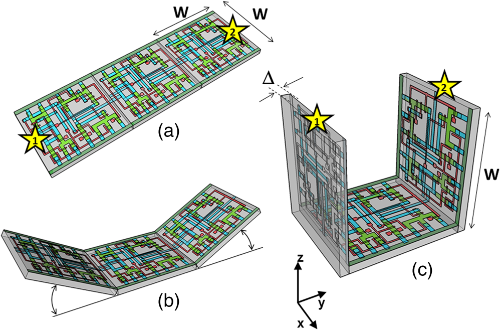 The interconnect from points 1 to 2 is now shortened from to , a factor of 3 reduction, while the separation of the trace connecting these two points with the underlying metal layers becomes , significantly greater than in the planar case. Shortening the interconnect length reduces ohmic loss and distributed capacitance. Furthermore, the increased separation reduces capacitance and cross talk. In a planar geometry, the separation between traces is fixed by the metal thickness. To lower the capacitance between traces in a 2-D geometry, the only knob to tweak when the distance between traces is fixed is to pursue inter-layer dielectrics (ILD) with smaller dielectric constants. A meaningful reduction in dielectric constant over dense ILDs is only achieved by incorporation of porosity, which necessarily impacts process robustness. Given that the relative dielectric constant of air is 1 and is 4, the maximum achievable reduction in capacitance through material changes is 4. In reality, has already been replaced by materials with , so that there is much less room for further improvement through material selection. Exploring the advantages of 3-D topology even further, consider Fig. 2. In Fig. 2(a), two parallel traces with thickness, , are oriented horizontally and stacked vertically. Treating these two traces as a parallel plate capacitor, the capacitance between the two traces is given by where is the cross sectional area of the plates (given by ), is the separation of the plates, and is the dielectric constant of the material separating the traces. In Fig. 2(b), the same traces are oriented vertically and stacked vertically, separated by the same distance, . In this case, the cross sectional area between the two traces is given by , so that for , the capacitance . Since the physical dimensions of the traces in both cases are identical, they both possess equivalent current carrying capacity and resistivity. Furthermore, consider the areal footprint of the traces as measured in the -plane. The traces in Fig. 2(a) have a footprint of whereas the traces in Fig. 2(b) have a footprint of , which, if , has the same current capacity and resistance, smaller capacitance, and a smaller footprint.Fig. 2(a) Two horizontally stacked copper interconnect traces with dimensions , separated by a distance and (b) two vertically stacked copper interconnect traces with dimensions , separated by a distance , with significantly reduced capacitance. 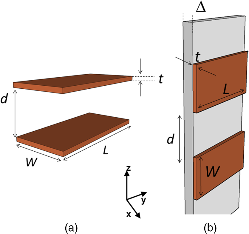 As a further example of the possible leverage a fully 3-D approach has, consider Fig. 3(a), where a trace with a thickness is deposited over a silicon feature with height and width . The resulting trace has a cross sectional area proportional to , while occupying an areal footprint of just (). Another advantage of a “spine” interconnect such as this is in addition to the large cross sectional area is that it serves as a common interconnect for devices on the left and right side of the spine simultaneously. It is also possible to create coaxial or core-shell interconnects like those shown in Fig. 3(b), where significant shielding is gained. While modern interconnects bear little resemblance to the parallel plate traces of Fig. 2(a), the principles and potential advantages remain. 3.Device Level Three-Dimensional Integrated Circuit GeometryFrom Sec. 2, we saw that the folded, 3-D version of the logic block has a increase in areal transistor density, which is attractive. However, aside from the complete lack of manufacturability of such a folding scheme, this approach has at least one more fatal flaw: neighboring modules cannot be densely packed together so that the chip level density remains the same. This can be remedied in a highly manufacturable way, however, as 3-D-ICs can be created in a dense array of 3-D modules by fabricating the transistors in high aspect ratio (HAR) machined silicon. Figure 4(a) shows two back-to-back 3-D modules in just one of several possible HAR 3-D motifs. In this case, each module has a device silicon thickness of , while adjacent modules are separated by a gap of distance . The length, , of the modules is a free parameter, while the height, , is constrained by the resultant aspect ratio (AR) of either the vertical device layer or the gap, depending on their dimensions. Etched ARs of are fairly routine. In principle, long modules with can be fabricated, however, it might be advantageous to include orthogonally positioned spines with a separation , from the vertical device module fin as shown in Fig. 4(b). Fig. 4(a) One possible etched, HAR silicon matrix for a “nonfolded” fabrication approach to device level 3-D-ICs and (b) HAR silicon matrix including orthogonal interconnect spines. 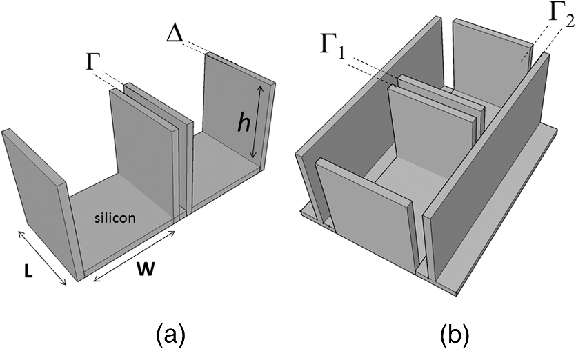 Combining the HAR structure with 3-D interconnect motifs allows construction of larger functional blocks. Figure 5(a) shows a single module with large surface area, spine interconnects. Whereas global signals such as the power rails and clock signals are typically distributed at the highest metal level and then multiplexed down to the individual transistors, in this instance, these spines can be used to route global signals down at the silicon level (L0 metal?). Inclusion of “hitching post” vias in the gap allows for short interconnection between adjacent 3-D modules, further reducing average interconnect length [Fig. 5(b)]. These vias can be formed in the same step as the power rail formation as long as suitable isolation is introduced. By etching through the device and isolation layers on both sides of the via, interconnection between the two faces is achieved. Fig. 5(a) 3-D logic block combined with spine interconnects for global distribution of power and (b) examples of “hitching post” vias to allow for intermodule interconnects and vertical signal routing. 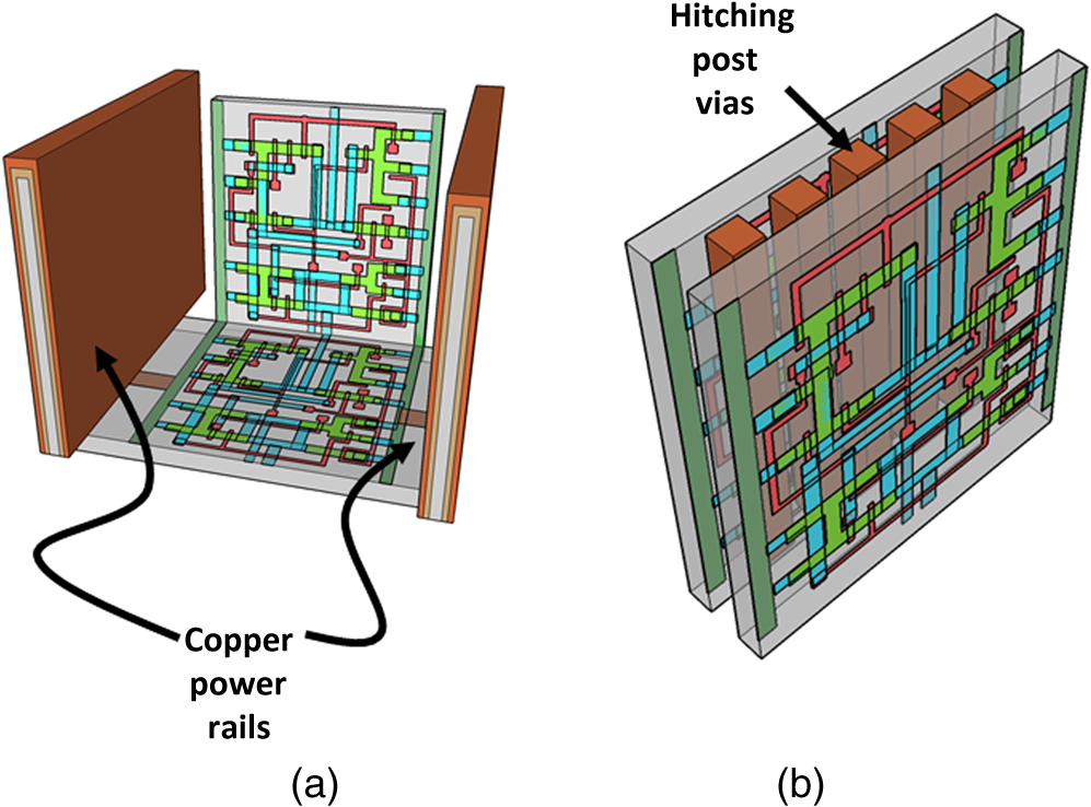 Figure 6 contains the vision of larger chip level constructs built up from many multimodules. In Fig. 6(a), neighboring multimodule blocks are separated by spine interconnections with global interconnects. The double-sided spines allow the global signals to be interleaved. Figure 6(b) shows the same blocks backfilled and planarized via chemically mechanically polished (CMP). At this point, standard back end of line (BEOL) processing can be used to build up intermediate length interconnects and higher layer global interconnects. 4.Membrane Projection LithographyWith the geometry and some interconnect strategies established, the only remaining question is “How do we create transistors on the vertical faces of silicon?” Fabrication of CMOS devices requires “blanket” process steps such as oxidations and chemical vapor deposition (CVD)/atomic layer deposition (ALD) depositions, as well as patterned, directional steps such as ion implantation, dry etching, and metal deposition. Since most blanket steps such as oxidation and CVD/ALD deposition can be performed conformally, demonstration of oblique versions of ion implantation, dry etching, and metal deposition enables fabrication of MOSFETs in high-aspect ratio silicon topography. The key to achieving oblique processing is MPL, a technique which creates suspended inorganic membranes patterned with the desired pattern over 3-D topography etched in single crystal silicon using standard CMOS equipment.11–13 Figure 7 shows a schematic sequence of the MPL process. Starting from planar silicon 7(a), the desired topography is etched 7(b), backfilled with CVD oxide 7(c), and CMP flat. An aluminum nitride (AlN) film is deposited 7(e), patterned using standard lithography, and etched 7(f). The backfill oxide is then evacuated using hydrofluoric acid 7(g). At this point, the AlN film exists as a patterned membrane suspended over the HAR silicon, serving as a stencil for patterning the underlying silicon through ion implantation, metal deposition, or dry etching. After processing, the membrane is removed using a version of the standard SC1 clean (, at 70°C). The MPL approach is quite general, however, it does require that the membrane patterns be self-supporting; closed loops in the pattern cannot be transferred as the center of the loop will not be supported and will fall through the membrane. Figure 8 contains proof-of-concept demonstrations of the three directional steps of ion-implantation, metal deposition, and dry etching. Figure 8(a) contains the results of a process simulation (Athena) showing patterned implant through a 1000 Å thick silicon nitride membrane. While the composition and thickness of the membrane and implant dose have not been optimized, the ability of a thin membrane to successfully define a high-dose implant region on the vertical sidewall is established. In Figs. 8(b) and 8(c), SEM images of deposited metallic 8(b) and etched features 8(c) are shown. The structures were all fabricated on 150-mm wafers, using 248-nm optical lithography. Although the HAR silicon patterning in these SEMs is suboptimal, it is apparent that high fidelity patterns can be produced using this method. Fig. 8(a) Athena process simulation demonstrating that a 1000 Å thick nitride membrane is capable of defining a patterned region on the vertical sidewall; (b) tilted, cross-section SEM image of vertically oriented metal depositions on the silicon sidewall and (c) tilted cross-section SEM image of etched features on a vertically oriented silicon sidewall. Scale Bars in (b) and (c) are . 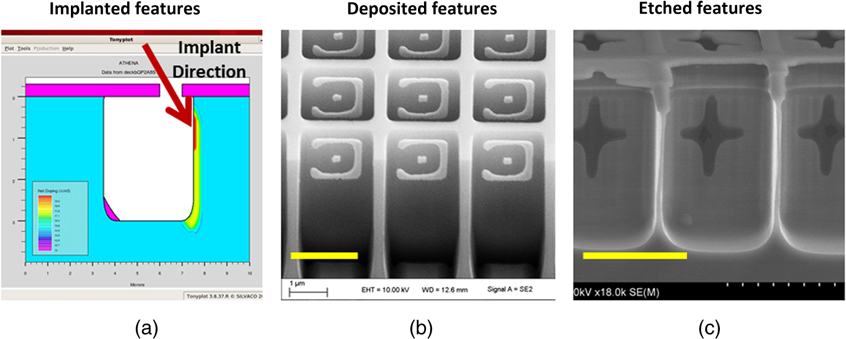 Both ion implantation and metal deposition (sputtering and e-beam evaporation) are highly directional processes so that positioning the substrate at an angle with respect to the incoming flux results in either implantation or deposition through the membrane onto the vertical sidewall. For metal deposition, a Temescal e-beam evaporation system was used with a chamber pressure of to . The neutral metal flux forms a high fidelity line-of-sight replica of the membrane pattern on the sidewall. Dry etching is different than either implantation or metallization due to the formation of a plasma used to create and accelerate the etchant species toward the etch platen. During etching, a plasma sheath conforms to the substrate, accelerating the ions normal to the substrate. Using a Faraday cage, the direction of the ion acceleration can be altered so that oblique etching will occur.14–17 We have demonstrated patterned oblique etching using both reactive ion etch and inductively coupled plasma etch systems using a Faraday cage to direct the etchant species obliquely. Our Faraday cage was machined into a wedge out of a solid stainless steel block. Stainless steel mesh with a wire diameter of and grid spacing of formed the ion-permeable membrane. The MPL approach is presented here with an backfill and AlN membrane, but the choice of materials is quite broad. The only requirement is that the backfill, membrane, and silicon topography (possibly lined with barrier materials) form an orthogonal processing set, where the membrane and backfill materials can be deposited and removed without impacting the other components. We have used base-developable polyimide and polysilicon (with a nitride lined topography) in addition to as the backfill material and photoresist, and poly methyl methacrylate, tungsten and germanium in addition to the AlN, for the membrane material. While we have yet to experience any issues in completely removing the backfill material from high aspect ratio topography using an aqueous dissolution of the , vapor- and plasma-based dissolution are also an option. For instance, we have used a chemical downstream etch with to remove polysilicon backfill, and vapor phase HF can be used to remove . 5.Prospects for Integration to High Volume Manufacturing FabricationThe MPL process demonstrated uses CMOS compatible materials and standard semiconductor processes and equipment. Lithographic patterning of the membrane occurs on a CMP-flat surface, compatible with any type of lithography including state of the art high NA immersion steppers. Oblique ion implantation is currently used for halo implants and is already in HVM. For metal deposition, the only change required is a fixture for positioning the wafer at an angle to the source as well as methods for homogenizing the metal flux, as the wafers cannot be rotated during deposition. Additionally, the metal process is inherently a “lift-off” process, which has been replaced in the industry by either blanket deposit/etch or damascene patterning. BEOL processing of interconnects can still be performed using standard copper damascene. The introduction of a Faraday cage into the etch chamber necessary for patterning sidewalls can be handled seamlessly by creating a wafer clamp ring with individual die-level Faraday cages (Fig. 9). Again, this only involves a minor fixturing change, which adapts current capital equipment into a tool-set capable of oblique processing. Fig. 9Etch chamber clamp ring with die-level Faraday cages oriented at a 45-deg angle with respect to the wafer surface for etching vertical sidewalls. 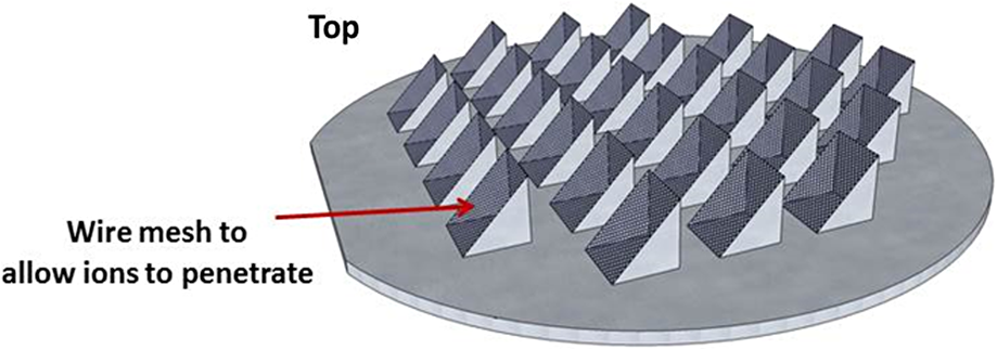 Patterning using the MPL approach requires that steps (c)–(g) in Fig. 7 are repeated each time a new pattern must be transferred. Fortunately, the industry has already embraced multiple patterning steps in order to enable the SADP/SAQP approach, so this is perhaps not as onerous a requirement as it might seem, and is only necessary for front end processing. Furthermore, it is possible that device layouts could be constructed which reuse the same membrane pattern for each of the device faces by exploiting device module symmetry. We have yet to rigorously establish the resolution limits of MPL, but we have anecdotal evidence that isolated features are resolvable. Dense line/space patterns may be more problematic. Clearly, thinner membranes allow for finer features at the expense of structural integrity for the membrane. Another concern is the need for wafer alignment in the tool. Whereas alignment and overlay of the optical lithography to pattern the membrane remain unchanged from a planar process, the projection of that pattern by the etch, deposition, or implant operation is based on the trajectory set by both the in-plane and out of plane rotation of the wafer with respect to the source, and must be controlled to a tight tolerance. While fabrication in the “folded” space of the HAR silicon matrix increases areal transistor density by nearly a factor of 3, the need for gaps, and device silicon thickness as well as (optional) interconnect spines cut into this gain. Additionally, the prospects of creating a finFET transistor on the sidewalls are remote, so transistor designs from earlier than the 45-nm node are probably required. Finally, adopting this 3-D-IC fabrication approach does not preclude the use of TSVs for chip/wafer stacking or monolithic regrowth for subsequent layers of 3-D transistors, should either approach be adopted by industry. The hope is that the reduction in interconnect resistance and capacitance won by adopting this 3-D approach yields net advantages over higher density planar designs fabricated using the standard approach in a planar topology. While the story arc of Moore’s law would tend to disagree with this, some cracks are beginning to form in the prevailing narrative, “from at least the 45-nm node, we can create smaller logic blocks using gate pitches larger than nominal, owing to the combined effects of parasitics, strain, and lithography limitations.”3 6.ConclusionsThe challenges outlined in Sec. 5 are substantial. For almost the entire history of the IC industry, such a reimagining of the fabrication of transistors at the device level would have been summarily dismissed. But these are interesting times. Industry conferences are full of sessions considering materials to replace silicon (carbon nanotubes, graphene, , and so on), steeper subthreshold devices (tunnelFETs), phase change materials (MEMristors), and nonvon Neuman computing solutions (the last three of which usually also require nonsilicon starting material). Such massive departures from silicon based, charge control, CMOS fabricated with optical lithography represent a long horizon endeavor, with many years (decades?) of research. In that light, the fact that we can generate such a specific, if incomplete, list of challenges to 3-D-ICs fabricated with MPL could be seen as an endorsement—the present approach leverages 60+ years of research into -type and -type contacts to silicon, gate stack engineering, drain, and source engineering, 450-mm starting material, CMP, design, layout and placement, and routing. We are able to judge the MPL approach so critically because it exists in a space we are familiar with; we have the callouses and scar tissue as evidence. Some of these tried and true notions may have to be discarded or adapted, but at least the issues are known. Adopting a nonsilicon based approach abandons much of this hard-won insight, and makes it difficult to assess the first order issues with a new technology, let alone the show-stopping, devil’s in the details issues which are more than enough to engulf and quash a seemingly promising direction. The seriousness with which these alternatives are being considered speaks to the enormity of the task to extend Moore’s law scaling of computing performance, if not transistor density. An alternative to continuing to simultaneously address cost, performance, and power is to split the application space into segments which are highly sensitive to improvements in one axis, while being tolerant of suboptimality in the other two. Perhaps ever-increasing density through device scaling was a guide star followed one or two process nodes too far for some of these applications. In contemplating such a fractured application space, it is possible that the 3-D-IC approach advanced here could provide an acceptable balance between process complexity and device performance in applications where the density of a few lithography nodes ago combined with reduced interconnect capacitance and resistance yield a superior product. AcknowledgmentsSupported by the Laboratory Directed Research and Development program at Sandia National Laboratories, a multiprogram laboratory managed and operated by Sandia Corporation, a wholly owned subsidiary of Lockheed Martin Corporation, for the U.S. Department of Energy’s National Nuclear Security Administration under contract DE-AC04-94AL85000. ReferencesG. Moore,
“Cramming more components onto integrated circuits,”
Electron. Mag., 38 114
–117
(1965). http://dx.doi.org/10.1109/JPROC.1998.658762 NMAACRESMICK 1476-11220305-9766 Google Scholar
R. H. Dennard et al.,
“Design of ion-implanted MOSFET’s with very small physical dimensions,”
Proc. IEEE, 87 668
–678
(1999). http://dx.doi.org/10.1109/JPROC.1999.752522 IEEPAD 0018-9219 Google Scholar
G. Yeric,
“Moore’s law at 50: are we planning for retirement?,”
in IEEE Int. Electron Devices Meeting (IEDM 2015),
1.1.1
–1.1.8
(2015). http://dx.doi.org/10.1109/IEDM.2015.7409607 Google Scholar
K. Buchanan,
“The evolution of interconnect technology for silicon integrated circuitry,”
in GaAs MANTECH Conf.,
(2002). Google Scholar
L. Liebmann et al.,
“Simplify to survive, prescriptive layouts ensure profitable scaling to 32 nm and beyond,”
Proc. SPIE, 7275 72750A
(2009). http://dx.doi.org/10.1117/12.814701 PSISDG 0277-786X Google Scholar
International Technology Roadmap for Semiconductors 2012-Design,
(2012). Google Scholar
D. Stroobandt,
“Recent advances in system-level interconnect prediction,”
IEEE Circuit Syst. Newsl., 11
(4), 4
–20
(2000). Google Scholar
Y. Akasaka,
“Three-dimensional IC trends,”
Proc. IEEE, 74 1703
–1714
(1986). http://dx.doi.org/10.1109/PROC.1986.13686 IEEPAD 0018-9219 Google Scholar
A. W. Topol et al.,
“Three-dimensional integrated Circuits,”
IBM J. Res. Dev., 50 491
–506
(2006). http://dx.doi.org/10.1147/rd.504.0491 IBMJAE 0018-8646 Google Scholar
S. Wong et al.,
“Monolithic 3D integrated circuits,”
in Proc. of Technical Papers, Int. Symp. on VLSI Technology, Systems and Applications,
(2007). http://dx.doi.org/10.1007/978-0-387-76534-1_2 Google Scholar
D. B. Burckel et al.,
“Fabrication of 3D metamaterial resonators using self-aligned membrane projection lithography,”
Adv. Mater., 22 3171
–3175
(2010). http://dx.doi.org/10.1002/adma.200904153 ADVMEW 0935-9648 Google Scholar
D. B. Burckel et al.,
“Micrometer-scale cubic unit cell 3D metamaterial layers,”
Adv. Mater., 22 5053
–5057
(2010). http://dx.doi.org/10.1002/adma.v22.44 ADVMEW 0935-9648 Google Scholar
D. B. Burckel et al.,
“Micrometer-scale fabrication of complex three-dimensional lattice+basis structures in silicon,”
Opt. Mater. Exp., 5 2231
–2239
(2015). http://dx.doi.org/10.1364/OME.5.002231 Google Scholar
G. D. Boyd, L. A. Coldren and F. G. Storz,
“Directional reactive ion etching at oblique angles,”
Appl. Phys. Lett., 36 583
–585
(1980). http://dx.doi.org/10.1063/1.91554 APPLAB 0003-6951 Google Scholar
J.-K. Lee et al.,
“Oblique-directional plasma etching of Si using a Faraday cage,”
J. Electrochem. Soc., 156 D222
–D225
(2009). http://dx.doi.org/10.1149/1.3122623 JESOAN 0013-4651 Google Scholar
S. Takahashi et al.,
“Direct creation of three-dimensional photonic crystals by a top-down approach,”
Nat. Mater., 8 721
–725
(2009). http://dx.doi.org/10.1038/nmat2507 Google Scholar
D. B. Burckel et al.,
“Oblique patterned etchning of vertical silicon sidewalls,”
Appl. Phys. Lett., 108 142103
(2016). http://dx.doi.org/10.1063/1.4945681 Google Scholar
BiographyD. Bruce Burckel received his PhD from the University of New Mexico in Engineering in 2004. He joined Sandia National Laboratories as a postdoc (2005) and then staff member (2008), where he is currently a principal member of the technical staff. Along with inventing the membrane projection lithography technique, he researches a variety of nano- and microscale 3-D fabrication techniques. |