|
|
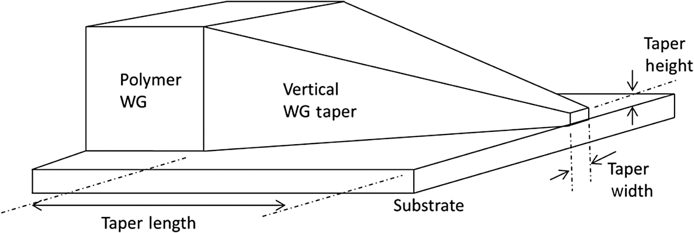
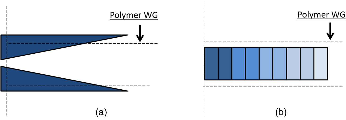
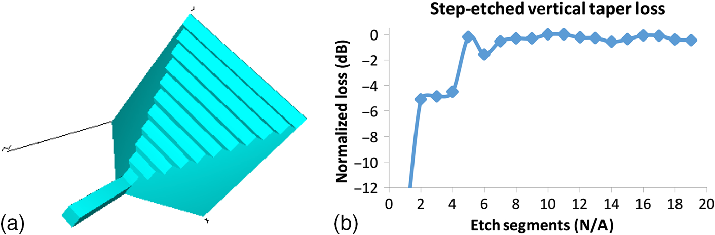
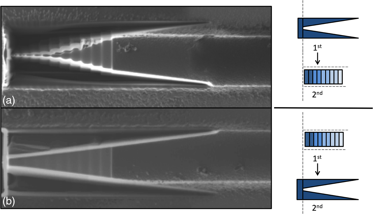
1.IntroductionDirect-light coupling into and out of integrated silicon (Si) photonic devices can be performed using low-attenuation ()1 silica-based single-mode fibers (SMFs). Direct coupling between Si waveguides (WGs; , ) and SMFs (, ) results in high coupling loss ().2 Photonic-bridge modules minimize optical coupling loss, allow for system flexibility in device connectorization, and eliminate expenses required for conducting end-face treatments on both Si WGs and SMFs.3 A photonic-bridge module utilizing a WG taper design shown in Fig. 1 is manufactured using low-loss polymer materials on a metallic-coated substrate. The taper acts as a mode expander that gradually transforms the propagating fundamental mode to improve modal overlap between the interfacing WGs. A metal undercladding maintains the high NA necessary for efficient coupling with Si WGs by ensuring modal confinement during adiabatic mode transformation. Though the metallic cladding layer induces significant absorption loss as a function of distance, a minimum length is required for the taper to convert between modes adiabatically and eliminate substrate radiation.3 Polymer WG materials exhibit low absorption loss and can be molded through a variety of cost-effective manufacturing techniques, including soft-imprint lithography.4 Initial taper prototypes fabricated using photolithography demonstrated high loss due to optical scattering from sidewall roughness of [ RMS (root-mean-squared)]. To alleviate sidewall roughness focused ion beam (FIB), techniques are investigated to manufacture the taper portion in a single-processing step. The FIB has many unique applications, including transmission electron microscopy sample preparation, micromachining, and selective metal deposition. Due to the pixel-based raster scanning process of the FIB etching out large devices is slow (). 2.Optical Waveguide Taper Manufacturing LayoutPrototyping low-loss tapers with high resolution was performed utilizing the FIB to mill out tapers at the end of premanufactured polymer WGs. Polymer WGs were fabricated with traditional photolithography on a gold-coated substrate and cleaved to acquire smooth polymer WG end-faces. As shown in Fig. 2, WG ends are milled into taper structures with appropriate dimensions () for both adiabatic mode conversion and efficient Si WG coupling. The etching process includes multiple steps to shape the WG end-face horizontally and vertically for three-dimensional mode conversion, which can be seen in Fig. 3. Furthermore, most FIB platforms are not equipped with the ability to mill out continuous vertical tapers over a specified scan length. Alternatively, vertical tapers can be etched out with a minimum number of discrete steps with minimal loss in mode conversion, as shown in Fig. 4. Simulated results illustrate that the minimum number of etch steps for adiabatic mode conversion is etch segments. Fig. 2The ends of polymer WG straights (photolithography) will have their end-faces etched out (FIB) into tapers. 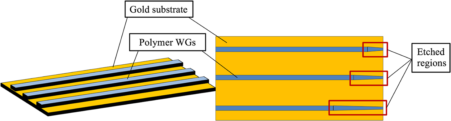 3.Optical Waveguide Taper Fabrication3.1.Focused Ion Beam CalibrationSince the FIB platform is not equipped with an e-beam imaging system, scattered electrons from the rastered ion beam are collected and measured for imaging and sample alignment. The ion beam is controlled externally by utilizing the Nanometer Pattern Generation System (NPGS). Imported DesignCAD files are written on a pixel-by-pixel basis to create the desired image. NPGS can control the amount of pixel overlap, as shown in Fig. 5, to minimize regional ionization (low overlap) and image resolution (high overlap). With the FIB spot size measured at 100 nm in diameter, the optimal pixel spacing was observed at . Fig. 5(a) Illustration demonstrating pixel dose with varying degrees of overlap; (b) step etching demonstrating sufficient versus insufficient pixel spacing for polygon etching.  The raster scanning procedure to complete the milled object can be split into multiple passes to incrementally etch out the desired pattern without overcharging the dielectric material. Increasing the number of etch passes () has been shown to increase etch anisotropy and decrease etch roughness.5 Furthermore, incremental passes significantly reduce the level of material redeposition. Experimental results demonstrated that smooth etching is observed when at least 10 passes are utilized per of etch depth. To acquire a quantitative etch rate polymer, WG end-faces were step-etched at known dose rates. The etch depth was measured and compared to the known WG height to acquire the etch depth at the specified etch dose. The data plotted in Fig. 6 show an etch rate of . A nonzero -intercept is observed as a result of the unavoidable etching properties of the rastered ion beam during imaging and alignment to the polymer WG. 3.2.Taper FabricationFIB milling of rectangular polymer WGs above a flat substrate resulted in unforeseen issues when the beam interacted simultaneously with the polymer WG and the substrate. As shown in Fig. 7, an ion beam induces vertical etching directly from the beam and horizontal etching from ejected ions from the substrate resulting in increased etch rates producing high sidewall roughness and uneven horizontal surfaces. Smooth etching of stepped vertical tapering is achieved by containing the milling beam within the polymer WG, as shown in Fig. 8. Fig. 7(a) Illustration and (b) SEM images of a polymer WG end-face processed with a step-etch polygon etch; unwanted horizontal etching is observed from beam interactions with the substrate. 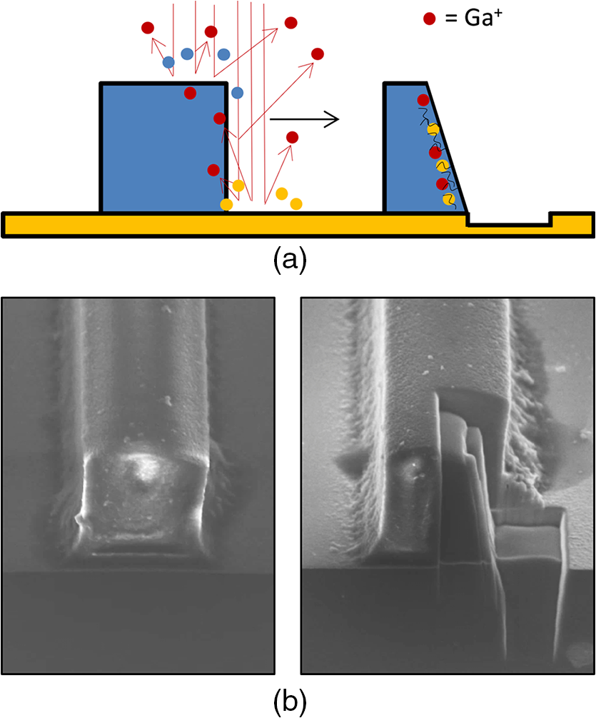 Polymer WG tapers require both horizontal and vertical etching steps both requiring their own etching parameters described in Table 1. Ion beam interaction is important in milling out the desired structure requiring vertical tapering to be conducted before horizontal tapering and completely within the polymer WG. The importance of maintaining etch order to acquire the final device structure is shown in Fig. 9. The procedure was extended to fabricate polymer WG tapers with the lengths of 10 and for FIB testing and functional prototypes respectively, as shown in Figs. 10 and 11. Table 1Etching properties utilized in mill out the horizontal and vertical steps in polymer taper fabrication.
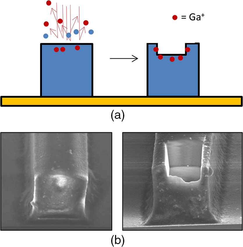
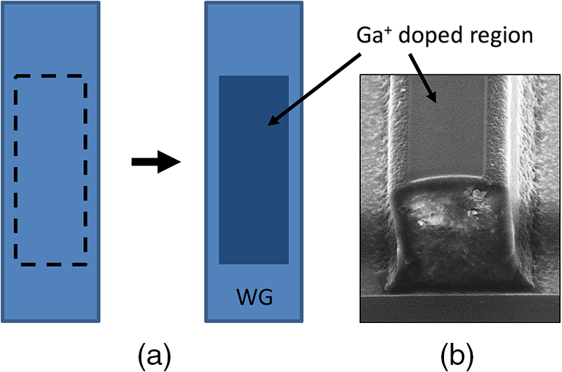
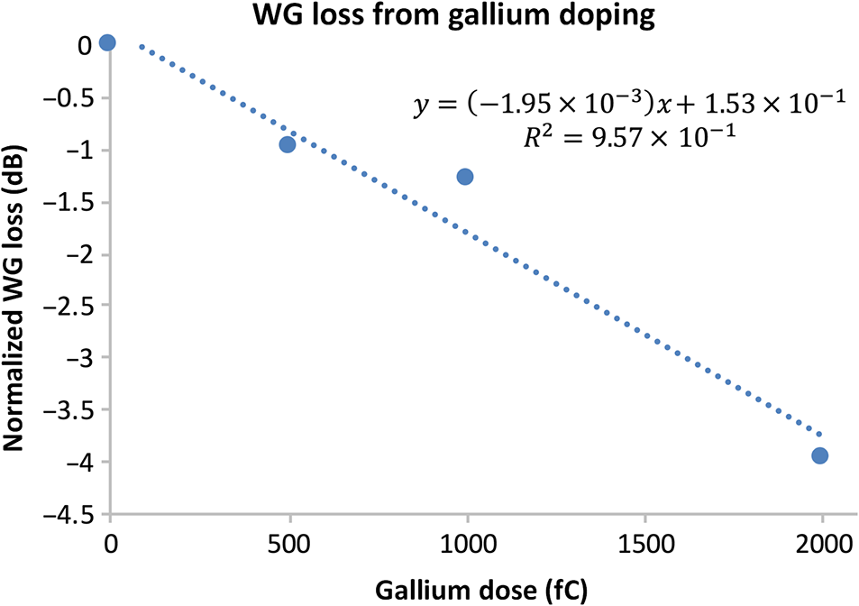
4.Results and DiscussionPolymer WG prototypes were evaluated to observe propagation loss of an optical signal through the milled taper end-face. An SM fiber-coupled laser diode source () was used as an input source. The power was polarization-adjusted using manual fiber polarization controllers (Thorlabs, Inc.) to ensure TE-polarized output for minimum plasmonic coupling with the gold substrate. IR power was coupled with the polymer WGs and the output of polymer WG tapers was collected with a microscope objective () and measured using a germanium photodiode. The output of milled tapered WGs was measured and compared with control WGs to isolate taper loss. Measurement of polymer WGs with FIB-milled tapers could not be measured with confidence () resulting in an experimental taper loss of above the measured 9 dB in polymer WG loss. Two main sources of loss due to the milling process are hypothesized. Ion beam interaction with the gold-coated substrate resulting in gold redeposition could occur at both the taper sidewalls and the taper end-face during horizontal tapering. Additionally, vertical tapering would induce a limited amount of ions to be implanted within the polymer WG allowing for higher levels of absorption and scattering. Utilizing energy dispersive spectroscopy (EDS) under a scanning electron microscope (SEM), a qualitative evaluation of material presence can be obtained within a selected scanning region. While EDS is not suitable for quantitative analysis of elemental percentages, it allows for rough evaluation to detect relative percentage levels of elements on imaged samples. EDS analysis on horizontal taper sidewalls did demonstrate high levels of gallium and gold, as shown in Fig. 12. Attempts to mill off a thin sheet of taper sidewall resulted in an increase in metallic impurities at the taper sidewalls. While Si is also present at taper sidewalls it is difficult to determine how much is due to redeposition as the polymer material is siloxane-based (). Additionally, vertical tapering resulted in a high () percentage of gallium on the top sides of etched polymer tapers. Fig. 12(a, c) EDS analysis of (b) polymer taper showing the presence of gold and gallium on FIB taper. 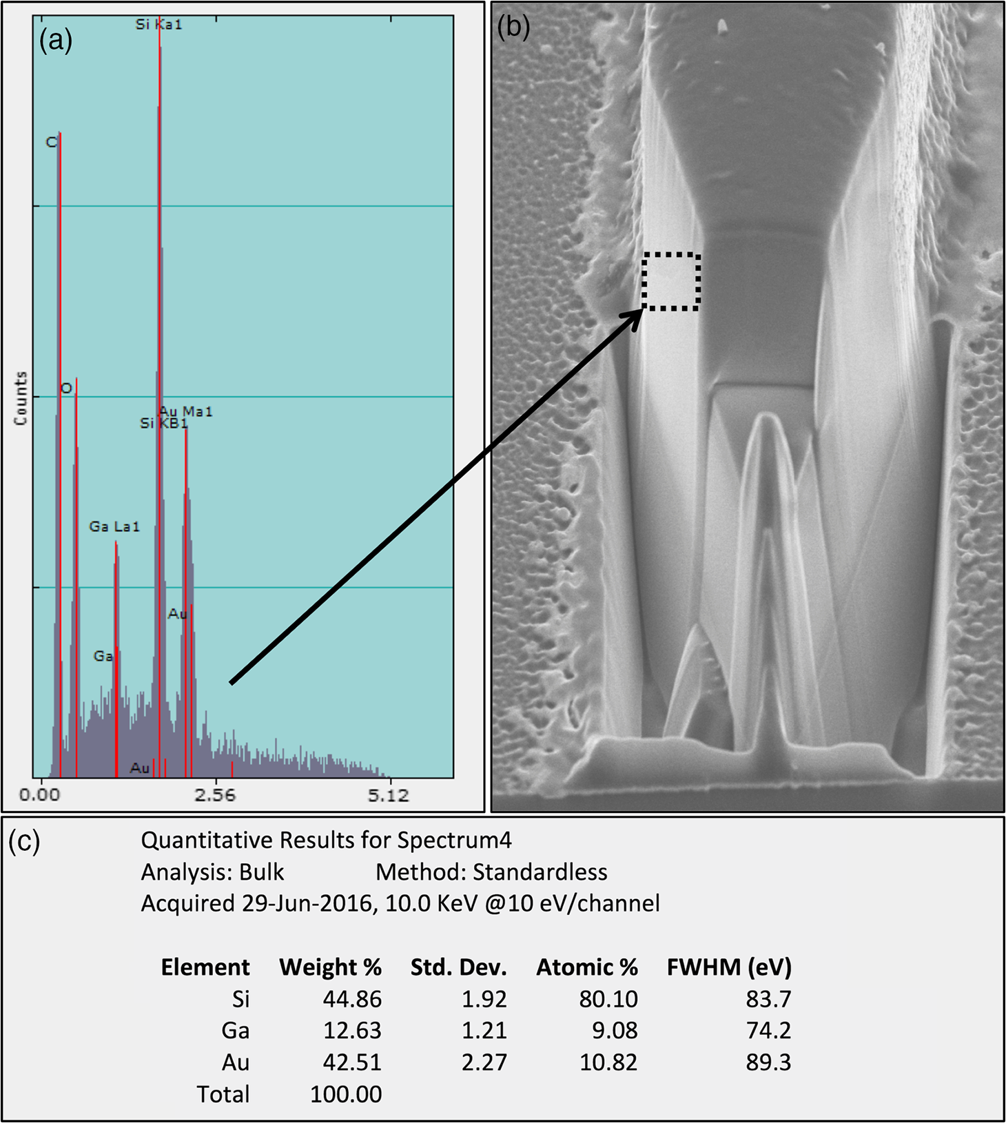 To experimentally test the effects of metal redeposition on WG sidewalls, polymer WGs were milled with horizontal tapers (, ), as shown in Fig. 13. Polymer WGs with horizontal tapers etched into them experienced an additional 8.7 dB of loss. Extrapolating these experimental results leads to an expected taper loss of 14.9 dB. Fig. 13Illustration of horizontal etched WGs to test loss effects from metal redeposition on WG sidewalls. 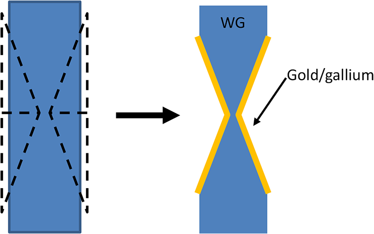 The main cause of high taper loss comes from gallium doping as a result of ion beam interactions with the polymer material. ions from the milling beam become imbedded within the milled substrate resulting in doping and partial metallization. Ionization and thermal agitation result in both chemical and morphological changes to the surrounding region. Thus the ion beam causes irreversible damage to the sample. Lehrer et al.6 has stated that as much as 10% of the ion beam becomes embedded within the substrate during the milling process with the concentration decaying exponentially deeper into the medium up to depths of . Additional authors have stated that gallium doping can lead to extremely high levels of absorption/scattering loss ().7,8 Polymer WGs were lightly milled to induce varying levels of gallium doping to observe optical losses as a function of etch dose, as shown in Fig. 14. Unlike the length-dependent loss factor associated with metallic extinction from the bottom cladding, losses due to implantation appear to be independent of distance and instead vary directly with total energy dosage as the FIB interacts with the polymer. While the milling does introduce a certain level of dimensional mismatch at the boundaries of the etched region (height mismatch of for a 2000 fC dose) its effect is marginal in comparison to the observed WG loss shown in Fig. 15. Extrapolating experimental observations would result in taper loss of over 100 dB, further reinforcing the difficulty of measuring device performance and identifying actual losses from the FIB-milled taper. Milling the majority of the material at the taper end-face would result in extreme accumulation of gallium ions and metallic precipitation would occur, overshadowing the transparent properties of the polymer material. Loss requirements are highly application-specific as certain optical modulators and amplifiers allow for loss budgets in excess of 30 dB. For most purposes, however, alternative methods must be sought to acquire low-loss tapers for high-throughput processing with the FIB inducing such high optical losses within the polymer WG tapers. To avoid gallium contamination, polymer tapers can be fabricated with one-step procedures utilizing master molds, thus eliminating alignment-based processing steps, improving taper sidewall roughness, and decreasing overall design costs. Vertical tapers manufactured with 25 nm RMS sidewall roughness would theoretically exhibit device loss of 1.1 dB as a result of gold absorption (1.0 dB) and scattering (0.1 dB, 25 nm RMS). Soft imprint lithography9,10 is a high-resolution (), high-throughput molding technique for polymer materials that exhibit thermoplastic characteristics, though incompatibility exists with complex network polymers that exhibit a high degree of cross-linking.4,11,12 Step-and-flash imprint lithography has been shown to be a reliable method for molding complex polymer materials at submicron resolution through the use of a transparent mold.13 Alternatively, UV-initiated WG polymers can be uniformly UV cured, pressed into the desired taper shape, and then thermally cured to complete polymerization without requiring a transparent mask.14 Utilizing these manufacturing methods, optimal polymer taper loss can be minimized by optimizing polymer taper dimensions and minimizing fabrication noise. Master molds for these methods are built on Si using CMOS-compatible procedures (photolithography and reactive-ion etching) with PDMS being utilized as a pattern transfer material for polymer imprinting. While horizontal tapers can be processed lithographically vertical taper fabrication is significantly more complex. Vertical tapers can be formed through shadow mask15 or grayscale16 etching techniques. There is also potential for the FIB milling technique to be exploited by using its high-precision etching capabilities to manufacture a mold without susceptibility to gallium implantation or gold redeposition in the final molded tapers. 5.Waveguide Taper: ConclusionPolymer WG tapers are vital in optimizing data transmission rates and coupling efficiencies between Si photonic interconnects and SMFs. The fabrication of polymer WG tapers was conducted utilizing the FIB to acquire high resolution ( RMS) requirements necessary for low scattering loss. The etch rate of polymer WGs with the FIB was calibrated and measured at when a pixel spacing of 50.47 nm was utilized. Additionally, practical understanding of FIB interactions with nonplanar surfaces was discussed to optimize milling procedures in producing polymer WG tapers. Experimental testing observed polymer tapers to exhibit high () taper loss due to metallic redeposition on the taper sidewall and gallium ion implantation within the polymer WG. AcknowledgmentsThe authors wish to thank Molex for funding this research under Michigan Tech Contract No. 1505001. The authors gratefully acknowledge use of the services and facilities of the Applied Chemical and Morphological Analysis Laboratory (ACMAL) located at Michigan Technological University. ReferencesM. C. Teich and B. Saleh, Fundamentals of Photonics, 3 Wiley Interscience, Canada
(1991). Google Scholar
J. Galán, P. Sanchis and J. Martí,
“Low-loss coupling technique between SOI waveguides and standard single-mode fibers,”
Opt. Express, 15
(11), 7058
–7065
(2007). Google Scholar
K. Kruse and C. T. Middlebrook,
“Polymer taper bridge for silicon waveguide to single mode waveguide coupling,”
Opt. Commun., 362 87
–95
(2016). http://dx.doi.org/10.1016/j.optcom.2015.08.079 JLTEDGOPCOB8 0733-87240030-4018 Google Scholar
D. A. Chang-Yen, R. K. Eich and B. K. Gale,
“A monolithic PDMS waveguide system fabricated using soft-lithography techniques,”
J. Lightwave Technol., 23 2088
–2093
(2005). http://dx.doi.org/10.1109/JLT.2005.849932 Google Scholar
A. A. Tseng,
“Recent developments in micromilling using focused ion beam technology,”
J. Micromech. Microeng., 14 R15
(2004). http://dx.doi.org/10.1088/0960-1317/14/4/R01 JMMIEZJMMIEZ 0960-13170960-1317 Google Scholar
C. Lehrer et al.,
“Defects and gallium-contamination during focused ion beam micro machining,”
in Conf. on Ion Implantation Technology,
695
–698
(2000). Google Scholar
J. Schrauwen, D. Van Thourhout and R. Baets,
“Focused-ion-beam fabricated vertical fiber couplers on silicon-on-insulator waveguides,”
Appl. Phys. Lett., 89 141102
(2006). http://dx.doi.org/10.1063/1.2356311 APPLAB 0003-6951 Google Scholar
R. M. De Ridder, W. C. Hopman and F. Ay,
“Focused-ion-beam processing for photonics,”
in 9th Int. Conf. on Transparent Optical Networks (ICTON 2007),
212
–215
(2007). Google Scholar
C. Pina-Hernandez, L. J. Guo and P.-F. Fu,
“High-resolution functional epoxysilsesquioxane-based patterning layers for large-area nanoimprinting,”
ACS Nano, 4 4776
–4784
(2010). http://dx.doi.org/10.1021/nn100478a ANCAC3 1936-0851 Google Scholar
C. Pina-Hernandez, P.-F. Fu and L. J. Guo,
“Ultrasmall structure fabrication via a facile size modification of nanoimprinted functional silsesquioxane features,”
ACS Nano, 5 923
–931
(2011). http://dx.doi.org/10.1021/nn102127z ANCAC3 1936-0851 Google Scholar
B. D. Gates and G. M. Whitesides,
“Replication of vertical features smaller than 2 nm by soft lithography,”
J. Am. Chem. Soc., 125 14986
–14987
(2003). http://dx.doi.org/10.1021/ja0367647 JACSAT 0002-7863 Google Scholar
F. Hua et al.,
“Polymer imprint lithography with molecular-scale resolution,”
Nano Lett., 4 2467
–2471
(2004). http://dx.doi.org/10.1021/nl048355u NALEFD 1530-6984 Google Scholar
M. Colburn et al.,
“Step and flash imprint lithography: a new approach to high-resolution patterning,”
Proc. SPIE, 3676 379
–389
(1999). https://doi.org/http://doi.dx.org/10.1117/12.351155 Google Scholar
H. Lorenz et al.,
“SU-8: a low-cost negative resist for MEMS,”
J. Micromech. Microeng., 7 121
–124
(1997). http://dx.doi.org/10.1088/0960-1317/7/3/010 Google Scholar
S. M. Garner et al.,
“Three-dimensional integrated optics using polymers,”
IEEE J. Quantum Electron., 35 1146
–1155
(1999). http://dx.doi.org/10.1109/3.777214 IEJQA7 0018-9197 Google Scholar
A. Sure et al.,
“Fabrication and characterization of three-dimensional silicon tapers,”
Opt. Express, 11 3555
–3561
(2003). http://dx.doi.org/10.1364/OE.11.003555 OPEXFF 1094-4087 Google Scholar
BiographyKevin Kruse received his PhD in electrical engineering with a concentration in photonics from Michigan Technological University in 2015. He has had over 5 years of experience in the design, simulation, fabrication, and evaluation of optical waveguides for both academia and industry. His career interests are in optical communication, optoelectronic and photonic devices, and microfabrication. Derek Burrell is an undergraduate student studying electrical engineering with a concentration in photonics at the Michigan Technological University. He has developed procedures for the fabrication and testing of optical interconnects, designed photometric simulations, and created light-based models for virtual reality systems. He has been employed as an intern for Molex Corp. and OPTIS and has received a prestigious SPIE Optics and Photonics Education Scholarship. His research interests include telecommunications, digital image processing, and materials characterization. Christopher Middlebrook is an associate professor of electrical and computer engineering at the Michigan Technological University. He has an active research program in photonics and optics specializing in integrated photonic devices, material characterization for optical applications, microwave photonics, visible and infrared imaging systems, optical remote sensing system design, and laser projection systems. Current research topics focus on polymer optical waveguides for high speed computing applications, microwave photonic devices and applications, and speckle reduction techniques. |