|
|
1.Motivation1.1.Reliability of Micro-(Opto)-Electro-Mechanical-System DevicesThe characterization of a micro-(opto)-electro-mechanical-system device [M(O)EMS] includes the investigation of mechanisms that lead to device failure, as well as the description of changing device characteristics during a degradation process far below the level that leads to catastrophic failure. An overview of common MEMS design elements and their related failure mechanisms for metals and brittle materials is presented in Ref. 1. Therein, Spengen specifies several mechanisms including: creep, fracture, stiction, electromigration, wear, and the degradation of dielectrics. In the field of MEMS mirror devices, degradation mechanisms leading to nonfunctional (sticking) mirrors caused by repeating operation cycles or by environmental conditions typically include hinge memory, hinge fatigue, particulate contamination, surface residue, or capillary condensation.2,3 The present work investigates degradation introduced by laser irradiation within the intended operating limits. The literature in this field is rather limited, with existing works often focusing on the laser damage threshold rather than on degradation mechanisms far below this threshold.4,5 Bowing and the deformation of optical surfaces and other actuator elements (springs, supports) is one type of degradation occurring at lower power levels.6 At higher power levels, metallic coatings tend to show a loss of reflectivity possibly resulting from degradation in terms of surface roughening, agglomeration or complete ablation of the coating material.4 In addition, laser-induced charge trapping in dielectric layers presents yet another challenge in that trapped charges may seriously impact the performance of devices operating according to electrostatic principles.7,8 1.2.Spatial Light Modulators for MicrolithographyThe Fraunhofer Institute for Photonic Microsystems (FH-IPMS) develops spatial light modulators (SLMs) based on arrays of micromirrors (Fig. 1). Such SLMs have become an established technology, e.g., in the field of microlithography. Utilized as reflective, programmable photomasks in deep-UV mask writers, they enable highly flexible pattern generation.9–12 Another application of IPMS-SLMs in microlithography, laser direct imaging, uses a high-speed one-dimensional SLM for processing advanced substrates for semiconductor packaging.13 Fig. 1Photograph of the IPMS-SLM investigated within the present experiment with (a) SLM bonded into a ceramic package and (b) scanning electron microscope-image of a collection of single micromirrors with mirror pitch. 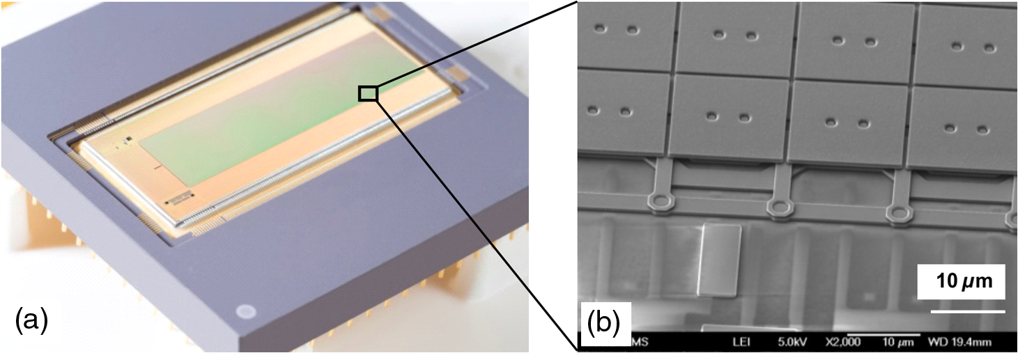 During SLM operation, the micromirror bow has a significant impact on the contrast and on the resolvable feature size of the patterns generated.14 Demanding specifications regarding mirror planarity for SLMs used in microlithography applications are therefore needed. These specifications include the initial planarity at the beginning as well as the allowable change during operation. The analysis of micromirror planarity has been a standard tool of process control in SLM fabrication for many years. However, in the past, the analysis of mirror topology was conducted only in a separate step, following the irradiation. Providing in situ analysis parallel to normal operation allows a direct evaluation of the effects of different irradiation parameters (such as laser fluence, laser wavelength, laser repetition rate, and purging gas) on micromirror topology. 2.Method2.1.SampleThe SLM characterized in the present study is a two-dimensional array of on a pitch. Each pixel is composed of a mirror plate mounted on two posts onto a separate layer of torsional springs. The mirrors can be tilted about an axis through the torsional springs by the electrostatic principle. For this purpose, a voltage is applied between the mirror plate and underlying electrodes (Fig. 2). An underlying CMOS circuitry allows an individual control of each pixel.9,15 The mirror plate and torsional springs are realized in two independent metallization layers, allowing for the use of different materials. The mechanical and optical properties of springs and reflector can therefore be optimized independently from each other. Fig. 2Design of one-axis tilting mirror with (a) mirror plate and (b) design of mechanical and electrical components allowing the mirror actuation (torsional springs with yoke and electrodes underneath).  It should be mentioned that the SLM investigated in this experiment was not designed for high-intensity irradiation. The energy level applied during the experiment was orders of magnitudes higher than the level, which is used in its intended application. The intense optical load was placed on the sample to provoke measurable sample reaction and to investigate possible limitations of applications. 2.2.In Situ Measurement of Mirror Bow by Phase-Shift InterferometryAs single-mirror curvature affects the imaging behavior and the contrast of the generated patterns, the present work focuses on the main question of what effect UV-laser light has on mirror curvature. The measurand “bow” is used to characterize this curvature; it is the height of a circular segment fitted to the mirror surface profile. In this work, two bow values are reported, each resulting from fitting a cylinder to the three-dimensional (3-D) surface with the axis orientated along the mirror edges [Fig. 3(a)]. Fig. 3In situ analysis of micromirror bow with (a) definition of the measurand “bow” and (b) experimental setup with excimer laser (KrF), attenuator, optics for beam guiding and beam shaping, phase-shift interferometer, vibration isolated optical table and housing. 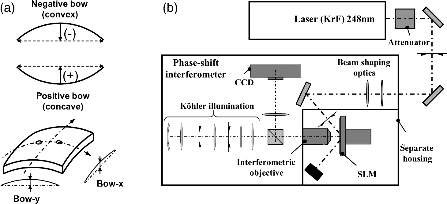 Phase-shift interferometry (PSI) delivers the in situ detection of mirror curvature during the laser exposure, with the required accuracy in the nanometer range. A very sensitive contact-free optical measurement principle for 3-D surface characterization, PSI allows a resolution in -direction in the range of .16 The concept of the experimental setup illustrated below shows an excimer laser (KrF) emitting at 248 nm, an attenuator for the adjustment of pulse energy, UV-optics for beam guiding and beam shaping, a vibration isolated optical table, the interferometer and housing to protect said interferometer from ambient conditions [Fig. 3(b)]. In normal operation, the SLM is often irradiated perpendicularly (0 deg angle of incidence). As the present experimental setup combines laser irradiation and interferometric measurement, the laser’s incidence angle must be changed to 55 deg to fit in the two separate optical paths. This results in a decrease of mirror reflectance from 91% to 88% when compared to normal operation. 2.3.Procedure of Data Acquisition and AnalysisThe characterization of such a complex device raises the question of whether the results show typical properties of the investigated mirror material or whether they show the specific behavior of just a few investigated samples. Although it is nearly impossible to totally eliminate device-dependent results, they must be kept to a minimum. For this purpose, a study was conducted prior to the actual experiment to determine general parameters and experimental conditions that have an impact on the detected mirror bow. Furthermore, each particular measurement series was carried out several times and cross-checked by using different samples. During the investigation of the effect of a certain irradiation parameter (e.g., the pulse energy), only samples from the same fabrication batch were used. All in all, more than 20 devices were analyzed within the experiment. After data acquisition, a commercially available, interferometric analysis software (IntelliWave™) is used to calculate the sample height map. A typical optical path difference (OPD) map, resulting from this analysis, is presented here [Fig. 4(a)]. This topology map is then passed through another image processing software to recognize each single mirror within this pattern and to separate the mirror surfaces from surrounding slits and post holes [Fig. 4(b)]. Fig. 4Contact-free measurement of micromirror topology in the nanometer scale with (a) optical path difference (OPD) map of a selection of mirrors (derived from the interferometer’s intensity data) and (b) clearance cutting of each single mirror and separation from the surrounding mirror slits and post holes. 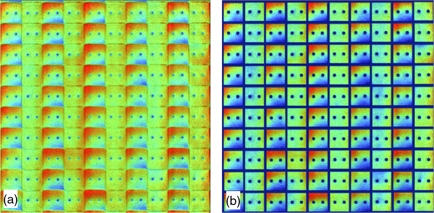 This necessary step eliminates disturbing spikes in the height profile that result from light reflected out of slits and holes. Finally, an automated fitting routine individually fits each of the mirror surfaces. One can then derive statistical information about the average mirror bow and the spread in values. 2.4.Procedure of Single and Multiple Measurement CyclesFigure 5 provides an introduction to the general measurement procedure. While Fig. 5(a) illustrates a single measurement cycle, Fig. 5(b) shows a series of five irradiation cycles. As depicted in Fig. 5(a), a single measurement cycle consists of three periods, including the data acquisition before (I), during (II), and after (III) the laser irradiation. Both periods II and III have a duration of 1 h. The -axis charts the average bow change (measured in nanometers), for a selection of 500 mirrors. The bow measured prior to the first irradiation cycle is defined as zero, the initial state. The -axis plots the number of applied pulses. After , irradiation is stopped, however, bow measurement continues until . Fig. 5Introduction of the measurement procedure with (a) procedure of a single measurement cycle with bow analysis before (I), during (II), and after (III) the laser irradiation and (b) procedure of a series of five irradiation cycles at constant sample position and constant measurement conditions. 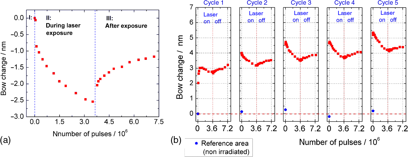 For a better understanding of the bow change in the longer run, five of these irradiation cycles were carried out one after another with a 1-day break between each cycle [Fig. 5(b)]. As irradiation conditions and sample position were kept constant during each series, subsequent cycles show the real bow change with respect to the first cycle. Before each cycle, a nonradiated reference area was measured to monitor the effect of ambient conditions on measurement accuracy. A detailed description of the experimental setup, an analysis of measurement error and an explanation of the measurement procedure are provided in Ref. 17. 3.Results3.1.Mirror Bow as a Function of Energy DensityThe following section describes the mirror bow change as a function of different irradiation parameters: energy density, deposited energy, and pulse number and also discusses the effect of laser-induced heating. To investigate the bow as a function of the applied energy density, samples were irradiated within the range of to . The lower value was chosen as the minimum level at which a laser-driven bow change was observed at all in the sample, the upper value was limited by the maximum pulse energy attainable in this experimental setup. Table 1 further summarizes other irradiation parameters during the experiment. Table 1Irradiation parameters applied during the investigations of mirror bow as a function of pulse-energy density
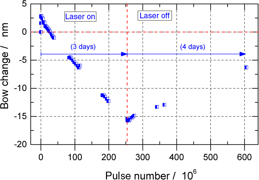
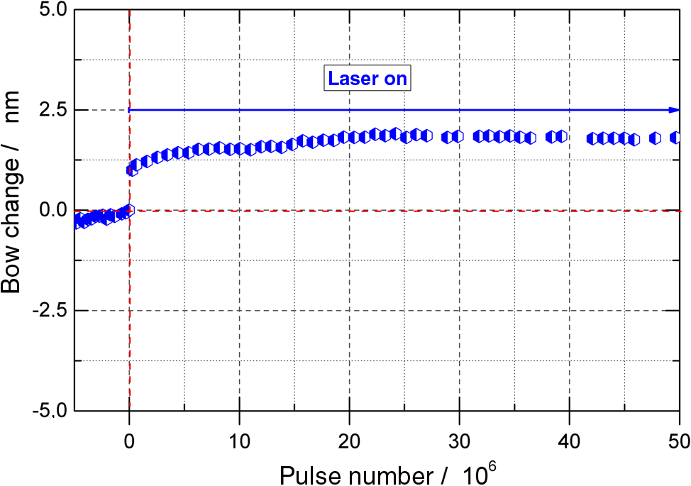
Lower energy levels of up to produce a cumulative change of the bow in the positive (concave) direction [Fig. 6(a)]. The majority of the bow change occurs during the first irradiation cycle and subsequent cycles follow the same tendency. When irradiation is stopped, mirrors show hardly any relaxation and even continue bowing slightly in the same direction as before. Therefore, the detected bowing is defined as one of a permanent manner. Over the whole series, the positive bow change adds up to 0.5, 2, and 4 nm, respectively. Fig. 6Analysis of micromirror bow as a function of the applied pulse-energy density with (a) bow change at “lower” energy levels ( to ) and (b) bow change at “higher” energy levels (10 to ). 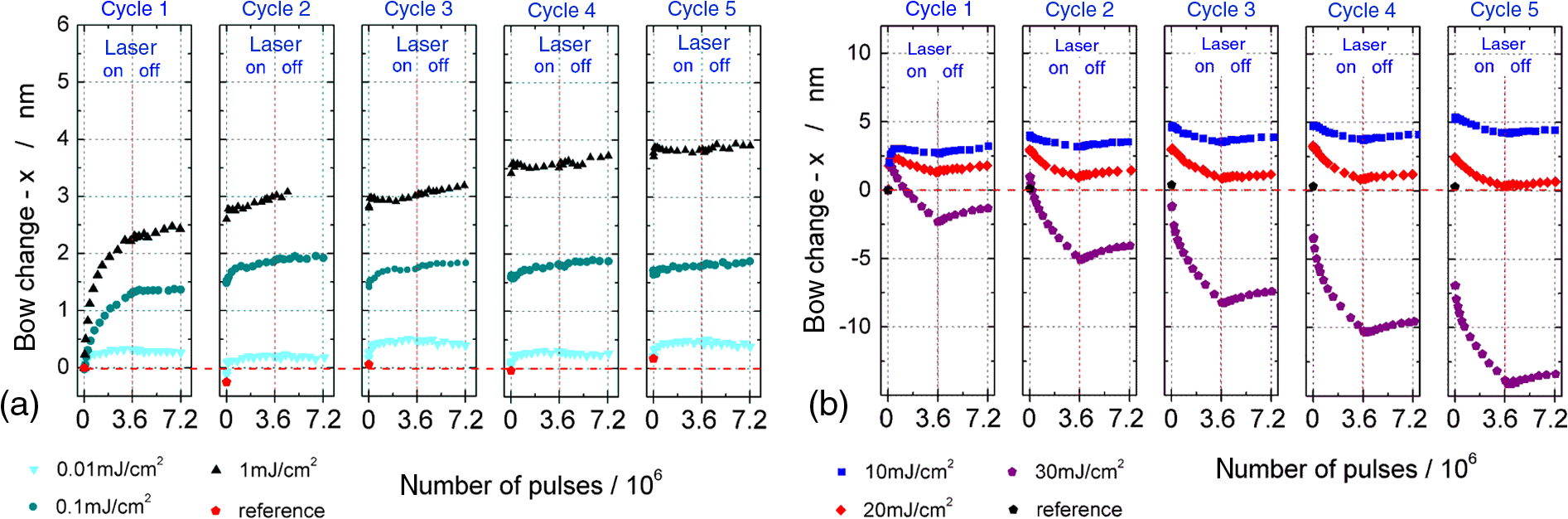 As illustrated [Fig. 6(b)], we see that in cycles using energy levels above , bowing during irradiation can differ significantly from bowing after irradiation has stopped. Bowing during the first irradiation cycle is different compared to the following cycles. Within a couple of hundreds of thousands pulses, the mirrors show a rapid positive bow change. However, after this initial phase, while the irradiation is ongoing, the initially positive direction of bow change turns negative. The higher the applied energy level, the quicker the turn around and the stronger the following negative change. Depending on the applied energy density, this negative change adds up to , , and , respectively, within the first . When the irradiation is stopped, the bow then slightly relaxes toward the initial value. This relaxation adds up to about 1 nm within the first hour. After each of the subsequent cycles, the bow becomes progressively more negative as compared to the starting state. The fact that the change in bow (at the higher energy levels) is composed of two parts with different signs and timescales indicates the presence of two different driving mechanisms behind the observed behavior. One mechanism is assumed to cause the same permanent positive bow change as is observed at energy densities up to . The other is assumed to cause the bow change in negative direction, an effect that is observed only at higher energy levels. 3.2.Mirror Bow as a Function of Deposited Energy (Over Shorter Time Scales)The results presented in Fig. 6 have indicated that unirradiated mirrors go through a unique conditioning process during their first irradiation cycle. Figure 7 presents the bow change as a function of the deposited energy using information derived from Fig. 6 and using energy rather than pulse number on the -axis. Depending on the applied energy density, the different curves represent varying pulse numbers, but always the same deposited energy. As a consequence, the curve shows more than the first irradiation cycle for the case, but only a fraction of the first cycle for the case (hence the negative trends seen later in the high energy irradiations are not included). All curves depicted (energy densities) show a similar bow change within the deposited energy of . The further deposition of up to has almost no effect on the bow. These results confirm the assumption of a conditioning process, possibly arising from a permanent change of mirror material properties, completed at a deposited energy of about . Fig. 7Micromirror bow change during a UV-laser irradiation as a function of the deposited energy at rising pulse-energy densities from 1 to (data is extracted from the datasets presented earlier in Fig. 6). 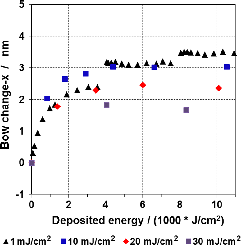 3.3.Bow Change Over Longer Time ScalesThe following section analyzes the bow change during a long-term irradiation. The sample was exposed to (at ), as compared to during the former series. Contrary to the previous procedure, the sample was submitted to a continuous irradiation for three days, with only a few short interruptions for laser gas exchanges. Longer gaps within the curve (Fig. 8) occurred at night when the data collection was paused, but irradiation itself was still ongoing. As seen previously during the short-term irradiations, first, mirrors show a rapid bow change for a couple of hundreds of thousands pulses in the positive direction, followed by said inversion in the direction of bowing. From that point on, there is a steady bow change in the negative direction until the irradiation is stopped. Within the period, the bow change sums up to . When the irradiation is stopped, the mirror bow slowly relaxes over several days. After 4 days, the initial bow change was relaxed by about 50%. Long-term irradiation revealed that the positive bow change at the beginning is a rather small effect, which does not have much relevance in the long run. For irradiations exceeding several hundred million pulses and beyond, the negative bow change is the limiting factor for energy densities above the level. The question is: which mechanism is behind such a long-term behavior? 3.4.Laser-Induced HeatingThe following section analyzes the micromirror temperature during a pulsed laser irradiation. The measurement is based on the detection of the temperature-dependent ohmic resistance of an electric conductor. Many mirrors are connected in a chain to form an ohmic resistor and a four-terminal sensing is applied to detect the change of the temperature-dependent resistance of the irradiated mirrors (Fig. 9). Prior to measurement, a test section must be calibrated by means of a precision oven to determine the resistance-temperature curve. The laser-induced effect on mirror temperature is then determined using the four-terminal sensing technique. As illustrated [Fig. 9(b)], a constant current is applied along the yellow path and the temperature-dependent voltage is detected between the green contacts using an oscilloscope, which allows the resolution of short-time scale changes on the microsecond scale. Mirror temperature is ultimately determined by using the fit function of the resistance–temperature calibration curve. The sample preparation and measurement principle are discussed in more detail in Refs. 17 and 18. Fig. 9In situ analysis of micromirror temperature during a UV-laser irradiation by means of a four-terminal sensing with (a) rows of micromirrors connected to an ohmic resistor and (b) layout of the four-terminal sensing.18 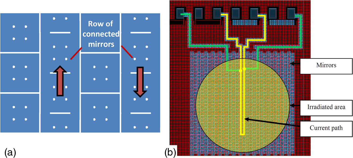 First, the temperature change following a single-laser pulse was analyzed. Therefore, the test section was irradiated at increasing energy densities from 0.1 up to . It has to be mentioned that each of the presented curves [Fig. 10(a)] depicts the average of 64 events (pulses) to reduce the measurement noise level. At the lowest level of , the mirror temperature shows no significant response to the incoming pulse. The maximum level of results in a peak value of 117 K. Rise and fall times were derived from the curve to provide a quantitive description of the time response. The rise time from the 10% to the 90% level equals . The fall time from to the level equals . Fig. 10In situ analysis of mirror temperature during a UV-laser irradiation with (a) rise of mirror temperature introduced by single-laser pulses at varying pulse-energy densities (0.1 to ) and (b) analysis of the time-averaged mirror temperature during a long pulse train at varying pulse-energy densities (5 to ). 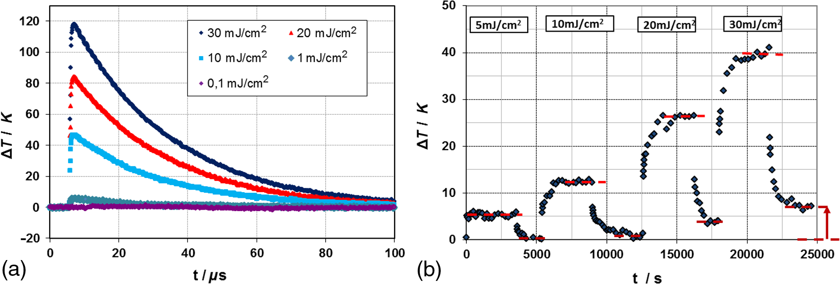 Next, the temperature change during a longer pulse train was analyzed. In this case, a single data point represents the time-averaged temperature over many pulses [Fig. 10(b)]. During the course of the measurement series, the sample was irradiated continuously for 1 h at a given energy level, followed by an interruption of 30 min and then progression to the next energy level. The detected temperature changes are measured as 5, 12, 26, and 34 K, respectively, depending on the irradiation pulse energy. The timeframe needed until the irradiated section reached a thermal equilibrium is unexpectedly long. Above , it takes more than 15 min until the temperature has leveled out. It is assumed that such a course arises from the gradual temperature change in the underlying material layers (substrate). The final “laser off” level at the end, where temperature seems to remain several Kelvin above room temperature is also remarkable. It is assumed that this effect is caused by a permanent modification of the grain structure and ohmic resistance of the irradiated mirrors. These phenomena are discussed in more detail in Ref. 17. 3.5.Laser-Induced Degradation Analysis of the Mirror Material with Transmission Electron MicroscopyCross-sectional transmission electron microscopy (TEM) studies were performed to correlate the variation of optical and mechanical properties during laser irradiation with microstructural changes, in particular with the mirror grain and the mirror surface structure. For this purpose, a sample exposed to at was compared to a nonirradiated reference mirror. TEM lamella preparation was done by in situ lift-out using a Zeiss Crossbeam NVision 40 system at the Helmholtz–Zentrum Dresden–Rossendorf (HZDR). To protect the sensitive surface of the area of interest, a carbon cap layer was deposited, beginning with electron-beam-assisted and subsequently followed by Ga-focused-ion-beam (FIB)-assisted precursor decomposition. Afterward, the TEM lamella was prepared using a 30-keV Ga FIB with adapted currents. Its transfer to a three-post copper lift-out grid (Omniprobe) was achieved with a Kleindiek micromanipulator. To minimize sidewall damage, Ga ions with only 5-keV energy were used for the final thinning of the TEM lamella to electron transparency. TEM investigations were conducted using an image-corrected Titan 80-300 microscope (FEI) at HZDR. In addition to bright-field imaging, high-resolution TEM (HRTEM) micrographs were also obtained to analyze the grain and surface structure of the Al-based mirrors. Mounted in a double tilt analytical holder, the specimen was placed for about 30 s into a Model 1020 Plasma Cleaner (Fischione) to remove organic contamination prior to TEM analysis. This example (Fig. 11) shows a cross-sectional bright-field TEM image of the mirror setup consisting of the mirror plate, the mirror post, and the torsional spring below. Fig. 11Cross-sectional bright-field TEM overview micrograph of the nonirradiated specimen showing the mirror plate, the mirror post and the torsional spring below. The mirror surface is covered by a carbon protection layer deposited during TEM lamella preparation. 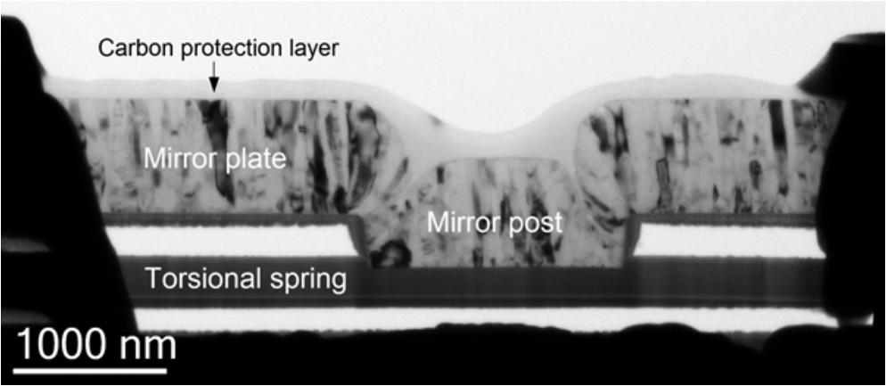 For comparison of the grain structure, further examples show bright-field TEM images of the mirror plate before and after laser irradiation, respectively [Figs. 12(a) and 12(b)]. During mirror fabrication, the Al-alloy (mirror plate) was deposited onto a sacrificial layer (), which is removed in a later process step. The top and bottom sides of the mirror plate are oxidized, as evidenced by the presence of a thin homogeneous light-gray layer [Fig. 12(a)]. With a height of a few nanometers, the oxide layer is about as thick as naturally grown aluminum oxide. Underneath the bottom oxide layer, there is another inhomogeneously structured film of about 60-nm thickness. This layer consists of material redeposited onto the unprotected backside of the mirror plate during FIB lamella preparation. The mirror plate (Al-alloy) itself shows columnar grain growth with grain diameters of and grain heights up to the mirror thickness of 730 nm, whereupon grain nucleation and growth selection occurs within the first 100 nm. When comparing the samples that represent the mirror state before and after irradiation, there are no significant changes in grain shape or grain size visible [Fig. 12(b)]. Fig. 12Bright-field TEM micrographs comparing the mirror plate grain structure for (a) the nonirradiated specimen and (b) after laser irradiation with at . 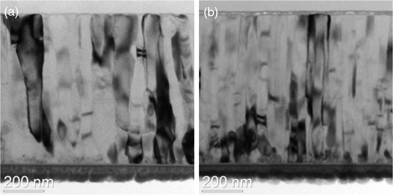 Most metallic surfaces such as aluminum develop a naturally grown oxide layer when coming into contact with atmospheric oxygen. Visible in the bright-field TEM image [Fig. 13(a)] as a homogeneous light-gray film at the mirror surface, this -thick oxide is of amorphous structure. High-resolution images [inset Fig. 13(a)] confirm this observation. Fig. 13Bright-field TEM micrographs and HRTEM images as inset comparing the mirror surface oxide layer for (a) the nonirradiated specimen and (b) after laser irradiation with at . 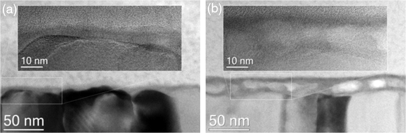 After laser irradiation, the thickness of oxide on the top side of the mirror has increased significantly. The postexposure thickness is in the range of 15 to 20 nm [Fig. 13(b)]. In addition, the laser-irradiated mirror shows pore formation within the surface oxide. The bright areas are indicative of regions of reduced mass contrast. Hence, the pores are empty or filled with a low-density material. In addition to the pores, small dark spots within the surface oxide are observed in the bright-field TEM micrograph [Fig. 13(b)], hinting to the presence of crystalline inclusions. Lattice fringes observable in the HRTEM image [inset Fig. 13(b)] confirm this observation. The irradiation seems not to have an effect on the bottom-side oxide layer. Thickness and structure of the bottom oxide do not show significant changes [Fig. 12(b)]. The consequence of the unequal oxide growth is an asymmetry in the mirror layer composition caused by the irradiation. 4.DiscussionThe laser irradiation at 248 nm of the micromirrors presented in this work shows that a minimum pulse-energy density of is required to detect any laser-induced change of the mirror bow. The detected bowing can, in principle, occur in both directions (positive/concave and negative/convex). The mechanism behind the particular bowing is sensitive to the applied irradiation parameters such as pulse-energy density, deposited energy, and pulse number. The analysis of bow change as a function of the deposited energy (Fig. 7) shows that for these test structures there is a positive bow change occurring during irradiation up to a deposited energy of some . The effect is observed for all of the pulse-energy densities tested, but it is particularly notable that it occurs for pulse-energy densities up to , where a laser-induced heating of the mirrors can be neglected. Within the said range of deposited energy, the positive bow change sums up to about . After the irradiation is stopped, the bow remains more or less stable, and a relaxation is not observed. This forms the hypothesis that such a permanent positive bowing arises from the irradiation-induced oxide formation on the upper mirror side. The modification of the mirror top oxide layer might result in a stress gradient, which forces the mirror to curve. Irradiation at “higher” pulse-energy densities () results in an additional negative (convex) bow change. When irradiation is stopped, the bow partially relaxes toward the initial value. Within a period of and for a pulse-energy level of , the bow change of these test structures sums up to a change of , hence this is the dominating effect in the long run (Fig. 8). An explanation for the observed bowing at higher energy levels might be the laser-induced increase of the mirror temperature [Fig. 10(a)]. The pulsed increase of mirror temperature reaches a level of some tens of Kelvins and beyond. It is assumed that at the moment where the pulse arrives, there is a short-term thermal gradient between mirror top and bottom, which might be significantly higher than the measured temperature rise itself. This leads to the hypothesis that each individual laser pulse introduces a temporary bimorph effect that acts as a driving force, in turn forcing the mirrors to bend. Accordingly, the mirror bowing would in fact occur rather dynamically (pulsed) than statically. Such a dynamic bowing induced by the individual laser pulses cannot be time-resolved with the current measurement setup. The interferometer used in this work averages the bow values over a time span equivalent to 100 laser pulses. Consequently, the detected bow data represent a time-averaged bowing. A more detailed discussion of the hypothesis of dynamic bowing is presented in Ref. 17. 5.ConclusionThe laser-induced bow change of micromirrors, belonging to the particular design of SLM, during an irradiation at 248 nm can roughly be separated into two distinct components: a permanent concave bowing at “lower” pulse-energy levels and a (partly) reversible convex bowing at “higher” energy levels. Irradiation with pulse-energy densities up to results in a slight concave bowing in the range of . Such a bowing, including the resulting effect on image quality, may be acceptable for most of the current SLM applications. A certain preirradiation of the SLM could even be applied to minimize the subsequent changes in mirror bow during operation of the SLM. The situation appears to be different at higher energy levels. For pulse-energy densities above the level, the laser-induced temperature rise becomes increasingly influential and causes a progressive convex bowing. Over a time span of , this mechanism sums up to a change in surface bow of about and, therefore, might have the potential to become a limiting factor in SLM operation. For a successful implementation of SLM design used for this work, at energy levels of or higher, certain modifications in the micromirror design need to be made. A further improvement of the mirror reflectivity, the selection of a material that is more robust against the irradiation and using an increased mirror thickness could be promising approaches for such design advancement. 6.OutlookThe improvement of micromirror design for applications that involve higher pulse-energy levels has been part of the Fraunhofer IPMS’s current activities. As a first step, the SLM was equipped with thicker and therefore stiffer mirrors to reduce the effect of laser-induced bowing. Initial irradiation tests at show a significant improvement in the detected bowing behavior (Fig. 14). Irradiated mirrors show a bow change of just 2 nm within a couple of million pulses, followed by a stabilization of the mirror curvature around this level. Although the approach based on using thicker mirrors has some limitation, it shows promising perspectives for applications requiring the manipulation of higher power laser beams, e.g., in the laser material processing business. ReferencesW. M. van Spengen,
“MEMS reliability from a failure mechanisms perspective,”
Microelectron. Reliab., 43 1049
–1060
(2003). http://dx.doi.org/10.1016/S0026-2714(03)00119-7 PSISDGMCRLAS 0277-786X0026-2714 Google Scholar
M. R. Douglass,
“Lifetime estimates and unique failure mechanisms of the digital microimirror device (DMD),”
in IEEE 98CH36173. 36th Annual Int. Reliability Physics Symp.,
(1998). http://dx.doi.org/10.1109/RELPHY.1998.670436 Google Scholar
I. Stanimirović and Z. Stanimirović, MEMS Micromirror Arrays: Some Reliability Issues, 13 13 Infoteh-Jahorina, University of East Sarajevo(2014). Google Scholar
D. M. Burns and V. M. Bright,
“Mirrors optical power induced damage to microelectromechanical,”
Sens. Actuators A, 70 6
–14
(1998). http://dx.doi.org/10.1016/S0924-4247(98)00106-X Google Scholar
L. Phinney et al.,
“Damage of MEMS thermal actuators heated by laser irradiation,”
Proc. SPIE, 5716 81
(2005). http://dx.doi.org/10.1117/12.594408 PSISDG 0277-786X Google Scholar
O. B. Spahn et al.,
“Impact of high optical power on optical MEMS,”
in IEEE/LEOS Int. Conf. on Optical MEMS and Nanophotonics,
(2008). http://dx.doi.org/10.1109/OMEMS.2008.4607832 Google Scholar
T. F. Miyahira et al.,
“Total dose degradation of MEMS optical mirrors,”
IEEE Trans. Nucl. Sci., 50
(6), 1860
–1866
(2003). http://dx.doi.org/10.1109/TNS.2003.820764 IETNAE 0018-9499 Google Scholar
U. Dauderstädt et al.,
“Charging effects in micromirror spatial light modulators,”
J. Micro/Nanolith. MEMS MOEMS, 7
(2), 021011
(2008). http://dx.doi.org/10.1117/1.2911021 Google Scholar
L. Haspeslagh et al.,
“Highly reliable CMOS-integrated 11MPixel SiGe-based micro-mirror arrays for high-end industrial applications,”
in 2008 IEEE Int. Electron Devices Meeting,
(2008). http://dx.doi.org/10.1109/IEDM.2008.4796779 Google Scholar
J. Lauria et al.,
“SLM device for 193 nm lithographic applications,”
Microelectron. Eng.,
(2008). http://dx.doi.org/10.1016/j.mee.2008.11.022 Google Scholar
T. Sandström et al.,
“Pattern generation with SLM imaging,”
Proc. SPIE, 4562 38
(2002). http://dx.doi.org/10.1117/12.458312 PSISDG 0277-786X Google Scholar
U. Dauderstädt et al.,
“Advances in SLM development for microlithography,”
Proc. SPIE, 7208 720804
(2009). http://dx.doi.org/10.1117/12.810787 PSISDG 0277-786X Google Scholar
J. Schmidt et al.,
“High-speed one-dimensional spatial light modulator for laser direct imaging and other patterning applications,”
Proc. SPIE, 8977 89770O
(2014). http://dx.doi.org/10.1117/12.2036533 PSISDG 0277-786X Google Scholar
J. Heber et al.,
“Contrast properties of spatial light modulators for microlithography,”
Proc. SPIE, 6730 673035
(2007). http://dx.doi.org/10.1117/12.747015 PSISDG 0277-786X Google Scholar
H. Lakner et al.,
“Design and fabrication of micromirror arrays for UV-lithoraphy,”
Proc. SPIE, 4561 255
–264
(2001). http://dx.doi.org/10.1117/12.443094 Google Scholar
K. Creath,
“Phase-measurement interferometry techniques,”
Progress in Optics, 26 North-Holland Physics Publishing, Amsterdam, The Netherlands
(1988). Google Scholar
A. Mai, Aluminium Based Micro Mirrors Exposed to UV Laser Light–In Situ Performance and Degradation, Brandenburgische Technische Universität, Fakultät für Mathematik, Naturwissenschaften und Informatik, Promotionsschrift, Cottbus
(2014). Google Scholar
I. Wullinger et al.,
“Temperature measurement on MOEMS micromirror plates under illumination,”
Proc. SPIE, 7592 75920P
(2010). http://dx.doi.org/10.1117/12.842066 PSISDG 0277-786X Google Scholar
BiographyAlexander Mai finished his studies in precision engineering at the Berlin University of Applied Science in 2006, followed by his MEng degree in photonics in 2008. Afterwards, he joined the Fraunhofer IPMS, Dresden, where he works on the characterization of MOEMS. From 2008 to 2014, he was a PhD student at Brandenburg University of Technology, where he received his PhD for a thesis on UV-laser characterization of MEMS micromirror arrays. Christopher Bunce studied at York University (UK) for a master in physics and then completed a PhD on the topic of magnetization dynamics. After a brief postdoc in magnetism, he has since been working in the SLM group at the Fraunhofer IPMS Institute, Germany, which specializes in the design and production of MEMS-based spatial light modulators. René Hübner received his diploma degree in solid state physics and his Dr. rer. nat. degree from Dresden University of Technology. From 2005 to 2007 he had postdoctoral positions at NTU Singapore and at Albany NanoTech, USA. He joined Advanced Micro Devices in Dresden in 2007 and moved to Fraunhofer Institute for Nondestructive Testing in 2009. Since 2012, he has been with Helmholtz-Zentrum Dresden-Rossendorf. His activities are focused on advanced analytical techniques in transmission electron microscopy. Daniel Pahner studied electrical engineering at the University of Dresden and received his Diploma in 2012. In 2010 he completed a six-month internship at the Packaging Research Centre at the Georgia Institute of Technology (USA). Starting in 2011, he was working as a student assistant at Fraunhofer IPMS Dresden. Since 2012 he has been working as development engineer at Johnson Electric in Dresden, Germany. Ulrike Dauderstädt studied electrical engineering at the University of Technology in Chemnitz, Germany. In 1999 she received a PhD from Delft University of Technology, The Netherlands, for a thesis on silicon sensors. In the same year she joined the Fraunhofer Institute for Photonic Microsystems. There she is involved in the development of MOEMS. Since 2002, she has been the head of a group dedicated to research on spatial light modulators based on micromirror arrays. |