|
|
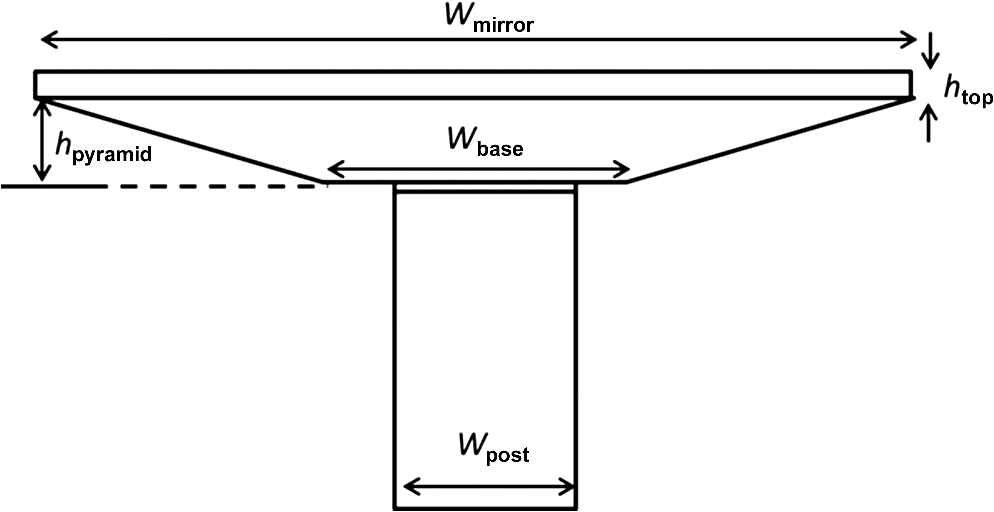
1.IntroductionMicromirrors and micromirror arrays have been an active area of microsystem device research for several decades. They remain so today, because they offer tremendous promise for enabling low-cost mass-producible systems for a variety of optical applications such as laser range sensing1 and phased array beamsteering.2 In many of these applications, it is ideal to have a micromirror that is both “optically flat” (i.e., possesses a large radius of curvature ), to prevent unwanted phase distortion and that enables a fast dynamic response. The dynamic response of the micromirror system is dependent upon both the subsystem dynamics of the particular actuation scheme employed and the mechanical frequency response of the entire structure. The latter can be a limiting factor for the entire system and is associated with the mode of operation intended for the mirror. For tip/tilt mirror systems that involve rotation about an axis, it is desirable to minimize the moment of inertia of the mirror to minimize response times. Likewise, for piston modes, uniformly minimizing the mass is desirable. The flatness of the mirror is limited by the internal stresses of the mirror structural layer and any coatings applied to it. Often, metallic coatings, usually Al or Au, which tend to have substantial thermal tensile stress from their deposition, are used to achieve the desired surface reflectivity for the intended optical system. For many years, micromirror designs were largely predicated upon surface micromachining methods using thin films.3,4 These designs tended to be very low mass/low moment of inertia, but exhibited unwanted curvature and nonuniformity in the mirror surface due to stresses inherent to the films and coatings used. Several clever approaches have been devised to minimize the unwanted deformation of these types of mirrors, including using vertical stiffening members,5 creating tensile membranes similar to a drum,6 and sandwiching lattice structures.7,8 The utilization of single-crystalline silicon to provide an inherently stiff flat mirror surface was proposed by some early bulk micromachined designs,9 but was not widespread until the emergence of silicon-on-insulator (SOI) fabrication technology in the late 1990, which offered readily available wafers with a thick releasable silicon device layer. The majority of micromirror designs since then have leveraged some form of an SOI MEMS process and most recognize the benefit of reducing the large mass associated with this approach. Designs that incorporate backside etching of the mirror surface have been presented for a variety of geometries and include hexagon patterns,10,11 truss structures,12 three-dimensional conical,13 and stepped14 approaches. As apparent from the work cited above, it has long been recognized that accommodating the structural rigidity of the mirror surface must be considered in conjunction with the system dynamic response during the structural design of the micromirror. Surprisingly, though, the authors of this work are unaware of anyone quantifiably reporting what the design tradespace looks like for a given design and how different mass reduction methods compare. In this work, using a raised square micromirror element as a baseline, we depict through modeling and simulation (COMSOL Multiphysics v5.2) how different mass reduction geometries, both original and suggested by literature, compare with mirror plate thinning alone in the curvature-mass tradespace. Mass was deliberately chosen as a metric over more direct measures of dynamic response, such as the system’s mechanical resonant frequency (i.e., the example shown in Sec. 2, Fig. 3) to portray the tradespace agnostic to any specific actuation scheme that may be employed. Furthermore, we successfully demonstrate that two-dimensional (2-D) patterns can be realized through a comparatively simple batch fabrication process that accommodates the presence of large features on the mirror backside. This is potentially useful for enabling mass reduction on SOI mirror geometries that use raised pedestals, such as Milanovic,12 to accommodate large tip/tilt angles. Finally, we suggest that the simulation approach utilized offers a sound means of tailored mass reduction design by direct comparison of measured and appropriately simulated radius of curvature values for select 2-D tessellated square mass reduction geometries. 2.Baseline Design Concept and CharacterizationThe square micromirror plate design () shown in Fig. 1 was chosen as the subject of this study. A central post in height and nominally square serves as a pedestal underneath the mirror, the bottom of which is intended to be bonded to an underlying actuation scheme (not shown). All solid models in this work assumed a fixed boundary condition at the base of the post. The mirror element is fabricated entirely from a single-sided SOI wafer with the process detailed in Sec. 5. Fig. 1Square baseline solid plate micromirror element (unpatterned): (a) side view and (b) solid model. 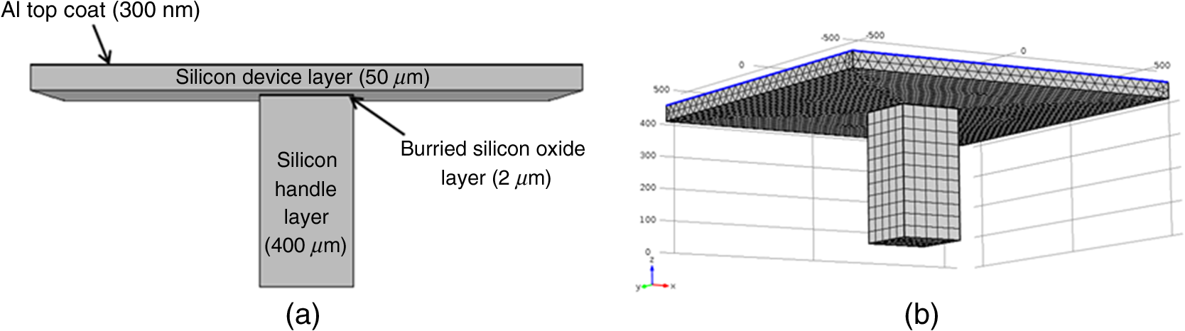 To clearly convey the impact element curvature has on optical performance, a simulation of the reflected optical far-field of an incident normal Gaussian beam on a mirror array with previously cited dimensions was created using methods covered by Schmidt.15 The simulation assumed a wavelength and 0.1 mm spacing between elements with an incident beam diameter equivalent to the lateral width of the array. Array elements were assumed to be perfectly uniform with zero tilt. Results for different radii of curvature are shown in Fig. 2 and clearly indicate that the reflected beam exhibits an increasingly segmented diffraction pattern as the radius of curvature decreases, with more power dispersed at larger off-axis angles. For most applications, the most uniform diffraction pattern is desired. Fig. 2.Far-field patterns of reflected Gaussian beam incident normal to the surface of the array: (a) , (b) , (c) , and (d) . 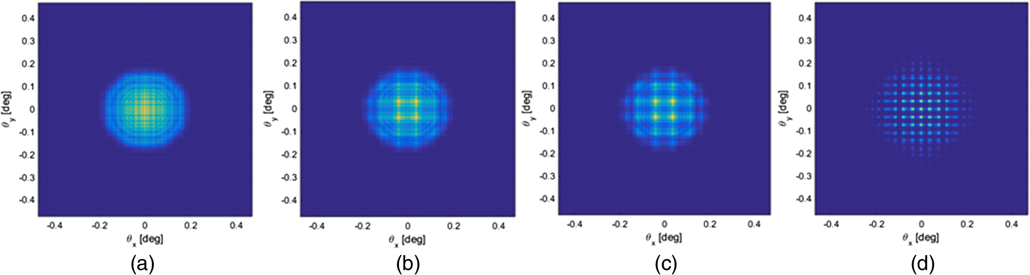 As previously explained, conveying the effect of mirror element mass on dynamic response in a quantitative sense requires the assumption of some notional undercarriage structure by which the element is supported and actuated. For this purpose, we utilized a simple low-deflection electrostatic cantilever structure made of polysilicon attached to the base of the mirror element to simulate via prestressed modal analysis how the resonant frequency of the modes of interest would change. The cantilevers were each coated in a stressed gold layer (300 MPa) to deform the cantilevers and effectively raise the entire element away from the substrate. Figure 3 specifically shows how the resonant frequencies of both the piston and tip/tilt modes, shown inset, change with mirror plate thickness. For comparison, an analytical estimation of how the piston mode resonant frequency would be expected to vary from the frequency, based on the equation where is the effective spring constant, is the effective mass, and is the thickness of the mirror in , is also provided and shows reasonable agreement with the simulation trend. As evident from the plots, the mechanical resonant frequency of the entire structure, which in many instances is the limiting factor in the overall system dynamics, can be increased significantly as the plate is thinned.Fig. 3Variation in mechanical frequency response for a solid plate micromirror system with a notional undercarriage.  Before conducting the study of different mass reduction backside pattern techniques, it was important to first anchor the simulations and analysis with biaxial film stresses that were experimentally representative. This characterization was begun by epoxy-bonding a small array of mirror elements onto a silicon wafer substrate and measuring the mirror surface deformation using interferometric microscopy (Zygo New View 7300). Figure 4(a) shows the array and the particular mirror elements used for the stress characterization. These samples differed from the depiction in Fig. 1 in that the buried oxide initially remained across the entire bottom surface of the mirror. The posts for these samples were and exhibited some misalignment off-center, but this had no impact on their usage for film characterization. Successive measurements were performed after the aluminum coating and this buried oxide layer were each individually removed (buried oxide remained in the position of the post). Deformation profile cuts of the data centered in the and directions were then tilt-corrected to allow direct comparison to similar cuts generated from mechanical simulation of each scenario in COMSOL. First, uncoated mirror data were used to compare to a parametric study of the stress in the silicon device layer. In this manner, the intrinsic stress in the device layer was determined to be to 30 MPa, and was chosen for the study. Second, the mirror data with the underlying buried oxide using this value of silicon stress were also compared with the parametric simulation of the oxide stress, as shown in Fig. 4(b). The buried oxide was determined to be in compression between and , and was the chosen value. In a similar fashion, the mirror data with both film layers were compared with appropriate simulations that varied the aluminum stress. The aluminum film stress was estimated to be 350 to 450 MPa in tension, and a film stress was utilized in the study. Once these film stress values were determined, analysis of different mass reduction approaches that could be applied to the mirror plate was conducted, beginning with the examination of plate thinning and its inherent limitations in the curvature-mass tradespace. Fig. 4(a) Stitched New View 7300 deformation data of the sample array with both aluminum coating and buried oxide layers present. Elements 2A and 3B are outlined in white. (b) Measured centerline deformation profiles of mirror elements (tilt corrected) with the Al coating removed and buried oxide remaining on back of mirror surface compared with steady-state deflection simulation results. 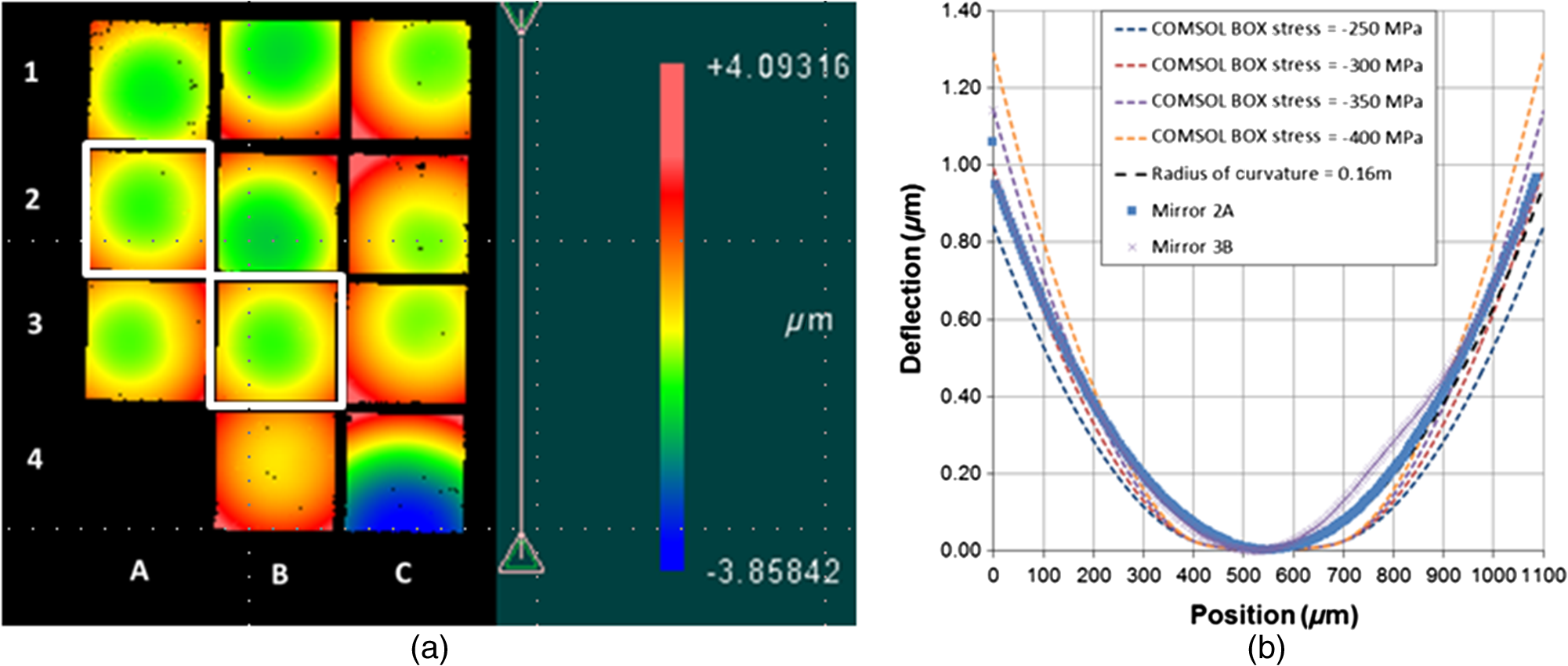 3.Solid Plate Thinning3.1.TheoryHow thin layered plates deform under thermomechanical loading has been the subject of significant study for many years and has been of particular interest to large surface area micromachined structures, including micromirrors. As explained by Dunn et al.,16 there are three deformation regions that a layered thin plate will experience as the film stress, which in the case of a metallic coating is dominated by thermal stress, increases in magnitude [Intrinsic (nonthermal) film and substrate stress is ignored in this formulation.]. The deformation regions are: (1) linear symmetric, where the applied stress is directly proportional to the resultant curvature and is symmetric about the center, (2) nonlinear symmetric, where the applied stress required to impart an increasing amount of curvature departs from the linear trend but remains symmetric about the center, and (3) nonlinear nonsymmetric, where the curvature in the lateral and vertical dimensions of the plate bifurcates, resulting in an elliptical curvature profile. Layered plate deformation that corresponds to the linear symmetric region is independent of plate size. A closed-form solution for the curvature in this region, assuming isotropic films characterized by a Young’s modulus , Poisson’s ratio , and thermal expansion coefficients , where refers to the surface film and the substrate, can be found to be where is the difference in coefficient of thermal expansion between the film and substrate , is the difference in temperature from the reference temperature at which the misfit strain between the film layers is zero, is the ratio of film thicknesses , and , where the biaxial moduli of each layer are (, 2). In the thin film limit , Eq. (2) can be approximated by performing a series expansion and retaining the lowest-order term, which yields the expression outside the brackets commonly referred to as the famous Stoney’s equation which is often experimentally applied to estimate stress in the surface film , particularly using silicon substrates.16,17 In this work, the difference between Eqs. (2) and (3) can be considered minor (see Fig. 6 for a direct comparison). Janssen et al.17 note that for silicon substrates, which are anisotropic, it is more accurate to utilize an appropriately defined biaxial modulus [e.g., for Si(100) , where and are the elements of the compliance tensor of silicon]; however, the difference is also insignificant for the scope of this work.Deformation in the symmetric nonlinear region does not have a simple closed-form solution and introduces dependence of curvature on plate size. As explained by Dunn et al.,16 this “behavior is due to geometric nonlinearity that results when the deflections become excessively large relative to the plate thickness and they contribute significantly to the in-plane strains.” An elliptical deformation profile coincident with region III deformation is undesirable for almost all optical applications of micromirrors; thus it becomes useful to know where this limit resides for a given geometry. Although calculating the deformation profiles associated with both nonlinear regions requires numerical methods, the critical curvature level at which the bifurcation occurs can be determined analytically, assuming isotropic films, using the equation 16 where , , and are the composite moduli for the entire composite film stack and are explicitly defined in textbooks.Throughout this work, a minimum thickness and feature resolution limit of was imposed as a practical measure to ensure the mass reduction patterns simulated, including plate thinning, could endure significant fabrication nonuniformity. All the mechanical simulations of mass reduction patterns for micromirrors presented in this work assume deformation that corresponds to the linear symmetric region, as did the simulations used to estimate film stress in Sec. 2. However, it was important to both validate and capture the limits of this assumption, and the thinned plate case is qualitatively the most stressing scenario. Thus, in addition to simulating the inherent limitations in the curvature-mass tradespace, additional emphasis was placed on the effects of nonlinearity for both regions II and III for plate thinning. 3.2.Simulation and AnalysisUsing COMSOL, a parametric sweep of the plate thickness from 5 to for steady-state linear plate deformation was performed accordingly for the baseline design shown in Fig. 1. Each film layer was assumed to be isotropic for the simulations, and the biaxial stresses as determined in Sec. 2 were applied. A summary of the material parameters used in the simulations throughout this work is given in Table 1. To estimate the resultant radius of curvature for the mirror surface, a least squares fit of the one-dimensional profile along the diagonal of the mirror was performed in Microsoft Excel using the procedure outlined by Brown18 to the spherical form where is the out-of-plane deformation in the axis and is the position along the diagonal. The mass of the plate was determined by both numerically integrating the density across the mirror plate and by analytical calculation (multiplying the density by the volume), which were verified as equivalent. Figure 5 depicts the resulting curvature-mass tradespace and compares it to estimates generated using Eq. (3). The agreement between the curves provides supportive evidence that the linear simulation was properly framed and conducted. Quantifying mass reduction patterns that are above and to the left of this curve is the subject of this work.Fig. 5Baseline simulated mass–curvature tradespace for mirror plate thinning (assumes linear deformation). The steady state z-displacement (scale ) for a mirror thickness of is shown inset. 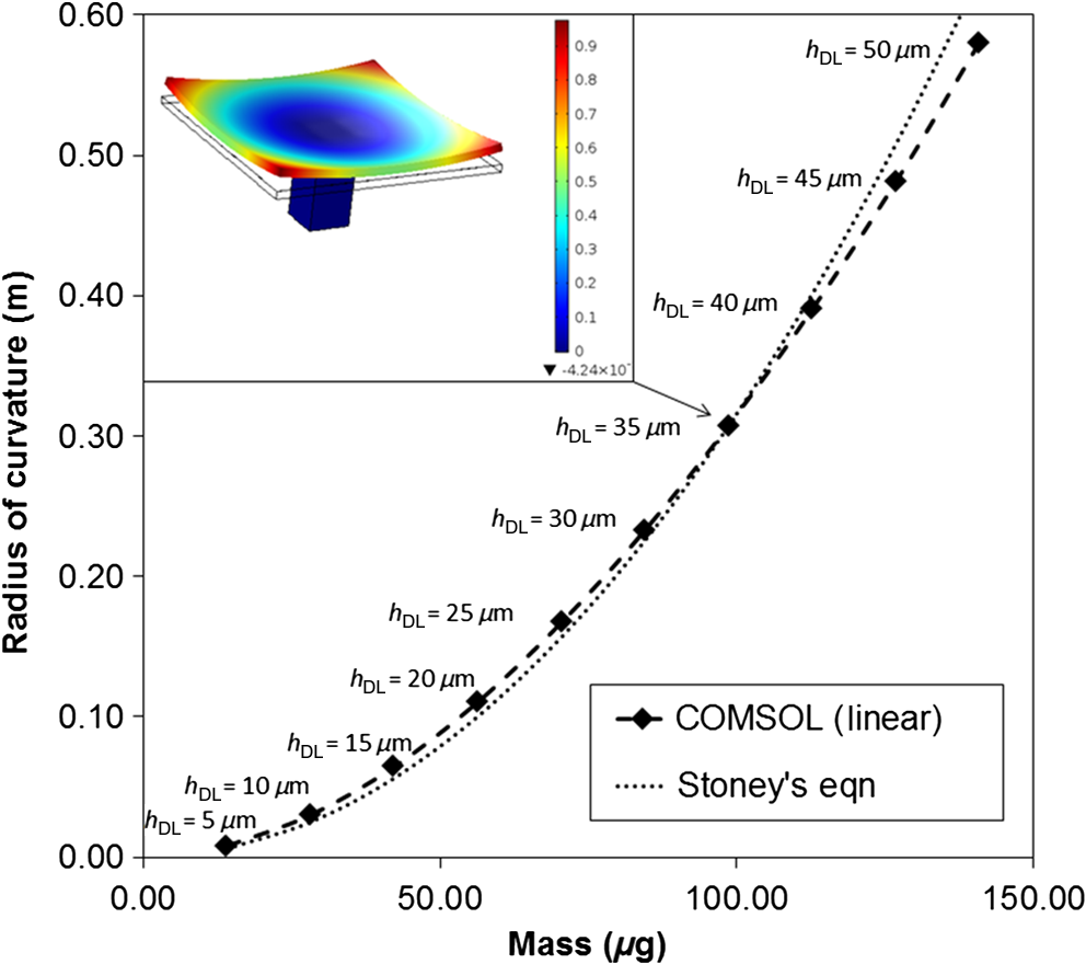 Table 1Summary of material parameters.
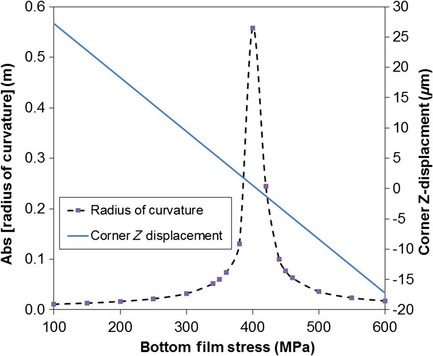
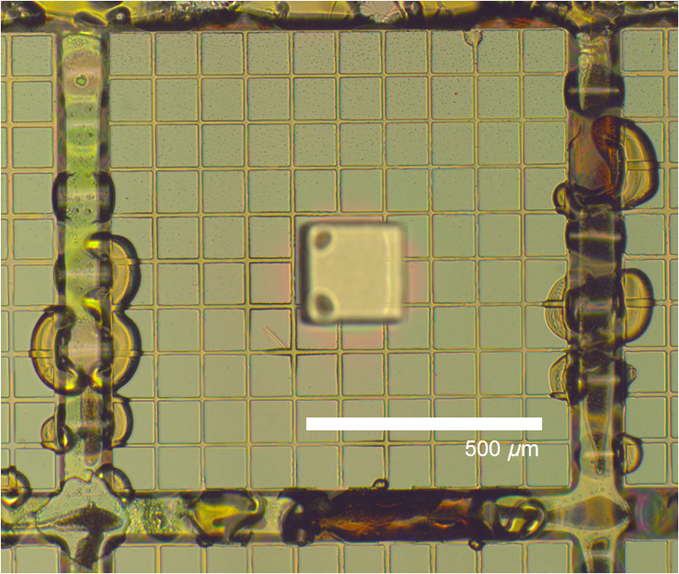
To verify that the presumption of linear deformation was reasonable throughout the mirror thickness range examined, additional steady-state mechanical simulations that incorporate geometric nonlinearity were performed in COMSOL. To explore the onset of the symmetric nonlinear region, region II, a corresponding parametric sweep with thickness was performed. By applying Eq. (4) for a square single crystal silicon plate with a 300-nm aluminum coating, the critical radius of curvature was also estimated. Figure 6 shows how the nonlinear and linear steady-state deformation simulations compare and at what thickness is reached. From Fig. 6, it is clear that region II onset begins below . However, because the values in this region are far from optically flat, the differences between the linear and nonlinear data through () can be considered minor for the micromirror application that is the subject of this work and support the assumption of linearity being sufficient for simulating the mass reduced geometries. Fig. 6Variation of the mirror plate radius of curvature with plate thinning using baseline parameters (Al film stress of ) and the critical bifurcation limit per Eq. (4). 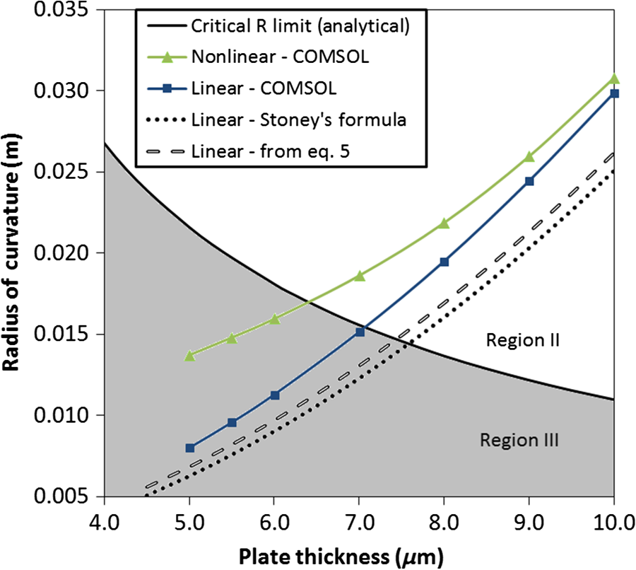 The intersection of the nonlinear profile with the critical radius of curvature limit shown in Fig. 6 suggests that region III deformation occurs at a thickness of with a critical of 0.0170 m (). To verify this transition point, a more direct simulation was performed with the intent of capturing transition of steady state deformation into region III. As explained by Dunn et al.,16 the bifurcation phenomenon is the result of natural asymmetries that occur in either geometry or material parameters. Thus, any numerical model must have some form of perturbation introduced to capture these effects in concert with the geometric nonlinearity. For this work, a geometric perturbation was introduced into the solid model of a -thick micromirror plate by making the surface slightly rectangular (). Geometric nonlinearity was again incorporated, and the aluminum film stress was parametrically swept from 300 to 475 MPa in 25-MPa increments to capture transition into region III with being fit across the lateral and vertical centerlines. Figure 7 shows the simulation results that suggest bifurcation occurring between 425 and 450 MPa with a curvature of at 425 MPa prior to bifurcation. This result appears reasonable in comparison to critical curvatures shown in Fig. 6, but suggests that the analytical critical limit yields a conservative result, because direct simulation required additional stress in the metal layer at the thinner mirror thickness for bifurcation to occur. Regardless, the simulation results support that the mass reduction geometries examined in this work, which incorporate a minimum plate thickness, are not at risk of region III deformation behavior. Fig. 7Simulated nonlinear deformation of a -thick micromirror with geometric perturbation: (a) variation of surface curvature with increasing aluminum film stress and corresponding surface deformation profiles for (b) 400 MPa, (c) 425 MPa, (d) 450 MPa, and (e) 475 MPa depicting region III bifurcation phenomenon. Scale shown is in micrometers. Dashed line in (a) indicates notional boundary between region II and region III deformation. 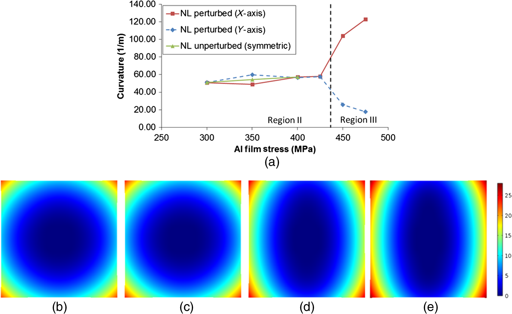 It is important to recognize that the plate thinning discussion to this point has been limited to single-sided film deposition. One alternative approach to mass reduction patterning is to deposit an additional equivalent metal layer to the backside of the plate to compensate the resulting stress in the plate and minimize deformation. This type of approach is theoretically valid but has a few significant drawbacks in regards to practical implementation. First, the micromirror design and fabrication would need to be made compatible with the additional metal deposition. This can be a challenge for designs that incorporate the mirror plate and support actuators in the same structural layer (e.g., Refs. 1 and 13), because additional lithography may be required to protect portions of the design where the metal would be detrimental. More significant, however, is that this stress-compensation approach demands strict tolerances in stress control of the film deposition. Figure 8 emphasizes this point by depicting the linear deformation results of a stress-compensated -thick micromirror plate generated from COMSOL simulation. For convenience, the radius of curvature for this particular plot was estimated directly in COMSOL using the following approximation of Eq. (5) where is the width of the micromirror and is the -displacement at the corner of the square plate. This approximation is valid for and offers insignificant differences (on the order of for a plate thickness from the least squares fitting of the diagonal approach used throughout this paper. As expected, optimal flatness occurs when the bottom film stress is equivalent to the top film, but the decreases precipitously with only of difference between the two layers. It is common for sputtered and evaporated metal films to exhibit both local stress variations and global variations between depositions in excess of this amount. Thus, achieving an optimal and uniform deformation result is often impractical with this approach.4.Mass Reduction PatternsIn this work, parametric studies for six different mass reduction patterns, some inspired by literature, were performed using COMSOL Multiphysics software to examine the displacement of the mirror surface and assess impact they have on the mass–curvature tradespace in comparison with the baseline micromirror geometry. Example solid models of each are shown in Fig. 9. Fig. 9Solid models of different mass reduced micromirrors examined: (a) hemispherical etch array (, , oblique view); (b,c) tessellated squares, bottom view (, ) and (, ); (d) ribbed truss design, bottom view (); (e,f) tessellated equilateral triangles, bottom view (, ) and (, ); (g) pyramidal frustum design (, ); and (h,i) tessellated hexagons, bottom view (, ) and (, ). 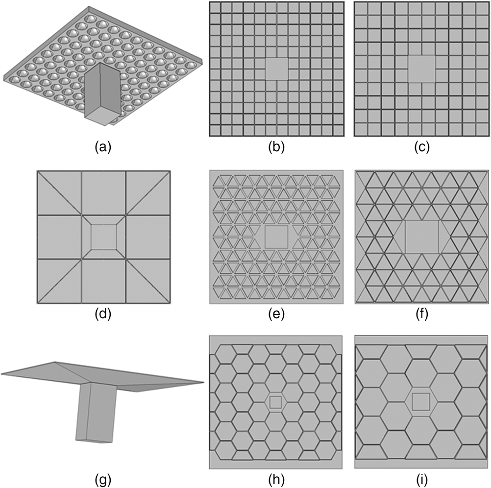 4.1.Hemispherical (Isotropic) Etch PatternsArguably the simplest mass reduction pattern examined was an array of hemispherical etches. This patterning was intended to be implemented by lithographically patterning an array of pinholes (5 to in size) into the oxide on the back of each element, which would then be etched isotropically using a reactive ion etch (RIE) or other chemical means [see Fig. 9(a)]. The radius of the hemispheres and the size of the square array were the two independent parameters for the model. Interhemisphere spacing was defined by The four center hemispherical array elements were reserved for the post structure and not removed. 4.2.Tessellated Shape (Square/Triangle/Hexagonal) Etch PatterningTessellated arrays of shapes were also considered as 2-D patterns for prismatic etching because they are simple to lay out. Though seemingly absent from the literature, tessellated squares, shown in Figs. 9(b) and 9(c), appeared desirable for this application because they conform to the symmetry of the square micromirror geometry. Hexagonal patterning, such as that used by Su et al.,10 and equilateral triangular patterning are inherently asymmetric patterns and thus will introduce some form of axial asymmetry in the curvature for this geometry. For completeness, implementations of these [see Figs. 9(e)–9(f) and 9(h)–9(i)] were nevertheless examined in part because of the prior work that suggested they may be desirable. The parameterization for each of these models used the shape sidelength dimensions (, , and , respectively), the etch depth and size of the tessellation array (the triangular and hexagonal used a single side as reference due to the asymmetry) as the dependent variables. Relations appropriate for each geometry, similar to Eq. (7), were then applied to space the tessellated elements evenly along the mirror length, with an equivalent spacing near the periphery of the mirror. Element spacing was given an artificially imposed lower resolution limit of to ensure high confidence in fabrication. In all cases, the area in the center of the tessellated pattern was reserved for the post (4 squares, 10 triangles, and a single center hexagonal element) based upon shape size. Thus, the lower tessellated patterns had reserved central areas that were in excess of the square size needed for the baseline geometry, making the higher patterns more favorable from a mass reduction standpoint. Tailored design of these excess areas near the post, as well as the unpatterned edge areas of the asymmetric tessellations, perhaps with a second-higher resolution tessellated pattern, is possible but was outside the scope of this work. 4.3.Ribbed Truss PatternA more traditional truss structure similar to that used by Milanovic et al.12 was also examined [see Fig. 9(d)] to provide a basis for comparison. This type of pattern is more aggressive in mass removal. The parametric studies for this geometry kept the post width fixed at and varied the truss width and depth . 4.4.Pyramidal FrustumThe final geometry examined in simulation was the pyramidal frustum. This geometry, shown in Fig. 9(g), is an extension of the conical backside geometry presented by Chui et al.13 but for a square instead of a circular micromirror. The patent from Moida14 shows a similar concept but in a graduated or stepped manner. This type of geometry is intended for laser-based optical systems that utilize a single micromirror rather than an array. However, the recent work with this approach made it interesting to explore and compare in the curvature-mass tradespace. In this case, the aim is to maximize the mirror flatness in the center of the mirror, where the majority of the incident Gaussian beam is impinging, while minimizing mirror mass at the periphery of the mirror to minimize the mirror’s moment of inertia and improve its rotational dynamic response. As presented by Chui et al.,13 fabrication of this geometry can be accomplished using a single backside mask and careful management of the deep reactive ion etch (DRIE) process. A cross-section of this geometry is provided in Fig. 10. For this work, a simple parametric sweep of was accomplished with and fixed at 5 and , respectively. 5.FabricationTessellated square mass reduction patterning was performed on two separate micromirror element array samples (arrays A and B) to both demonstrate the feasibility of the 2-D backside mass reduction patterning and validate the simulation results. A brief overview of the fabrication process on a single-sided SOI wafer is shown in Fig. 11. Fig. 11Brief outline of micromirror fabrication process incorporating 2-D mass reduction patterning using notional mirror element cross sections. 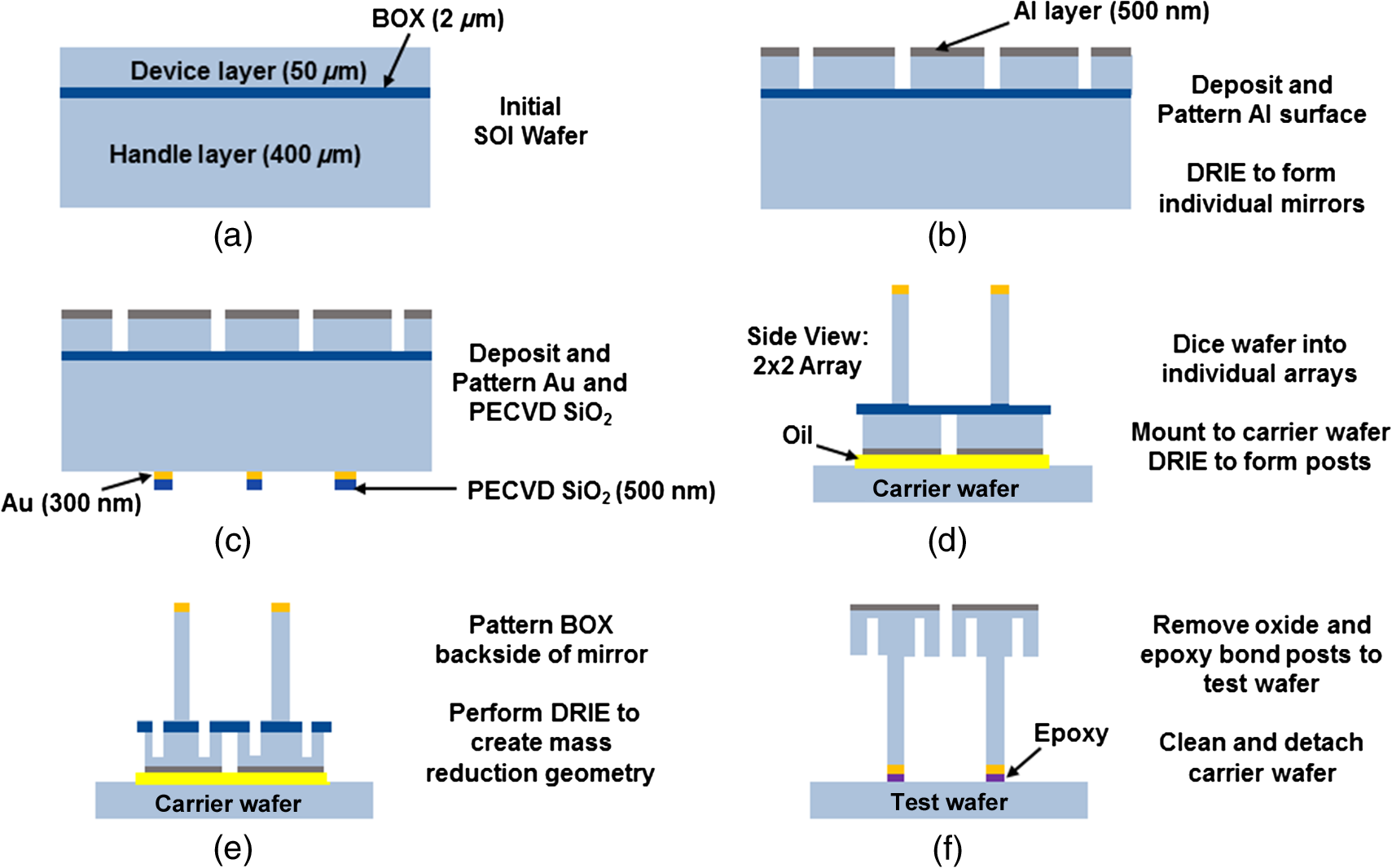 The process begins by patterning the desired metal layer on the device layer of the single-sided SOI wafer. The characterization samples used in Sec. 2 and simulated per Sec. 4 utilized a 30-nm Ti/300-nm Al surface coating. For the fabrication demonstration, samples with a thicker 450-nm Al coating and width of 1.0 mm were utilized; thus, the film stress was recharacterized in a similar manner as Sec. 2 using solid plate samples to allow direct comparison with simulation (see Sec. 6). This metal layer was then lithographically patterned to form the mirror element surfaces; serving both as a reflective coating and as a hard mask for subsequent selective DRIE to create the mirror plate. The central posts were then patterned on the handle layer surface in a similar fashion using a 30-nm Ti/500-nm Au/500-nm coating. The wafer was then diced into individual arrays, which were then individually mounted upside down onto handle wafers using thermally conducting oil as an adherent. Though not demonstrated, the post length can be reduced as desired by initial blanket thinning of the handle layer with RIE followed by chemical mechanical polishing. Once the post pattern is complete, a second DRIE etch of the handle layer to the buried oxide (BOX) was performed to form the posts. The mirror array is held together at this point by the interconnecting BOX layer and the oil interfacing with the carrier wafer [see Fig. 11(d)]. To keep the oxide wet etch times reasonable, the BOX layer was further thinned by to 1000 nm using a blanket RIE etch (Plasmatherm 790, 40 sccm , 3 sccm , 40 mTorr, 200 W). To accommodate the -high posts, the patterning of the mass reduction pattern on the backside of the micromirror was accomplished using projection lithography. This pattern was transferred to the BOX layer by a timed wet etch ( buffered oxide etch, 12 min 30 sec at room temperature) and subsequently etched into the silicon using a third timed DRIE etch. All three DRIE etches in the process use a common 3-step time-multiplexed recipe (PlasmaTherm Versaline VL-8526 with and chemistries). The arrays were then cleaned in acetone, and the BOX layer was removed using a final wet etch. For functional micromirror devices, the mirror element posts would be epoxy-bonded to an actuation undercarriage for device assembly. In this work, it was sufficient to bond the elements (FineTech Fineplacer femto) to a second test wafer because only the resultant surface curvature profiles were of interest. A final cleansing of the arrays was performed by solvent rinse, which is compatible with the epoxy bond. Overall, this process is unique in its ability to accommodate large free-standing features and advantageous in its simplicity when compared to other mass-reduction methods because it employs a single mask and DRIE etch step to perform the mass reduction across the array. As a point of comparison, the process presented by Milonovic et. al.,12 which enables multitiered thicknesses, requires three separate lithography and etch steps. Although the process used was largely successful and sufficient for the purposes of this demonstration, additional maturation would be required before extending it to an actual product line because a few challenges with it were experienced. The most significant challenge is that these samples utilized an Al coating, which is incompatible with HF or BOE wet etchant. To address this, the final BOX removal was performed before bonding to allow the conductive oil to protect the surface of the mirror. Because the adhesion of the mirror elements to the oil is inherently imperfect, and the oxide itself is very fragile, several elements in the arrays detached during the penultimate wet oxide removal processing step. In addition, examination of the mirror surface after the final bonding step showed all the mirror coatings on array B were severely damaged, and several in array A had significant imperfections. This issue is most easily addressed by removing the interconnecting BOX after bonding the array and either utilizing a HF compatible coating, such as Au, or by using an oxide etchant that is compatible with Al, such as the glycerine-buffered HF mixture reported by Gajda.19 Further, several array elements exhibited some imperfections in lithography, particularly near adjacent elements due to beading of resist near the element interfaces (see Fig. 12). This is in part due to deformation of the interconnecting oxide layer impeding a smooth distribution of resist during spin application. Additional refinement of spin-based resist application and or a resist spray approach would likely resolve these imperfections. Two tessellated square mask reduction patterns, , of different resolutions () and () were applied to each array in a checkerboard arrangement. Several manual measurements on optical images of the resulting geometry patterns prior to bonding were performed on elements of each array, with the average measured being 88.9 and for each pattern, respectively. These patterns offered central squared masked areas with widths of 208.7 and , making them compatible with the post. The resolution lost during processing matched expectations of the wet BOX etch. Surface profilometry and interferometric microscopy [see Fig. 13(c)] were also performed prior to BOX removal to capture the pattern depth and surface texture post etching. Interestingly, the etches of each array sample were very different in result, with one sample being much rougher in texture than the other [see Figs. 13(a) and 13(b)]. This was attributed to a very thin lingering oxide layer inhibiting the etch of one of the array samples (array A) and causing micromasking effects. Although the underlying surface texture is not impactful from a structural perspective, assuring full removal of surface oxide is important for consistent process control. The measured etch depths () were for array A and 35 μm for array B. Fig. 13Micromirror element backside images with fabricated tessellated square mass reduction patterns. SEM images: (a) of an array B element with underside surface roughening and (b) an array A element that exhibits cleaner etching with some micropillars. An example full-surface profile of a micromirror element backside captured from a white light interferometry system is shown in (c). All images were collected prior to removal of the buried oxide. 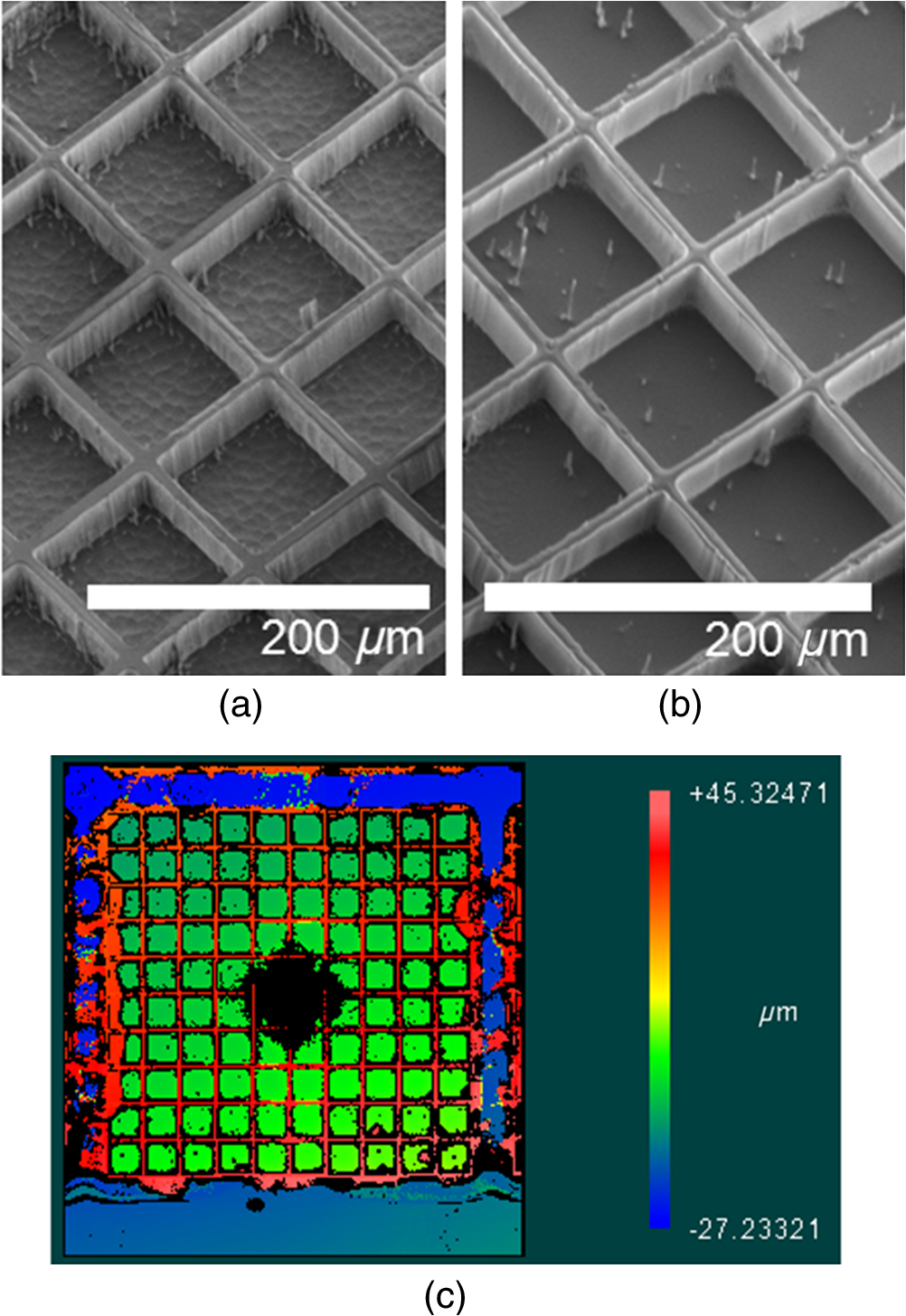 6.Results and DiscussionThe static deformations of the geometries discussed in Sec. 4 were each examined in simulation with the same 300-nm Al top coating and material stresses as previously mentioned. It is important to note that an exhaustive examination of all possible geometric parameters was not conducted for each mass reduction pattern, but rather selected sweeps were conducted that gave a sense of the limits each parameter had in the tradespace. Figure 14(a) plots how these geometry sweeps compared to the solid plate baseline. Similar to the solid plate thinning discussed in Sec. 3, the mass of the post was not included in this comparison. Analytical calculations for mirror mass were confirmed to match those generated in COMSOL in all instances. Fig. 14(a) Simulated results for each micromirror mass reduction pattern as mapped to the mass–curvature tradespace (, Al film coating 300 nm thick with internal stress). Select geometry dimensions of interest are labeled. (b) Specific parametric sweeps of etch depth for 2-D truss (), tessellated square (, ), tessellated triangles (, ), and tessellated hexagons (, ) mass reduction patterns in comparison to the thickness removed for a solid plate. 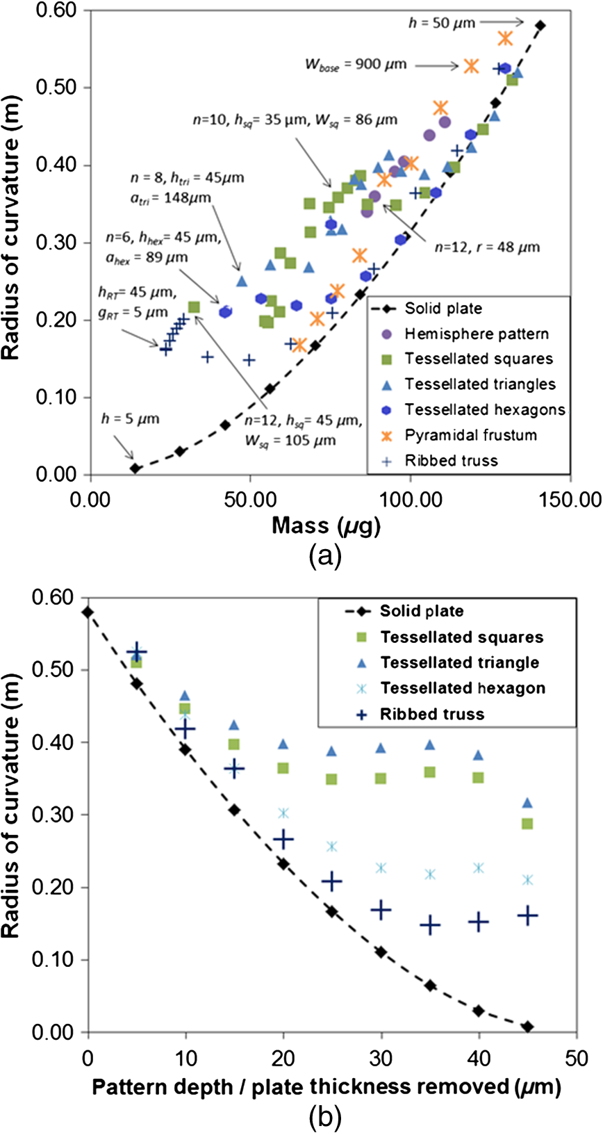 There are several takeaways from these results. First, it is clear from Fig. 14(a) that significant improvements () in radius of curvature for a given mass point are attainable using mass reduction methods. Second, mass reduction patterning is not universally beneficial in comparison with simple solid plate thinning. This becomes most apparent in the case of the etched 2-D backside patterns (truss and tessellated patterns), where plotting of parametric sweeps of etch depth show design points largely coincident with the solid plate for a portion of the sweep. Figure 14(b) shows this more clearly by directly comparing these sweeps sans the other design points plotted in Fig. 14(a). This tendency makes intuitive sense because these specific structures are essentially solid plates with underlying support structures, and significant departure from solid plate behavior is not expected until the proportion of support structure to the plate is substantial. In addition, Fig. 14(a) shows that the more aggressive the 2-D etch area, with the truss design being the most aggressive and tessellated triangles being the least, the deeper the etch must be to provide benefit. For instance, the truss structure does not provide benefit compared with the solid plate until more than of etch depth have been reached. It is reasonable to presume from these trends that the etch depth point of departure from solid plate can be tailored to most values within these bounds by designing the etch pattern appropriately. The pyramidal frustrum and hemispherical etch array, which leverage nonuniform etching with depth, follow alternate trends with geometry variation that afford benefit from the solid plate in the higher mass portion of the tradespace. Though the curvature-mass tradespace is the primary tool for comparison in this work, it is inherently an aggregate metric. Considerations of the surface profile and smoothness (and symmetry, as previously mentioned) may also be important for optical performance, especially in instances of aggressive mass reduction. For example, the diagonal deflection profiles in Fig. 15 show how the pyramidal frustrum geometry indeed exhibits less curvature in the center of the mirror and more at the edges as expected, making the fit to Eq. (5) less representative of the actual profile. The deformation of the truss geometry for , shown in Fig. 16(a), indicates that subtle rippling in the deformation can result, which induces unwanted aberrations into the optical system. Figure 16(b) shows that a case for a tessellated square micromirror geometry does not exhibit this effect. Fig. 15Plot of steady-state -axis deformation along the half-diagonal of pyramidal frustrum geometry for varying values ( fixed at ). Inset is a surface plot of the -axis deformation viewed from below the micromirror for the condition. The white dashed line shows the half-diagonal portion plotted. 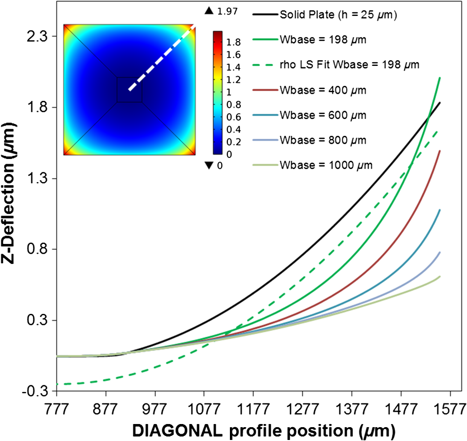 Fig. 16Surface plots of steady-state -axis deformation for (a) a truss geometry , and (b) a tessellated square pattern , , micromirror elements. 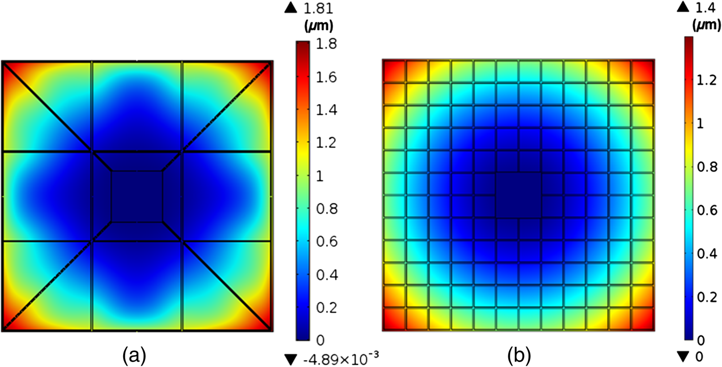 The stress characterization study performed on the solid plate samples () with the 450-nm Al layer found the tensile film stress to be significantly lower, at approximately 80 to 100 MPa, than the previously characterized 300-nm sample shown in Sec. 2, on which Fig. 14 is based. Although the exact cause of the difference in the Al film stress between samples is unclear, conceptually the mass–curvature tradespace can be portrayed in the same manner as previously shown. Simulation for the surface deformation was performed in COMSOL using a 100-MPa stress value for the appropriate mass reduction geometries to allow a direct comparison with select array A mirror element measurements where the optical coatings were sufficiently intact, as shown in Table 2. In addition, simulation of comparable mass solid plate elements is shown to quantify the curvature benefit in this specific region of the tradespace. Both measured and simulated values were determined by least squares fitting to the diagonal deformation profile, as described in Sec. 3.2. Figure 17 shows how the measured values in Table 2 compare graphically in the appropriate tradespace, assuming the samples have mass as calculated. Fig. 17Simulated and measured results listed in Table 2 shown on appropriate mass–curvature tradespace (, Al film coating 450 nm thick with internal stress). 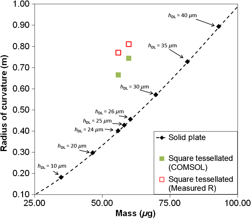 Table 2Summary of micromirror element curvature measurements (Wmirror=1.0 mm, Al film coating 450 nm thick with +100 MPa internal stress).
Overall, the measured and simulated values agree reasonably well, although the simulation tends to yield values of slightly greater curvature than observed in measurements. These differences may be an artifact of coating thickness and stress variations between the elements and differences in the deformation profile near the post, largely due to the boundary condition imposed in the simulation. The comparison with solid plate elements of similar mass shows modest improvements in , as expected. 7.ConclusionsOverall, this work demonstrates that examining mass reduction of micromirrors from a curvature-mass tradespace perspective is valuable, and arguably necessary, to quantify the benefit of different 2-D mass reduction geometries. Patterning of a 2-D tessellated square pattern was successfully demonstrated in the presence of large free-standing structures with sufficient results to show that simple 2-D patterning can be accomplished with minimal additional lithography and processing. The example geometries chosen for the samples processed indicated improvement in radius of curvature compared to a solid plate of equivalent mass based on simulations validated with experimental data. The use of finite element models that assume geometric linearity has been shown to be effective for simulating reasonable predictions of curvature for these types of geometries. Specific geometric optimization of the 2-D mass reduction patterns for specific regions of the tradespace was not conducted in this work, and may yield results that further improve upon what is presented. AcknowledgmentsThe authors wish to acknowledge the efforts of AFRL laboratory technician Mr. Andrew Browning for performing silicon etching for samples presented in this work. The authors would also like to acknowledge Dr. Dave Van Veldhuizen and Dr. John Cetnar for helpful technical discussions and guidance. ReferencesU. Hoffman et al.,
“Resonant biaxial 7-mm MEMS mirror for omnidirectional scanning,”
J. Micro/Nanolithogr. MEMS MOEMS, 31
(1), 011103
(2014). http://dx.doi.org/10.1117/1.JMM.13.1.011103 Google Scholar
T. K. Chan et al.,
“Optical beamsteering using an MEMS phased array with closed-loop interferometric phase control,”
Opt. Express, 21
(3), 2807
(2013). http://dx.doi.org/10.1364/OE.21.002807 OPEXFF 1094-4087 Google Scholar
P. M. Hagelin and O. Solgaard,
“Optical raster-scanning displays based on surface micromachined polysilicon mirrors,”
IEEE J. Sel. Top. Quantum Electron., 5
(1), 67
–74
(1999). http://dx.doi.org/10.1109/2944.748107 IJSQEN 1077-260X Google Scholar
W. Cowan et al.,
“Design and testing of polysilicon surface-micromachined piston micromirror arrays,”
Proc. SPIE, 3292 60
–70
(1998). http://dx.doi.org/10.1117/12.305508 PSISDG 0277-786X Google Scholar
B. J. Lutzenberger and D. L. Dickensheets,
“Vertical stiffening members for flatness control of surface micromachined structures,”
Proc. SPIE, 4561 238
–246
(2001). http://dx.doi.org/10.1117/12.443091 PSISDG 0277-786X Google Scholar
J. T. Nee et al.,
“Stretched-film micromirrors for improved optical flatness,”
in IEEE 13th Annual Conf. of Micro Electro Mechanical Systems (MEMS 2000),
704
–709
(2000). http://dx.doi.org/10.1109/MEMSYS.2000.838604 Google Scholar
S. Kurth et al.,
“Silicon mirrors and micromirror arrays for spatial laser beam modulation,”
Sens. Actuators A, A66 76
–82
(1998). http://dx.doi.org/10.1016/S0924-4247(97)01731-7 SAAPEB 0924-4247 Google Scholar
G.-D. Su, P. Patterson and M. Wu,
“Surface-micromachined 2D optical scanners with optically flat single-crystalline silicon micromirrors,”
Proc. SPIE, 4293 46
(2001). http://dx.doi.org/10.1117/12.426942 Google Scholar
C.-H. Ji et al.,
“An electrostatic scanning micromirror with diaphragm mirror plate and diamond shaped reinforcement frame,”
J. Micromech. Microeng., 16 1033
–1039
(2006). http://dx.doi.org/10.1088/0960-1317/16/5/021 JMMIEZ 0960-1317 Google Scholar
V. Milanovic, G. Matus and D. McCormick,
“Gimbal-less monolithic silicon actuators for tip-tilt-piston micromirror applications,”
IEEE J. Sel. Top. Quantum Electron., 10
(3), 462
–471
(2004). http://dx.doi.org/10.1109/JSTQE.2004.829205 IJSQEN 1077-260X Google Scholar
B. W. Chui et al.,
“Simplified monolithic process for fabricating low-cost, high frequency, high flatness scanning micromirrors,”
in Solid-State Sensors, Actuators, and Microsystems (TRANSDUCERS 2013),
1036
–1039
(2013). http://dx.doi.org/10.1109/transducers.2013.66.26947 Google Scholar
J. D. Schmidt, Numerical Simulation of Optical Wave Propagation with Examples in MATLAB, SPIE Press, Bellingham, Washington
(2010). Google Scholar
M. L. Dunn, Y. Zhang and V. M. Bright,
“Deformable and structural stability of layered plate microstructures subjected to thermal loading,”
J. Microelectromech. Syst., 11
(4), 372
–384
(2002). http://dx.doi.org/10.1109/JMEMS.2002.800932 JMIYET 1057-7157 Google Scholar
G. C. A. M. Janssen et al.,
“Celebrating the 100th anniversary of the Stoney equation for film stress: developments from polycrystalline steel strips to single crystal silicon wafers,”
Thin Solid Films, 517 1858
–1867
(2009). http://dx.doi.org/10.1016/j.tsf.2008.07.014 THSFAP 0040-6090 Google Scholar
A. M. Brown,
“A step-by-step guide to non-linear regression analysis of experimental data using Microsoft Excel,”
Comput. Methods Programs Biomed., 65 191
–200
(2001). http://dx.doi.org/10.1016/S0169-2607(00)00124-3 CMPBEK 0169-2607 Google Scholar
J. J. Gajda,
“Techniques in failure analysis of MOS devices,”
in 12th Annual Reliability Physics Symp.,
30
–37
(1974). http://dx.doi.org/10.1109/IRPS.1974.362623 Google Scholar
BiographyHarris J. Hall is a senior research electronics engineer at the Air Force Research Laboratory. He received his BS degree in electrical engineering from Rensselaer Polytechnic Institute in 1999, his MS degree in electrical engineering from the Air Force Institute of Technology (AFIT) in 2001, and his PhD in mechanical engineering from the University of Colorado Boulder in 2013. His current research interests include micro/nanoscale resonant systems and micromirrors. Andrew Green joined the Air Force Research Laboratory in 2014 where he researches ZnO, GaN, and device technologies. He received his BS and PhD degrees in chemistry from Ohio University in Athens, Ohio, in 2010 and 2013, respectively. Sarah Dooley is an electronics engineer at the Air Force Research Laboratory, where she works in the field of nonmechanical beam steering, including the design, fabrication, and characterization of micromirror arrays. She also collaborates with several institutions on the development of plasmonic and liquid crystal beam-steering techniques, MEMS optical switches, and MEMS frequency generation technology. She received her BS degree in physics from Xavier University in 2002 and her MS in electro-optics engineering from the University of Dayton in 2004. Jason D. Schmidt is a senior scientist at MZA Associates Corp. and a US Air Force Reserve officer at the Air Force Research Laboratory. He received his BS degree in physics from Marquette University in 1998, his MS degree in physics from The Ohio State University in 2000, and his PhD in electro-optics from the University of Dayton in 2006. He has 15 years of experience in electro-optics, imaging, atmospheric and adaptive optics, wave-optics simulation, directed energy, aero-optics, free-space optical communication, and laser radar. LaVern A. Starman is a principal electronics device engineer at the Air Force Research Laboratory and adjunct faculty at Wright State University. He received his BS degree from the University of Nebraska, Lincoln, in 1995, his MS degree from Wright State University in 1997, and his PhD from the AFIT in 2002, all in electrical engineering. His current research focus areas are material stress characterization, optical beamsteering, and MEMS-based sensors and actuators. Derrick Langley is a US Air Force officer currently stationed at Advanced Systems and Development Directorate, Space and Missile Systems Center (SMC), Los Angeles AFB, California. He received his BS degree in electrical engineering from the University of Central Florida in 2003, his MS degree in electrical engineering from Wright State University in 2007, and his PhD in electrical engineering from the AFIT in 2012. Prior to his assignment at SMC, he was an assistant professor at AFIT teaching courses in microelectronics, MEMS, and nanotechnology. Ronald A. Coutu, Jr., is an associate professor of electrical engineering and cleanroom director at the AFIT at WPAFB, Ohio. He received his BS degree from the University of Massachusetts at Amherst in 1993, his MS degree from California Polytechnic State University in San Luis Obispo in 1995, and his PhD from AFIT in 2004, all in electrical engineering. His current research interests include MEMS, smart sensors, microelectrical contacts, and phase-change materials. |