
|
|
1.IntroductionCritical dimension atomic force microscopes (CD-AFMs) were developed in the early 1990s1 and are now a significant presence in semiconductor manufacturing metrology. CD-AFMs utilize flared tips coupled with two axes of tip control to enable imaging of near-vertical sidewalls. There are many potential contributors to the uncertainty of CD-AFM measurements, but these generally fall into two broad categories: scanner calibration and motion errors and tip-related effects. Since the scanner-related sources of uncertainty can normally be limited to ∼0.1% of the measured feature size, the uncertainty in most CD-AFM width measurements, particularly below the 500-nm level, is dominated by tip-related errors. The interaction of a CD-AFM tip and a sample surface is complex and three-dimensional. While it consists largely of geometrical effects,2,3 there are also attractive forces and the potential for nongeometrical effects due to tip bending.4 Despite this complexity, many imaging effects can be understood using a two-dimensional model. In this simplified picture, the effect of the tip is represented as a constant additive offset that must be subtracted from the apparent width to obtain an accurate measurement. This approach to tip correction for CD-AFM linewidth metrology has been described as a “single measurand method.” All of the detailed analyses to extract a linewidth value are initially performed on the raw data, and, subsequently, a scalar offset is applied to correct the measured width.5,6 This contrasts with more complex approaches based on mathematical morphology and slope matching.2,3,7,8 For purposes of tool calibration and monitoring, the accuracy of the CD-AFM tip width calibration depends on a reference structure of known width that is stable over time and with repeated measurements. Since 2004, there have been standards for CD-AFM tip calibration available both commercially9 and through the National Metrology Institutes (NMIs), such as the National Institute of Standards and Technology (NIST) in the United States5,10 and more recently the Physikalisch-Technische Bundesanstalt (PTB) in Germany.11,12 The accuracy of these standards has been validated by interlaboratory comparisons. However, less attention has been paid to long-term stability, which could be important for tool monitoring. In principle, only a single standard is required to calibrate CD-AFM tip width. However, with any measurement process and even in the most favorable environmental conditions, there is always a possibility that a sample may be affected by wear or contamination or otherwise deteriorate from its original condition. It is thus advantageous to cross-check using multiple standards in some manner. A common practice in manufacturing metrology is to regularly measure a “golden” product wafer as a tool monitor subsequent to the tip calibration.13 This approach would readily detect changes in either the tip calibration standard or the monitor wafer, except for the improbable case of common-mode deterioration in both. The availability of additional cross-check data may also be useful if the calibration standard has to be cleaned since any unintended change or damage due to the cleaning process will be apparent. While the need for cleaning standards should be infrequent with proper storage and handling, it is a possibility that should be generally anticipated. Following the initial development of the NIST standard, which is known as the single-crystal critical dimension reference material (SCCDRM), we compared the SCCDRM calibration with a subsequently developed commercial standard.14 The physical principles used to calibrate the SCCDRM and the commercial standard were similar. Both were based on the use of a high-resolution transmission electron microscope (HRTEM) and resolution of the silicon lattice spacing for width calibration. However, these implementations were entirely independent. In our earlier paper on this comparison, we demonstrated agreement of these two calibrations.14 In this paper, we update these results by demonstrating the long-term stability of these samples and subsequent comparisons between them. Although there were circumstances in which these samples needed to be cleaned, our results show agreement within the uncertainties and stability over a period exceeding 10 years. Due to the extended period in which this work took place, it involves three different CD-AFM instruments. The use of these instruments is a reflection of the tools we had available at the time of each measurement and does not mean that more than one instrument is necessary for sample monitoring. However, this does highlight a potential benefit of long-term sample monitoring: When one tool is being replaced with another one, it is helpful to have the confidence in the calibration samples that can be established through long-term monitoring. If a sample was degrading over time, this could complicate the linking of successive instruments. In our case, the use of multiple standards provided a crucial link between measurements performed using different instruments over a considerable period of time. 2.Experiment: Instruments, Uncertainty, Samples, and Measurements2.1.Critical Dimension Atomic Force Microscope Instruments and UncertaintyThree CD-AFM instruments were involved in this work: a first-, second-, and third-generation CD-AFM. At the ground level of detail, there are differences among these systems with respect to design architecture, detection methods, software interface, the degree of automation, and the types of tips that the scan control can accommodate. For example, first-generation systems used interferometry to detect cantilever deflection, while subsequent generations employed the more common optical lever method. These differences are generally reflective of the measurement needs and the state of technology at the time the systems were introduced. In terms of function, however, most of these differences represent logistical constraints rather than limitations on measurement performance or ultimate accuracy. One noteworthy exception to this is tip size accommodation in the scan control. The tip position and scan control on third-generation systems are generally more stable and better able to accommodate very small tips. Third-generation systems can reliably scan using tips as small as 15 nm. First-generation systems typically functioned best using tips larger than 100 nm and were generally unable to make effective use of tips smaller than 70 nm. Tip wear also tends to be a greater challenge in first-generation systems. However, with all CD-AFMs, the observed tip wear depends greatly on the geometrical and material characteristics of both the tip and the measured feature. Ultimately, however, despite some noteworthy differences in implementation and the range of applicability among the different generations of CD-AFM tools, the resulting measurement capability of all CD-AFMs is both conceptually and functionally equivalent, provided that a given tool is operating within its range of applicability. This fact will be underscored by our results. For purposes of this paper, we refer to the three different instruments used as CD-AFM1, CD-AFM2, and CD-AFM3. Note that these labels were chosen such that the numerical component also corresponds to the generation of the instrument. CD-AFM1 and CD-AFM3 are located in our laboratories at NIST, although CD-AFM1 has now been decommissioned. CD-AFM2 was housed at SEMATECH, and measurements were performed with it as part of a major collaboration between the organizations. All three of these instruments were calibrated and characterized by NIST, so traceable measurements could be performed.15–17 To describe measurement and calibration uncertainties, NIST and most other NMIs follow the approach to uncertainty budgets that is recommended by the International Organization for Standardization.18,19 This involves developing an estimated contribution for every known source of uncertainty in a given measurement and includes terms pertaining to both the instrument used and the particular specimen measured. Terms evaluated exclusively by statistical methods are known as type A evaluations. Other terms, known as type B evaluations, are evaluated using some combination of measured data, physical models, or assumptions about the probability distribution. All of these terms are then added in quadrature to obtain a combined standard uncertainty for the measurement. This is usually multiplied by a coverage factor to obtain a combined expanded uncertainty. The most common coverage factor used is , which would correspond to confidence for a normal (Gaussian) distribution. Uncertainty budget templates for pitch, height, and width measurements were developed for CD-AFM1,15 CD-AFM2,16 and CD-AFM3.17 The tip width on all three CD-AFM instruments was first calibrated using the NIST tip width calibration standard, and then this calibration was used to measure the widths of the independently developed commercial standards. The detailed characteristics of these samples and the measurements are discussed in the following sections. 2.2.Tip Width Calibration StandardsThe NIST standard for CD-AFM tip width calibration is known as SCCDRM. NIST, SEMATECH, and VLSI Standards collaborated on the development and release of SCCDRMs to SEMATECH member companies in 2004.5,10 The SCCDRM features have near-vertical sidewalls, accomplished using preferential etching on {110} silicon-on-insulator substrates.5,10 The structures included linewidths as low as 50 nm and ranging up to 240 nm and having expanded uncertainties () of typically 1.5 to 2.0 nm. However, the SCCDRM master standard at NIST allows width measurement uncertainties as low as 0.6 nm (). Traceability to the SI (Système International d’Unités or International System of Units) meter was accomplished through the use of HRTEM, which enables counting the number of silicon lattice planes in the calibration sample. Although the HRTEM measurement process is destructive, prior CD-AFM comparator measurements made it possible to transfer the calibration to remaining samples. At about the same time as the SCCDRMs were developed, a commercial product of similar applicability was introduced.9 For purposes of this paper, we will refer to these samples as commercial critical dimension standards (CCDSs). These specimens are fabricated using a technique that involves deposition of alternating layers of silicon and oxide, followed by a cross section and oxide etch.9 The CCDS samples are available in nominal widths of 25, 45, 70, and 110 nm. The uncertainties were assessed independently using measurements performed on each lot. Generally, the expanded uncertainties () are estimated to be for most samples. The traceability of the CCDS calibration is also derived through the use of HRTEM, although the implementation is different from the SCCDRM method. The actual target features of the CCDS samples are poly-crystalline, so the feature width cannot be directly calibrated by lattice plane counting in a transmission electron microscope (TEM) image. However, the design of the CCDS is such that there is a crystalline structure adjacent to the target features. Lattice-resolving HRTEM can be applied to this structure and used to calibrate the scale of an image, which contains the actual poly-crystalline target feature. The SCCDRMs and the CCDSs were fabricated using different technology and were calibrated independently. The overall goals of this work were to compare the agreement between these two independent TEM-based calibrations of width across multiple CD-AFM platforms and to evaluate the long-term stability of all the standards involved. For purposes of the comparison presented in this paper, we selected the 45- and 70-nm samples, which we refer to as the CCDS45 and CCDS70, and measured these samples using the SCCDRM tip width calibration procedure. Although the fundamental principles involved in the calibration and use of the SCCDRM and CCDS are similar, there are relevant differences in design and layout. The SCCDRM is optimized for navigation in which a measurement window can be readily positioned to overlap with the location of a prior measurement. This is accomplished through the unique target identification number and the navigation markers on each target. This is important for actual use in CD-AFM tip calibration, and it was also crucial to the AFM-to-TEM transfer stage of the original SCCDRM calibration. In that experiment, it was necessary to compare HRTEM and CD-AFM measurements taken at the same locations on the same features. Navigation markers were useful for ensuring the measurement window overlap. The CCDS samples are also equipped with navigation aids. However, in contrast to the SCCDRMs, these samples are optimized for global uniformity over the entire 3-mm length of the available feature. This long-range uniformity is a consequence of the film deposition techniques used in the manufacture of the standard.9 The navigation markers on the CCDS samples facilitate remeasuring the same location. This can improve the apparent reproducibility of the measurement, since different locations do exhibit small differences. However, the measurand definition specified for the CCDS provides a global reference value and uncertainty, which is intended to be applicable anywhere on the specimen, and the navigation markers do not play a role in this definition. Additionally, the SCCDRM and CCDS samples are significantly different in form factor. The SCCDRMs are in the form of silicon chips, each , that were diced from a 150-mm wafer. The CCDS samples are in the form of a much smaller chip, , that were cut in a cross section from the wafer. Due to this smaller size, the CCDS samples are more difficult to handle, so they are available from the vendor premounted inside a larger silicon chip, , which is sometimes referred to as a cassette. This cassette, in turn, may be supplied premounted on a 200- or 300-mm pocket wafer, or the cassette may be mounted in some fashion decided by the user in their laboratory. The CCDS45 and CCDS70 samples we received were premounted in cassettes, and we mounted these on 200-mm scrap wafers using the same type of carbon tape adhesive that is popular among scanning electron microscope (SEM) users. Some of the issues we encountered with mounting, handling, damage, and cleaning are discussed further in the Appendix. 2.3.Measurements of the CCDS70 SampleA CCDS70 was first measured at NIST using CD-AFM1 in 2006,14 and it was measured again using CD-AFM3 in 2011 and 2016. The initial goal of the measurements was to check the agreement between the independent TEM calibrations of the SCCDRM and CCDS. Subsequent measurements were performed to evaluate the long-term stability of the samples and the performance on different CD-AFMs. A summary of all our measurements on the CCDS70 sample is given in Table 1. Table 1Summary of results on CCDS70 using CD-AFM1 and CD-AFM3.
Figure 1 shows the original linewidth measurements of the CCDS70 using CD-AFM1 compared with the independently calibrated value on the sample itself. The tips used for these measurements were type CD130, which means a critical dimension tip having a nominal width of 130 nm. The result shown at each specific ruler location is calculated from the average result of all the line scans in the corresponding image. In turn, each of these images consisted of 80 scan lines distributed over a sampling length in the slow scan axis. As can be seen in Fig. 1, the images were separated by intervals along the length of the feature. The NIST SCCDRM master standard was measured before and after each image to evaluate the tip change. All of the error bars shown represent expanded uncertainties (), including terms appropriate for each value. This includes both type A terms, such as the estimated reproducibility, and type B terms, such as the uncertainty of the SCCDRM master standard and the uncertainty due to tip wear. The independently derived CCDS calibration is shown on the right side of the plot as the global reference value with expanded uncertainty () limits, and the average of all the individual NIST measurements is shown just to the left of this value. Fig. 1Measurements of the width of the CCDS70 at different locations using the CD-AFM1 measurements taken in 2006 and calibrated with the SCCDRM. The results all agree within the expanded uncertainties (). The NIST average result and the independent global reference value provided by the vendor are both shown on the right and are in agreement. Note that the thick line separating the values on the right side is meant to emphasize that the NIST average and global reference values are not location specific. 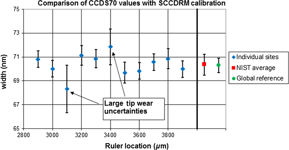 Generally, and as expected, CD-AFM1 tended to exhibit greater tip wear than is typical for the other two instruments. To estimate the standard uncertainty due to tip wear, we used a rectangular distribution with the before and after tip width values as end points. For about half of the results shown in Fig. 1, the tip wear was a significant contributor to the expanded uncertainty. For the results obtained at the 3100- and ruler locations, the observed tip wear was unusually large, but no specific reason for this is known. Nevertheless, the values all still agree within the uncertainties. The overlap of the NIST average result and expanded uncertainty, using the SCCDRM tip width calibration, with the CCDS calibration indicates consistency between the two independent calibrations. This agreement can also be seen in Table 1. In late 2010, CD-AFM3 was installed at NIST. After completing the calibration and characterization of the tool, we measured the CCDS70 sample again. However, we immediately encountered a difficulty: the CCDS70 sample appeared to have been altered from its original condition, perhaps due to contamination. Our experience with this standard and contamination is discussed further in the Appendix on sample handling, storage, and cleaning. As part of our original comparison in 2006, we evaluated the local linewidth roughness (LWR) or nonuniformity of the CCDS samples and the NIST SCCDRMs. As mentioned above, each width value shown in Fig. 1 represents the average of linewidth calculated from each of the 80 line scans of the corresponding image. The standard deviation of the line scan results of each image can be used to estimate the local nonuniformity or LWR. These LWR results are shown in Fig. 2, along with the equivalent estimates from the 2011 data and those from the 2016 data, which were obtained after a cleaning procedure discussed below and in the Appendix. Fig. 2Measurements of the apparent local width nonuniformity or LWR of the CCDS70 at different locations along the feature. The 2006 and 2011 results were taken in approximately the same locations, showing the increase in apparent LWR, probably due to particulate contamination. The 2016 results, obtained after cleaning, were from 10 different locations, of unknown position relative to the 2006 and 2011 sites because of damage to the navigation aids. 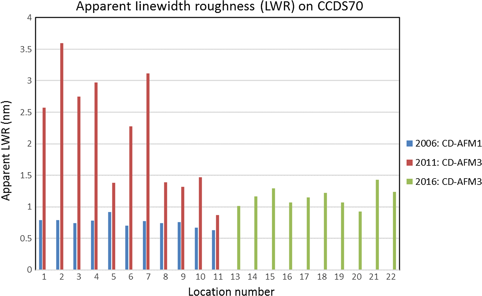 The apparent LWR results in Fig. 2 indicate a significant problem with the sample during the 2011 measurements. Despite this problem, however, the average result shown in Table 1 was still in agreement with the original CCDS calibration. This is somewhat counterintuitive since it means that the contamination had the effect of increasing LWR but not increasing the average width. This is not fully understood, although we suspect that an increased moisture level on the feature, which would affect the tip–sample interaction, is the probable reason for this observation. Subsequent to the discovery of this problem and since the CCDS70 was not part of our routine tool monitoring, it was removed from usage until we decided to risk cleaning it. This resulted in further damage to the cassette and the removal of the actual chip from the cassette. Additionally, the navigation aids (rulers), which were part of the cassette, were also destroyed. However, once it was removed from the broken cassette, cleaning of the CCDS70 chip was very easy. The apparent LWR results of the 2016 measurements shown in Fig. 2 suggest that the cleaning procedure was generally effective. The detailed results of the 2016 measurements are shown in Fig. 3. Due to the destruction of the navigation rulers, these locations could not be correlated with the original measurement sites, but they were similarly spaced along an undamaged length of the CCDS70 feature. The sampling plan was otherwise the same. Each image consisted of 80 scan lines distributed along . The only difference is that type CDR50 (nominal 50-nm width CD tips) tips were used. The bottom line from the measurements on the CCDS70 is that the SCCDRM and CCDS calibrations were demonstrated to be in agreement over 10 years and using two different CD-AFMs. Fig. 3Measurements of the width of the CCDS70 at different locations using the CD-AFM3 measurements taken in 2016 and calibrated with the SCCDRM. The results all agree within the expanded uncertainties (). The NIST average result and the independent global reference value provided by the vendor are both shown on the right and are in agreement. Note that the thick line separating the values on the right side is meant to emphasize that the NIST average and global reference values are not location specific. 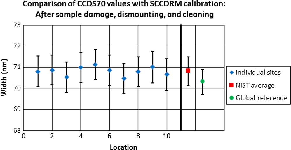 2.4.Measurements on the CCDS45 SampleA CCDS45 was initially measured by NIST using CD-AFM2 (at SEMATECH) in 2006,14 and it was measured again in 2011 and 2016 using CD-AFM3 at NIST. Like the CCDS70 sample, the initial goal of the measurements was to check the agreement between the independent TEM calibrations of the SCCDRM and CCDS. Subsequent measurements were performed to evaluate the long-term stability of the samples and their performance on different generation CD-AFM platforms. A summary of our measurements on the CCDS45 sample is given in Table 2. Table 2Summary of results on CCDS45 using CD-AFM2 and CD-AFM3.
Figure 4 shows the agreement of the SCCDRM and CCDS45 calibrations. The plot shows the individual linewidth measurements of the CCDS45 using CD-AFM2 and the expanded uncertainty of each measurement. The SCCDRM was used for tip width calibration. Type CDR70 tips (critical dimension, 70-nm nominal width) were used for the measurements shown in Fig. 4. The sampling plan was otherwise the same as used for the CCDS70 sample. Each result, shown at a ruler location in Fig. 4, represents the average of the linewidths taken from all line scans in the corresponding image. These images were taken at intervals along the available length of the feature. The independently derived CCDS calibration is shown on the right side of the plot as the global reference value with expanded uncertainty () limits, and the average of all the individual NIST measurements is shown to the left of this value. The overlap of the NIST results and the CCDS calibration is very good, indicating consistency between these two independent calibrations, as was the case for the comparison of the CCDS70. Fig. 4Measurements of the width of the CCDS45 at different locations using the CD-AFM2 measurements taken in 2006 and calibrated with the SCCDRM. The results all agree within the expanded uncertainties (). The NIST average result and the independent global reference value provided by the vendor are both shown on the right and are in agreement. Note that the thick line separating the values on the right side is meant to emphasize that the NIST average and global reference values are not location specific. 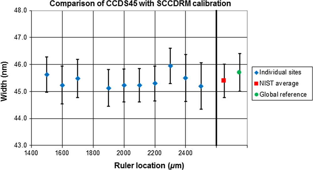 Subsequent to the installation of CD-AFM3 at NIST, we also checked the CCDS45 sample again. This spot check consisted of three sites between the 2100- and ruler locations. Type CDR50 tips were used for these measurements with the same image size. The average result is included in Table 2, and it is in good agreement with the CCDS calibration and the 2006 result. More recently, we attempted to duplicate the original 2006 measurement plan as closely as possible. The detailed results of these 2016 measurements are shown in Fig. 5. Type CDR50 tips were used for these measurements, and the same sampling plan (80 scan lines over ) was otherwise used. Although the overall results are in good agreement between Figs. 4 and 5, a site-by-site comparison of the results in Figs. 4 and 5 does not show the same pattern. This is probably due to inexact overlap of the 2006 and 2016 measurement windows and to differences in the effective tip wear (or contamination) at each measurement site. The estimated uncertainties capture the likely magnitude of the tip wear bias for each site, but the actual site-to-site value is variable. Despite this site-by-site difference, however, the overall CD-AFM3 measurements on the CCDS45 show that the SCCDRM and CCDS calibrations are in agreement over 10 years using two different CD-AFMs. Fig. 5Measurements of the width of the CCDS45 at different locations using the CD-AFM3 measurements taken in 2016 and calibrated with the SCCDRM. The results all agree within the expanded uncertainties (). The NIST average result and the independent global reference value provided by the vendor are both shown on the right and are in agreement. Note that the thick line separating the values on the right side is meant to emphasize that the NIST average and global reference values are not location specific. 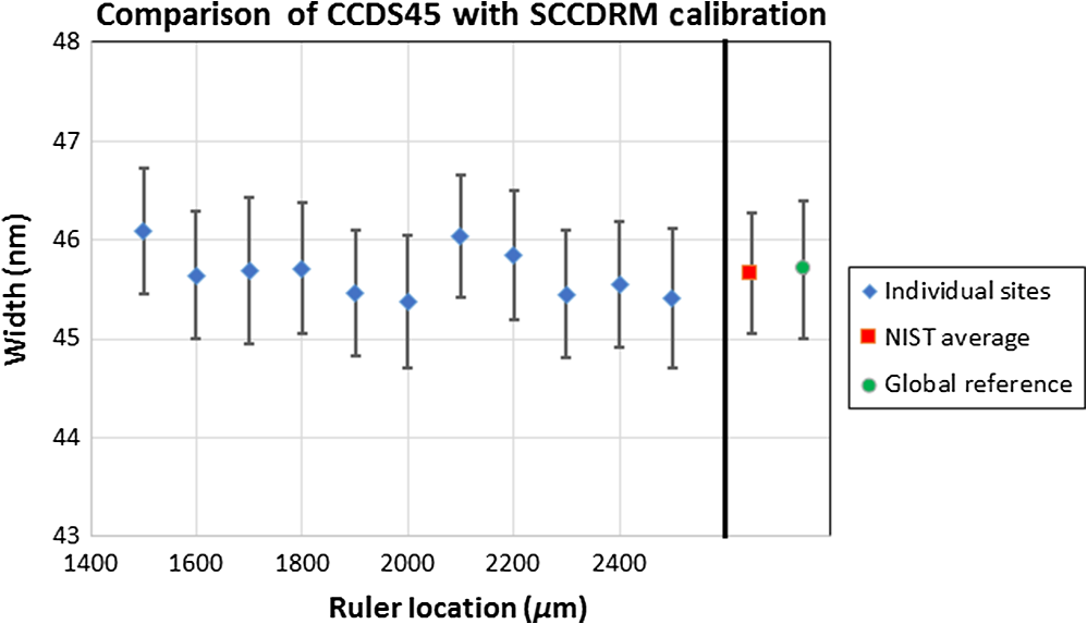 3.Discussion and SummaryIn this work, we have extended our previous results14 that demonstrated agreement between two independent realizations of the SI meter—both based on HRTEM. A comparison of this sort bolsters confidence in both results. However, additional comparisons, especially those involving other methods, can strengthen confidence even further and potentially reduce uncertainties. At the time of the original SCCDRM development, the HRTEM-based calibration was in agreement with a prior result based on the use of a knife-edge tip characterizer, but the SCCDRM calibration represented about a factor of 5 reduction of the uncertainty. Subsequently, we have performed additional validation experiments using HRTEM, and we have also used an entirely different mode of TEM operation: annular dark-field scanning transmission electron microscopy (ADF-STEM).6,17 The observed agreement is important because the contrast mechanisms of HRTEM and ADF-STEM are very different.20 In addition to these NIST experiments, we have also recently completed a comparison with PTB. The independently developed PTB result was also based on scanning transmission electron microscopy (STEM).11,12 The results of this comparison indicated agreement between NIST and PTB.21 All of the additional comparisons and validation experiments that we have performed so far are in agreement. However, owing mainly to the challenges of TEM image interpretation and edge detection, we have not yet been able to reduce the original SCCDRM uncertainties. Specifically, a critical issue in TEM interpretation is fringe contrast at the edges and selection of the appropriate intensity level to correspond with the edge. In the original NIST work on the SCCDRM calibration,5 a threshold selection of 50% relative intensity was implicitly made to evaluate the transition from the oxide layer to the encapsulating layer. However, for HRTEM images of those samples, this choice was largely empirical and did not have a specific theoretical basis. In the more recent PTB work using STEM,11 an analogous selection of threshold was made. At least heuristically, by analogy with incoherent optical microscopy, there is a theoretical basis for this selection. Recent improvements in both TEM instruments and sample preparation, particularly with respect to navigation and throughput, should facilitate further investigation of such questions, and both PTB and NIST plan to continue work in this area. In summary, using three different CD-AFM instruments located at both NIST and SEMATECH, we performed a width comparison of CCDS45 and CCDS70 specimens with the SCCDRM tip width calibration. Our observations verified the agreement and stability over a 10-year time period of these two independent HRTEM-based calibrations. This demonstrates not only the physical stability of the samples but also that this method of implementing a tip width metric for CD-AFM is, as would be expected, independent from the specific instrument utilized. Consequently, there are, in principle, no barriers to tool matching that would result from the use of different instruments at different sites. AppendicesAppendix:Mounting, Handling, Storage, and Cleaning of Critical Dimension StandardsCD-AFMs are generally designed to accommodate measurements on intact whole wafers, typically 200 or 300 mm but now including 450-mm wafers. Many tools are also capable of handling photomasks, although this usually requires a chuck change. One important consequence of this design for whole wafers is that it typically requires additional steps and effort to measure smaller or otherwise nontypical samples, such as chips or pieces of a wafer. Most CD-AFMs also include a holder, usually mounted adjacent to the chuck, with removable pedestals upon which small samples—up to about —can be mounted. Current systems usually have the capacity to accommodate seven pedestals, although at least five of these are normally allotted to vendor-supplied samples that are used for routine tool characterization. Since these pedestals are removable, however, it is always possible to accommodate mounting of a user sample in this manner. This possibility was taken into account when the original form factor of the SCCDRM was chosen, and some SCCDRMs have been installed in this manner by users. However, an even more common method of accommodating small samples/chips is to mount them on top of a scrap wafer, which functions as a carrier. While epoxy can be utilized for this purpose, we typically use the adhesive carbon tape that is popular among SEM users for mounting samples on SEM stubs. We have used both 200- and 300-mm wafers as carriers for this purpose, and, for some tools, it is still possible to use the automated wafer handling capabilities of the system with samples mounted on a wafer, although caution should always be used. During most of our SCCDRM development work and experimentation, we have used 200-mm carrier wafers and carbon tape to meet our sample mounting requirements, and this has generally been very successful. However, user errors are possible, and one occurred during the mounting of the CCDS70 cassette on a 200-mm carrier wafer, which resulted in a fractured cassette. After mounting, it was possible to measure the sample in CD-AFM1 without difficulty, but the fractured cassette was a source of particles and, combined with a failure of environmental control in storage, the CCDS70 was no longer viable for primary use at the time of the 2011 measurements. Sample storage is also an important factor, and we have encountered some challenges in this regard. The majority of CD-AFM tools are operated in manufacturing clean rooms with well-controlled environments—with respect to temperature and humidity—and are at a significantly lower risk of particulate contamination than those in typical laboratory environments. In these cases, special care may not be needed beyond the storage of the carrier wafer inside a wafer box or clamshell-style holder. However, for CD-AFM systems operated in laboratory environments, greater caution may be appropriate, particularly if significant transients in temperature, humidity, or particulates in the environment are anticipated. Our current instrument, CD-AFM3, is installed in the Advanced Measurement Laboratory facility at NIST. When the air handling is operating normally, our laboratory environment is held at and relative humidity (RH). Transients of and 10% RH are observed. The room air also undergoes high-efficiency particulate air filtration, and the instrument is enclosed in a soft-shell clean room that is nominally class 1000 but usually performs better than that. The reliability of our site-wide utilities (e.g., house vacuum, nitrogen, compressed air, and chilled water) is generally excellent, but this is partially achieved through regularly scheduled maintenance outages of these utilities, including the air handlers. These outages require users of individual laboratories to properly prepare equipment and storage facilities during these outages. We have occasionally experienced failures of our equipment, such as supplemental fans, dry boxes, and desiccated storage. Sufficient transients in laboratory temperature and RH combined with a degradation of sample storage conditions have led to condensation/moisture type contamination events on some of our samples. Among experienced practitioners of CD-AFM, the effects of moisture and other sticky contamination on the imaging performance of a CD-AFM are usually understood. However, since relatively little data have been published with respect to this, newcomers to the field may be caught unaware. Generally, the scanning behavior on such surfaces looks noisy and is intuitively suggestive of the tip sticking to and then pulling away from the surface. An example of this sort of scanning behavior, obtained using CD-AFM1 on developmental generation of the NIST SCCDRM, is shown in Fig. 6. It is worth mentioning that some unbaked photoresists may exhibit similar “sticky” scanning problems, particularly when using first-generation CD-AFMs. Fig. 6Example of severe scanning instability of CD-AFM1 on a moisture contaminated sample. This sort of problem can normally be eliminated with a vacuum bake of up to 200°C. For some contaminants, cleaning with basic solvents, such as ethanol, may be beneficial. 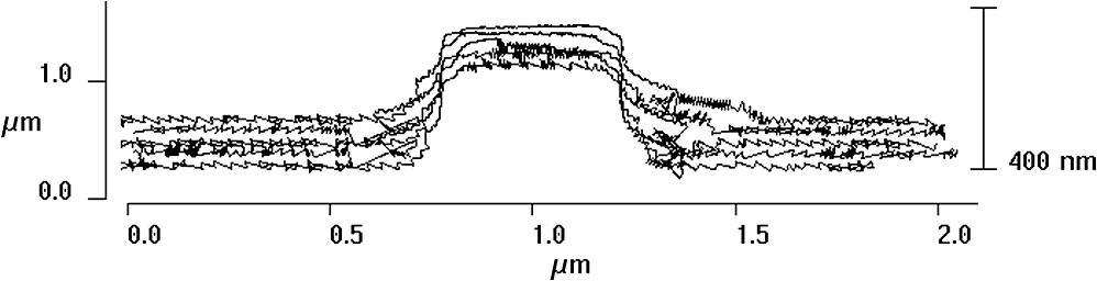 In cases where moisture alone is the problem, a simple vacuum bake can resolve this. We have successfully used a 60.0°C bake of an entire 200-mm carrier wafer with mounted samples on it to resolve this type of scanning problem. We were limited to 60.0°C in that case because the mounting adhesive was not rated for higher temperatures. Stubborn cases with more contamination may require an ethanol or isopropanol rinse followed by a 200.0°C bake. Generally, this procedure has also been very effective on our SCCDRMs and other AFM samples, at least for condensation and/or loosely attached particles/contaminants. It was the procedure we used successfully on the CCDS70 sample. We suspected the presence of particles, and the original mounting damage to the cassette forced us to remove the small chip from the cassette for any type of cleaning. This very basic method of cleaning is not usually sufficient for dealing with the much more challenging problem of hydrocarbon deposition that may occur in an SEM. This general phenomenon has been known for several decades and has been an important issue in CD-SEM metrology since at least the 1990s.22–25 The severity of the contamination effect depends on the cleanliness of the sample and the SEM chamber. There are increasingly advanced methods of mitigating this problem, but it is very difficult to eliminate entirely.25,26 For this reason, it is not generally recommended that CD-AFM calibration standards be exposed to SEM measurements. Samples that do have hydrocarbon contamination may require a much more aggressive cleaning process, such as the so-called “piranha” () clean. In addition to a basic solvent cleaning, we have also experimented with more aggressive methods. Ultraviolet ozone cleaning is potentially useful for some types of mild hydrocarbon contamination. Ultrasonic cleaning can also be very effective but also has significant risk of damage. In most semiconductor applications, the trend for this type of cleaning technology is toward the use of higher frequencies—up to 1000 kHz—usually called megasonic cleaning.27 The basic physical mechanism of cleaning is due to cavitation in the cleaning solution. Lower frequencies yield fewer but larger and more energetic bubbles and thus a more aggressive process, whereas higher frequencies yield many more but smaller and less energetic bubbles and thus a gentler process. Most laboratory or benchtop cleaners, however, use lower frequencies—typically 40 kHz—which have significant damage potential to nanostructures. Subsequent to the measurements of the CCDS70 shown in Fig. 3, we attempted an ultrasonic cleaning of the sample using our 40-kHz benchtop cleaner, but the cleaning was too aggressive and there was significant damage to the sample. Generally, we would recommend that 40-kHz ultrasonic cleaning is used conservatively; if a higher frequency unit is readily available, it should be tried first. AcknowledgmentsThis work was supported by the Engineering Physics Division of the NIST Physical Measurement Laboratory. ReferencesY. Martin and H. K. Wickramasinghe,
“Method for imaging sidewalls by atomic force microscopy,”
Appl. Phys. Lett., 64 2498
–2500
(1994). http://dx.doi.org/10.1063/1.111578 APPLAB 0003-6951 Google Scholar
X. Qian and J. S. Villarrubia,
“General three-dimensional image simulation and surface reconstruction in scanning probe microscopy using a dexel representation,”
Ultramicroscopy, 108 29
–42
(2007). http://dx.doi.org/10.1016/j.ultramic.2007.02.031 ULTRD6 0304-3991 Google Scholar
F. Tian, X. Qian and J. S. Villarrubia,
“Blind estimation of general tip shape in AFM imaging,”
Ultramicroscopy, 109 44
–53
(2008). http://dx.doi.org/10.1016/j.ultramic.2008.08.002 ULTRD6 0304-3991 Google Scholar
V. A. Ukraintsev et al.,
“Distributed force probe bending model of CD-AFM bias,”
J. Micro/Nanolithogr. MEMS MOEMS, 12 023009
(2013). http://dx.doi.org/10.1117/1.JMM.12.2.023009 Google Scholar
R. G. Dixson et al.,
“Traceable calibration of critical-dimension atomic force microscope linewidth measurements with nanometer uncertainty,”
J. Vac. Sci. Technol. B, 23 3028
–3032
(2005). http://dx.doi.org/10.1116/1.2130347 JVTBD9 1071-1023 Google Scholar
N. G. Orji et al.,
“Transmission electron microscope calibration methods for critical dimension standards,”
J. Micro/Nanolithogr. MEMS MOEMS, 15 044002
(2016). http://dx.doi.org/10.1117/1.JMM.15.4.044002 Google Scholar
G. A. Dahlen et al.,
“TEM validation of CD-AFM image reconstruction,”
Proc. SPIE, 6518 651818
(2007). http://dx.doi.org/10.1117/12.711943 Google Scholar
G. Dahlen et al.,
“Tip characterization and surface reconstruction of complex structures with critical dimension atomic force microscopy,”
J. Vac. Sci. Technol. B, 23 2297
–2303
(2005). http://dx.doi.org/10.1116/1.2101601 JVTBD9 1071-1023 Google Scholar
M. Tortonese et al.,
“Sub-50-nm isolated line and trench width artifacts for CD metrology,”
Proc. SPIE, 5375 647
–656
(2004). http://dx.doi.org/10.1117/12.536812 PSISDG 0277-786X Google Scholar
M. Cresswell et al.,
“RM8111: development of a prototype linewidth standard,”
J. Res. Natl. Inst. Stand. Technol., 111 187
–203
(2006). http://dx.doi.org/10.6028/jres JRITEF 1044-677X Google Scholar
G. Dai et al.,
“Reference nano-dimensional metrology by scanning transmission electron microscopy,”
Meas. Sci. Technol., 24 085001
(2013). http://dx.doi.org/10.1088/0957-0233/24/8/085001 MSTCEP 0957-0233 Google Scholar
G. Dai et al.,
“Development and characterisation of a new linewidth reference material,”
Meas. Sci. Technol., 26 115006
(2015). http://dx.doi.org/10.1088/0957-0233/26/11/115006 MSTCEP 0957-0233 Google Scholar
V. A. Ukraintsev et al.,
“The role of AFM in semiconductor technology development: the 65 nm technology node and beyond,”
Proc. SPIE, 5752 127
(2005). http://dx.doi.org/10.1117/12.602758 Google Scholar
R. Dixson and N. G. Orji,
“Comparison and uncertainties of standards for critical dimension atomic force microscope tip width calibration,”
Proc. SPIE, 6518 651816
(2007). http://dx.doi.org/10.1117/12.714032 Google Scholar
J. A. Kramar, R. Dixson and N. G. Orji,
“Scanning probe microscope dimensional metrology at NIST,”
Meas. Sci. Technol., 22 024001
(2011). http://dx.doi.org/10.1088/0957-0233/22/2/024001 MSTCEP 0957-0233 Google Scholar
N. G. Orji et al.,
“Progress on implementation of a reference measurement system based on a critical-dimension atomic force microscope,”
J. Micro/Nanolithogr. MEMS MOEMS, 6 023002
(2007). http://dx.doi.org/10.1117/1.2728742 Google Scholar
R. Dixson et al.,
“Traceable calibration of a critical dimension atomic force microscope,”
J. Micro/Nanolithogr. MEMS MOEMS, 11 011006
(2012). http://dx.doi.org/10.1117/1.JMM.11.1.011006 Google Scholar
Guide to the Expression of Uncertainty in Measurement, International Organization for Standardization, Geneva
(1995). Google Scholar
B. N. Taylor and C. E. Kuyatt, Guidelines for Evaluating and Expressing the Uncertainty of NIST Measurement Results, Washington(1994). Google Scholar
A. C. Diebold et al.,
“Thin dielectric film thickness determination by advanced transmission electron microscopy,”
Microsc. Microanal., 9 493
–508
(2003). http://dx.doi.org/10.1017/S1431927603030629 MIMIF7 1431-9276 Google Scholar
G. Dai et al.,
“Comparison of line width calibration using critical dimension atomic force microscopes between PTB and NIST,”
Meas. Sci. Technol., 28 065010
(2017). http://dx.doi.org/10.1088/1361-6501/aa665b MSTCEP 0957-0233 Google Scholar
J. Allgair et al.,
“SPC tracking and run monitoring of a CD-SEM,”
Proc. SPIE, 3332 243
(1998). http://dx.doi.org/10.1117/12.308732 Google Scholar
A. G. Deleporte et al.,
“Benchmarking of advanced CD-SEMs against the new unified specification for sub-0.18 micrometer lithography,”
Proc. SPIE, 4181 42
(2000). http://dx.doi.org/10.1117/12.395750 Google Scholar
B. D. Bunday and M. Bishop,
“Specifications and methodologies for benchmarking of advanced CDSEMs at the 90 nm CMOS technology node and beyond,”
Proc. SPIE, 5038 1038
(2003). http://dx.doi.org/10.1117/12.483663 Google Scholar
A. E. Vladár, M. T. Postek and R. Vane,
“Active monitoring and control of electron beam induced contamination,”
Proc. SPIE, 4344 835
(2001). http://dx.doi.org/10.1117/12.436724 Google Scholar
A. E. Vladár, K. P. Purushotham and M. T. Postek,
“Contamination specification for dimensional metrology SEMs,”
Proc. SPIE, 6922 692217
(2008). http://dx.doi.org/10.1117/12.774015 Google Scholar
P. Nesladek, S. Osborne and T. Rode,
“Comparison of cleaning processes with respect to cleaning efficiency,”
Proc. SPIE, 7985 79850P
(2011). http://dx.doi.org/10.1117/12.895198 Google Scholar
BiographyRonald Dixson is a physicist in the Physical Measurement Laboratory (PML) of the National Institute of Standards and Technology (NIST). His current research interests are calibration methods, traceability, and uncertainty analysis in atomic force microscope (AFM) dimensional metrology – including the NIST traceable AFM (T-AFM) project and metrology applications of critical dimension AFM (CD-AFM). He holds a PhD in physics and is a member of SPIE, AVS, and the American Physical Society. |
||||||||||||||||||||||||||||||||||||||||||||||||||||||||||


