
|
|
1.IntroductionMicrofluidic systems have attracted significant attention during the past decade because of their wide applications in biology1–4 and chemistry.5–7 In the photolithography process used to fabricate these microfluidic systems, usually a laser mask writer and a quartz or soda line glass mask are required. Unfortunately, these masks are expensive and require a cleanroom environment. To reduce these costs, in our approach we present a method for using laser-patterned wax-covered plastic paper as both the mask for deep-UV exposure and the shadow mask for metal sputtering. Polymer-based microfluidic devices can be fabricated in several ways, such as laser ablation,8–10 hot embossing,11–13 injection molding,14–16 and deep-UV patterning.17–19 Polymers, such as polymethylmethacrylate (PMMA), are highly transparent and have very low autofluorescence over a wide spectral range,20 making it a well used material in microfluidics. The PMMA can be patterned in all the above ways; however, hot embossing and injection molding are high-volume methods and have high-tooling costs, making their applicability to a research environment low. Direct laser ablation is usually used for rapid prototyping, which produces rough channels surfaces and make the observation difficult. The deep-UV (254 nm) patterning can be performed in hours and produces smooth channel surfaces for easy observation. The PMMA absorbs radiation during the deep-UV exposure, which causes chain scissions and increased solubility. Exposed PMMA can be developed using a mixture of isopropanol alcohol (IPA) and water; this developer could be used not only for the microscale structure,21 but also for the nanoscale patterning of PMMA.22,23 In our previous work, instead of using the traditional mask during deep-UV patterning, we transferred printed wax layers to act as a deep-UV mask;19 however, edge quality was low. In comparison, the method described in this study allows for the patterning of both the channels, with improved edge quality, and electrode layers for microfluidic devices using wax-covered plastic paper. This simple technical innovation will enable the lab-on-chip community to use equipment they likely already have to rapidly prototype higher quality channels with integrated electrodes. 2.Fabrication ProcessThe fabrication process starts with wax-coating plastic paper: a thin layer of wax () was printed onto a 135-μm thick plastic paper using Phaser 8560D solid ink printer. The plastic paper is polyester paper with the thickness of 135 μm (Model PP5WASC, Southwest Binding Company, Maryland Heights, Missouri). The type of the wax ink is Genuine XEROX Solid ink 8560. The next step [Fig. 1(a)] is using this wax-covered plastic paper to make the mask for gold sputtering. We used a commercial laser system (Universal PLS 6.75, maximum power output is 75 W and the highest scan speed of ) to cut the desired patterns for the electrodes on this wax-covered plastic paper. During the cutting process, the power setting of laser is 37.5 W with the scan speed of . For the cutting process, the laser is working in pulse mode with the pulse setting at 1000 PPI (point per inch). Alternatively, a craft cutter used by some labs could be used for the mask patterning. The characteristic of the laser-patterned plastic paper will be discussed in detail in the next section. Fig. 1Fabrication process of a polymethylmethacrylate (PMMA)-based microfluidic system using laser-patterned wax masks. (a) Laser cutting of the wax-covered plastic paper, which works as a mask for sputtering. (b) Sputtering Au (50 nm). (c) Removal of the wax mask. (d) Laser cutting of the wax-coated plastic paper, which works as the mask for 254-nm deep-UV patterning. (e) Deep-UV exposure of PMMA. (f) The PMMA sheet after UV exposure and development. (g) Bonding, piping, and wiring. 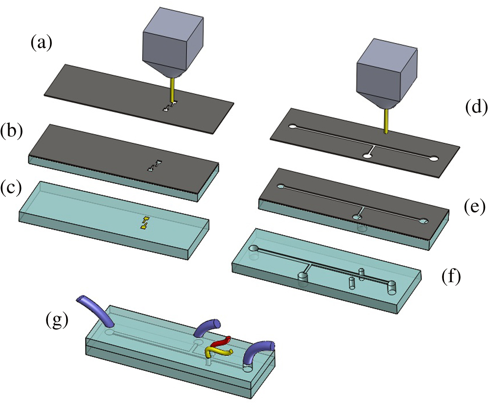 After the patterning, the wax-covered plastic paper which works as the mask was temporarily bonded to a 1-mm thick PMMA sheet (Lucite casted acrylic sheet) using a thermal laminator (Heatseal H600 Pro) at 76°C with the sample moving speed of [Fig. 1(b)]. The PMMA sheet covered with the mask was then sputtered with a 50-nm thick gold layer with a desktop sputtering system (Q300T, Quorum Technologies Ltd., East Sussex, United Kingdom); the sputter deposition current was set at 50 mA for 60 s at the vacuum of . Finally, the mask was peeled off, leaving behind the desired electrode pattern [Fig. 2(c)] on the PMMA sheet. After peeling off the mask, some residual wax may be left on the surface of PMMA which can be easily cleaned using Kimwipe lint free wipes. Fig. 2(a) Custom-made 254-nm deep-UV exposure box. (b) Laser-patterned wax-covered plastic paper used as a mask for the patterning of the microfluidic channel. (c) PMMA sheet after Au sputtering using the wax-covered plastic paper mask.  Another wax-covered plastic paper, which contains the microchannel patterns, was also fabricated using the laser system [Fig. 2(b)]. This mask was then thermally bonded to another 1-mm thick PMMA sheet (containing laser-ablated through holes) using the same method. After this bonding step, the PMMA sheet covered with wax plastic paper mask underwent a 4-h deep-UV exposure in a custom-made 254-nm deep-UV exposure box [Fig. 2(a)]; an inexpensive system like Stratagene’s Stratalinker UV Crosslinker can also be used. After the deep-UV exposure, the paper mask was peeled off, and the PMMA sheet was soaked in a 7:3 IPA:water solution for 20 min to develop the channels; this IPA and water solution will also help to remove any residual wax stuck to the PMMA sheet. The next step was bonding two PMMA sheets that contain gold electrodes and microfluidic channels, respectively. Thermal-compression bonding (INSTRON Dual Column Testing Systems) was conducted at 140°C (chamber temperature) with the pressure of 0.4 MPa for 50 min. The final process is wiring; wires were connected to the sputtered gold electrodes with the help of conductive glue (PELCO Conductive Silver 187). After the final process, the device was ready for testing. The device after fabrication process is shown in Fig. 3. 3.Experiment and DiscussionThe fabricated microfluidic device (Fig. 3) has T-shaped microchannels for droplet generation and two gold electrodes for droplet detection. Figure 4(a) shows the schematic of the droplet generation process, where the red liquid is water and the transparent liquid is mineral oil. When the oil droplet passes through the electrodes, the droplet will cause a brief change to the electrical resistance between the two electrodes. When the circuit is driven with a constant current, the drive voltage must correspondingly rise to maintain the current. By monitoring such pulses in electric current, the number of droplets can be counted (Coulter counter). Figure 4(b) shows the images of oil droplets generated in the microchannels. Fig. 4(a) Schematic diagram of the microfluidic system for droplet generation and detection. (b) Image of an oil droplet in a red-dyed water carrier generated in the PMMA microchannel.  We tested the minimum spacing for the laser cutting lines on wax-covered plastic paper before warping of the mask happens. The result shows that the spacing of cutting lines should not be smaller than 0.5 mm to avoid the warping happening. Figure 5 shows the laser cut with spacing of 0.5 and 0.4 mm, respectively; the severe warping happens when the spacing is smaller than 0.5 mm. On the other hand, slight warping of the plastic paper can be mended during the thermal lamination process mentioned in the previous section. The thermal lamination helps the plastic paper with a wax layer to stick onto the PMMA sheet, therefore mending the slight warping of the plastic paper. Theoretically, the minimum width of the laser-ablated line on the wax-covered plastic paper depends on the laser spot size after focusing. In the actual fabrication process, it is very hard to achieve this minimum width due to the nonoptimized focusing of the laser beam. Figure 6 was the scanning electron microscope (SEM) images showing microchannels on wax-covered plastic paper and corresponding microchannels on PMMA sheet after deep-UV exposure and development process. As shown in Fig. 6(b), the edge quality of the microchannels on the PMMA sheet was stable along the microchannels. Fig. 5The warping of plastic paper during the laser cutting on plastic paper. Minimum spacing of the cut line is 0.5 mm to avoid warping.  Fig. 6(a) The laser-cut patterns on wax-covered plastic paper. (b) Corresponding areas (junction of microfluidics channels) on PMMA sheet after development.  The deep-UV patterned microchannel has a smoother surface than laser-ablated microchannels. As shown in Fig. 7, the laser-ablated channels scatter light severely because of the roughness of the microchannel,24 making observation difficult. In contrast, the channel surface fabricated using UV patterning is smooth and allows easy observation. The main mechanism during the deep-UV exposure of PMMA is the cleavage of chemical bonds. Chemical bond cleavage in both the main chain and side groups was the result of the absorption of high-energy radiation. Chain scissions lead to a decrease in the average molecular weight, which leads to an increase in PMMA solubility, and allow the exposed areas to develop. For the deep-UV patterning process, chemical bond breaks were mainly due to the photon absorption, which creates a smooth gradient and thus a smooth surface. For the laser ablation method [Fig. 7(b)], the chemical bonds are broken photothermally and will cause melting and evaporation of PMMA. These violent reactions of melting and evaporation lower the surface quality of the microchannels. For comparison, the SEM images of the microchannels fabricated by deep-UV exposure and laser ablation were also shown in Fig. 8. Fig. 7Optical images of (a) the deep-UV fabricated channels on a 1-mm thick PMMA sheet and (b) laser-ablated microchannels on PMMA sheet.  Fig. 8SEM images of (a) the deep-UV fabricated channels on a 1-mm thick PMMA sheet and (b) laser-ablated microchannels on PMMA sheet.  Due to the not-collimated deep-UV light, there is a slight expansion of the features on the PMMA sheet during the deep-UV processing. Figure 9 compares the dimension of patterns on paper mask and the dimension for the microchannels after the development on PMMA sheet (laser power setting at 15 W with various laser scan speeds). On average, there is an expansion of the channel size on the PMMA with respect to the mask. This expansion is constant and can be easily compensated for by undersizing the desired feature by 80 μm on the mask. Figure 10 shows the cross-section of a representative deep-UV patterned channel with a width of 410 μm and a depth of 54 μm, as measured by a profilometer (AMBIOS XP-200), for which the corresponding developing rate is around . Fig. 10Profile measurement of the microfluidic channel on a 1-mm PMMA sheet after the deep-UV exposure and development.  The UV transmission of the wax layer and plastic paper was measured to verify the ability of wax-coated plastic paper to work as a shadow mask during the deep-UV process. At the wavelength of 254 nm, which was being used in the deep-UV pattering of PMMA, the plastic paper covered with a wax layer has a transmission of 0.833%, which makes it suitable for masking the deep-UV process. The plastic paper without wax covering has a UV transmission of 2.247% and a quartz sheet (1-mm thick, Ted Pella, Inc., Redding, California) covered with wax layer has a transmission of 0.853% at 254 nm of the wavelength. In the fabrication process, a wax-covered plastic paper was used as the mask for gold sputtering. Due to the spacing between the paper mask and PMMA substrate, the feature size is slightly enlarged during the gold-sputtering process. The comparison between the feature size of the mask and actual sputtered feature size is shown in Fig. 11. The thickness of the sputtered gold layer should not less than 50 nm to ensure a good adhesion on the PMMA surface. Experiment reveals that, if the gold layer is thinner than 50 nm, thermal crack will be generated on gold layer during the thermal compression bonding process. Fig. 11Comparison of the mask feature size and actual patterned (Au sputtering) feature size with the 1:1 reference line.  Microchannels on wax-covered plastic paper were patterned by a laser system, and the dimension of the microchannels depends on the laser power. Figure 12 shows the dimension of the microchannels on wax-covered plastic paper with various laser powers at three different laser scanning speeds. Generally, the size of the microchannel will increase with the higher laser power at the same scanning speed. On the other hand, the size of the microchannel will increase with a low laser scanning speed. Fig. 12Channel width comparison of the laser-ablated microchannels with various laser scan speeds and powers.  Signal measurement circuit of the demonstrated microfluidic system for droplet counting was shown in Fig. 13. A current of 1 mA from the current source (NI PXI-4130) was supplied between two gold electrodes with a series resistor of , and when the nonconductive oil droplet is passing through the electrodes, the circuit will be cut off. By measuring the voltage drop on resistor, we can count the droplets in our microfluidic system. The voltage measurement at the resistor was shown in Fig. 14, in which each peak representing a droplet passing through the electrodes. 4.ConclusionThis work provides a novel technique using wax-covered plastic paper that was laser micromachined for both the masks for deep-UV PMMA patterning and metal sputtering. This combination produces smoother channels with better surface quality and allows electrode integration. To demonstrate the feasibility of this technique, a droplet generator with electrodes for droplet detection and counting was fabricated. This process is simple, rapid, low cost, and does not require cleanroom facilities. Using tools that many microfluidics labs already have access to, this technical innovation allows for the fabrication of electrical connections to the reservoirs and high-quality microchannels. Low-cost microfluidic devices fabricated using this technique have many potential applications in biological and chemical analysis areas. ReferencesP. S. DittrichA. Manz,
“Lab-on-a-chip: microfluidics in drug discovery,”
Nat. Rev. Drug Discovery, 5
(3), 210
–218
(2006). http://dx.doi.org/10.1038/nrd1985 NRDDAG 1474-1776 Google Scholar
V. SrinivasanV. K. PamulaR. B. Fair,
“An integrated digital microfluidic lab-on-a-chip for clinical diagnostics on human physiological fluids,”
Lab Chip, 4
(4), 310
–315
(2004). http://dx.doi.org/10.1039/b403341h LCAHAM 1473-0197 Google Scholar
R. J. Meagheret al.,
“An integrated microfluidic platform for sensitive and rapid detection of biological toxins,”
Lab Chip, 8
(12), 2046
–2053
(2008). http://dx.doi.org/10.1039/b815152k LCAHAM 1473-0197 Google Scholar
D. FigeysD. Pinto,
“Lab-on-a-chip: a revolution in biological and medical sciences,”
Anal. Chem., 72
(9), 330 A
–335 A
(2000). http://dx.doi.org/10.1021/ac002800y ANCHAM 0003-2700 Google Scholar
Y. T. Tanget al.,
“Development and characterization of a microfluidic chamber incorporating fluid ports with active suction for localized chemical stimulation of brain slices,”
Lab Chip, 11
(13), 2247
–2254
(2011). http://dx.doi.org/10.1039/c1lc20197b LCAHAM 1473-0197 Google Scholar
R. M. Guijtet al.,
“Chemical and physical processes for integrated temperature control in microfluidic devices,”
Lab Chip, 3
(1), 1
–4
(2003). http://dx.doi.org/10.1039/b210629a LCAHAM 1473-0197 Google Scholar
K. AbeK. SuzukiD. Citterio,
“Inkjet-printed microfluidic multianalyte chemical sensing paper,”
Anal. Chem., 80
(18), 6928
–6934
(2008). http://dx.doi.org/10.1021/ac800604v ANCHAM 0003-2700 Google Scholar
H. Liet al.,
“Fabrication of polystyrene microfluidic devices using a pulsed laser system,”
Microsyst. Technol., 18
(3), 373
–379
(2012). http://dx.doi.org/10.1007/s00542-011-1410-z MCTCEF 0946-7076 Google Scholar
H. KlankJ. P. KutterO. Geschke,
“Laser micromachining and back-end processing for rapid production of PMMA-based microfluidic systems,”
Lab Chip, 2
(4), 242
–246
(2002). http://dx.doi.org/10.1039/b206409j LCAHAM 1473-0197 Google Scholar
M. Bowdenet al.,
“Laser microfabrication of an integrated polymer microfluidic manifold for the determination of phosphorus,”
Lab Chip, 3
(4), 221
–223
(2003). http://dx.doi.org/10.1039/b307655e LCAHAM 1473-0197 Google Scholar
A. Mathuret al.,
“Characterisation of PMMA microfluidic channels and devices fabricated by hot embossing and sealed by direct bonding,”
Curr. Appl. Phys., 9
(6), 1199
–1202
(2009). http://dx.doi.org/10.1016/j.cap.2009.01.007 1567-1739 Google Scholar
S. Qiet al.,
“Microfluidic devices fabricated in poly (methyl methacrylate) using hot-embossing with integrated sampling capillary and fiber optics for fluorescence detection,”
Lab Chip, 2
(2), 88
–95
(2002). http://dx.doi.org/10.1039/b200370h LCAHAM 1473-0197 Google Scholar
P. Shiuet al.,
“Rapid fabrication of tooling for microfluidic devices via laser micromachining and hot embossing,”
J. Micromech. Microeng., 18
(2), 025012
(2008). http://dx.doi.org/10.1088/0960-1317/18/2/025012 JMMIEZ 0960-1317 Google Scholar
V. Piotteret al.,
“Performance and simulation of thermoplastic micro injection molding,”
Microsyst. Technol., 8
(6), 387
–390
(2002). http://dx.doi.org/10.1007/s00542-002-0178-6 MCTCEF 0946-7076 Google Scholar
U. M. AttiaS. MarsonJ. R. Alcock,
“Micro-injection moulding of polymer microfluidic devices,”
Microfluid. Nanofluid., 7
(1), 1
–28
(2009). http://dx.doi.org/10.1007/s10404-009-0421-x 1613-4982 Google Scholar
D. A. Mairet al.,
“Injection molded microfluidic chips featuring integrated interconnects,”
Lab Chip, 6
(10), 1346
–1354
(2006). http://dx.doi.org/10.1039/b605911b LCAHAM 1473-0197 Google Scholar
D. SameotoC. Menon,
“Deep UV patterning of acrylic masters for molding biomimetic dry adhesives,”
J. Micromech. Microeng., 20
(11), 115037
(2010). http://dx.doi.org/10.1088/0960-1317/20/11/115037 JMMIEZ 0960-1317 Google Scholar
M. Haiducuet al.,
“Deep-UV patterning of commercial grade PMMA for low-cost, large-scale microfluidics,”
J. Micromech. Microeng., 18
(11), 115029
(2008). http://dx.doi.org/10.1088/0960-1317/18/11/115029 JMMIEZ 0960-1317 Google Scholar
Y. Fanet al.,
“Printed wax masks for 254 nm deep-UV pattering of PMMA-based microfluidics,”
J. Micromech. Microeng., 22
(2), 027001
(2012). http://dx.doi.org/10.1088/0960-1317/22/2/027001 JMMIEZ 0960-1317 Google Scholar
F. Baldiniet al.,
“An optical PMMA biochip based on fluorescence anisotropy: application to C-reactive protein assay,”
Sens. Actuators B: Chem., 139
(1), 64
–68
(2009). http://dx.doi.org/10.1016/j.snb.2008.08.027 SABCEB 0925-4005 Google Scholar
R. W. JohnstoneI. G. FouldsM. Parameswaran,
“Deep-UV exposure of poly (methyl methacrylate) at 254 nm using low-pressure mercury vapor lamps,”
J. Vac. Sci. Technol. B: Microelectron. Nanometer Struct., 26
(2), 682
–685
(2008). http://dx.doi.org/10.1116/1.2890688 JVTBD9 0734-211X Google Scholar
S. YasinD. G. HaskoH. Ahmed,
“Comparison of MIBK/ IPA and water / IPA as PMMA developers for electron beam nanolithography,”
Microelectron. Eng., 61–62 745
–753
(2002). http://dx.doi.org/10.1016/S0167-9317(02)00468-9 MIENEF 0167-9317 Google Scholar
S. YasinD. HaskoH. Ahmed,
“Fabrication of width lines in poly (methylmethacrylate) resist using a water: isopropyl alcohol developer and ultrasonically-assisted development,”
Appl. Phys. Lett., 78
(18), 2760
–2762
(2001). http://dx.doi.org/10.1063/1.1369615 APPLAB 0003-6951 Google Scholar
Z. K. Wanget al.,
“Improving surface smoothness of laser-fabricated microchannels for microfluidic application,”
J. Micromech. Microeng., 21
(9), 095008
(2011). http://dx.doi.org/10.1088/0960-1317/21/9/095008 JMMIEZ 0960-1317 Google Scholar
Biography Yiqiang Fan received his bachelor’s degree from Tianjin University and his master’s degree from King Abdullah University of Science and Technology (KAUST) in mechanical engineering, in 2009 and 2010, respectively. He is currently a PhD student in electrical engineering at KAUST. His research interests mainly lie in MEMS and microfluidics technologies, especially for low-cost and rapid fabrication techniques of polymer-based microfluidics systems.  Huawei Li received his PhD degree in physical chemistry from University of Calabria in 2009. In 2010, he joined Prof. Ian Fould’s group at KAUST as a postdoctoral fellow. His current research is focused on the development of novel microfabrication techniques and the applications of microfluidic devices with special interest using polymer materials as the substrates.  Ying Yi received his BS degree in Information Technology from HeBei Normal University, HeBei province, China, and an ME degree from the Department of Electronics and Radio Engineering, Kyung Hee University, Korea, in 2008 and 2010, respectively. Since 2012, he has been studying for the PhD degree in the Department of Electrical Engineering, King Abdullah University of Science and Technology (KAUST), Saudi Arabia. His research interests are wireless systems and micro-electro-mechanical systems (MEMS).  Ian G. Foulds is an assistant professor of electrical engineering at King Abdullah University of Science and Technology (KAUST). He earned his PhD in 2007 from Simon Fraser University, Canada. His research interests are in the area of microsystems fabrication with special interest in the use of polymer materials and low-cost fabrication techniques. He is the primary investigator of the Electromechanical Microsystems & Polymer Integration Research (EMPIRe) Group. |


