|
|
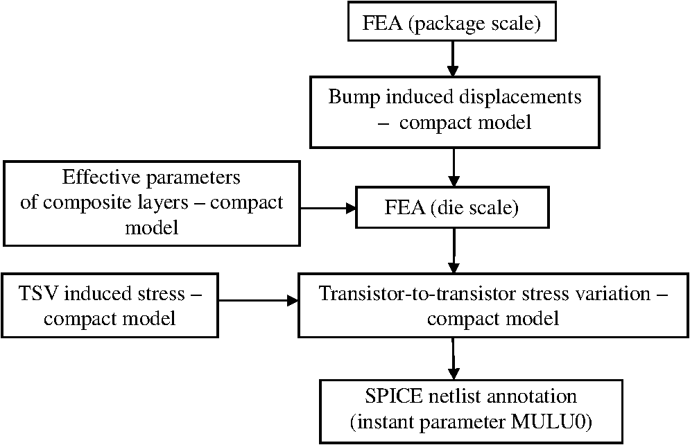
1.IntroductionIt is a common understanding that the motivation for 3-D IC integration is a mixture of economic and technical requirements, summarized within the term “More than Moore.”1–3 Three-dimensional (3-D) IC stacking technologies (including 2.5D interposer-based approaches), employing thinned wafer/through silicon via (TSV) structures, are novel solutions that result in reduced floor space, higher bandwidth, and reduced energy consumption. To enable 3-D chip stacking, new components were adopted by interconnect technology: through-silicon vias to provide connectivity between the back-end-of-line (BEoL) and back-chip redistribution layer (BRDL) metallization of some of the stacked dies, and solder or metal bumps and pillars for interconnecting the neighboring dies. The processing of high-density TSV structures through thinned dies and subsequent 3-D stacking is a promising technological alternative to the traditional two-dimensional (2-D) lithography/etch scaling. However, several issues have to be addressed to guarantee the needed product performance and reliability. Among them are management of mechanical stress and high Joule heating as well as reliability issues such as electromigration and stress migration.4 Many of the process steps employed by 3-D IC technology act as stress sources that can affect the chip performance and reliability. These are TSV etching and filling, wafer/die thinning, wafer bumping, high-temperature solder reflow, chip stacking, etc.3,5 Hence, it is important to have a capability to accurately assess the stress generated during 3-D IC stacking. The traditional chip–package interaction (CPI) concerns are related to reliability issues caused by high peeling and shear stresses (hundreds of MPa), which are able to cause cracking, delamination, etc., resulting in shorts or opens. These stresses represent a serious risk for chips’ durability; nevertheless, the existing measurement and screening procedures enable the failure modes detection, allowing to eliminate the detected threats. The failure risk can be minimized by using appropriate package assembly materials, which can decrease substantially the CPI stress. Analysis of the reliability issues is out of scope of this paper. The stress simulator described here reflects the needs of designers and manufacturers of 3-D IC chip packages to control deviations of design-in MOSFET parameters that cause degradation of the chip performance. Even relatively low values of CPI stress (less than hundred MPa) can cause parametric failures of circuits due to change of charge carrier mobility in transistor’s channel regions. Stress gradients across regions where circuits are located can worsen the chip performance even if the stress level is not high. Due to the lack of measurement and screening procedures for detecting mobility shift in transistors, the developed simulator becomes an additional metrology tool for 3-D IC package inspection. It is a very challenging task to get an entire picture of the modification of the stress distribution across device layers caused by 3-D IC technology. Different scales of the stress distributions must be taken into account: die scale (i.e., several millimeters) global stress variations which are generated due to thin die bending; bump and TSV scale (i.e., 10 to 100 μm) local stress variations, which are induced by the package component assembly; device scale (10 to 100 nm) variations due to transistor layer nonuniformity. Traditional methods such as finite-difference analysis and finite-element analysis (FEA) cannot be employed for a simulation of the transistor channel stress distribution across a die due to the size of a model, which can easily reach hundreds of millions degrees of freedom. The established FEA-based stress simulators have typically been used for addressing the traditional CPI effect where a silicon chip was modeled as a homogeneous isotropic piece of silicon. Details of chip structures (layer information, layout, etc.) have not been considered, and the problem with calculating the transistor-to-transistor intrachannel stress variation and consequent variation in transistor electrical characteristics has not been addressed yet.6 In order to be able to consider these effects, the stress simulation methodology should be capable to resolve scales of the order of a transistor size (approximately nanometers) and, to account for all major internal (layout-induced) and external (e.g., packaging) stress sources affecting a particular device. Compact model-based approaches for the layout-induced stress effects, which typically employ the empirical modeling,7,8 cannot take into account the package-induced variations in transistor characteristics. Because of the lack of physics-based foundation, this kind of modeling cannot provide a link to the physics-based package-scale simulation in order to include a CPI-induced stress loading. A look-up table methodology is not practical due to a large size of each device’s surrounding layout area (radius of up to 5 μm) that should be accounted for a correct stress prediction. It will require the generation of an enormous amount of local layout configurations around a gate in order to obtain a proper representation. Therefore, the development of compact physics-based models is the only possible solution to achieve the ultimate goal of predicting and simulating transistor-to-transistor stress variation across a device layer. These compact models are based on analytical treatment of the elasticity problems: approximate solutions of the basic differential equations are used to generate a set of simple algebraic equations allowing fast full-chip analysis of stress values in transistor channels. Resolved stress variation should be converted further into the variation of the device electrical characteristics. This paper describes the recently developed physics-based simulator that predicts variation in transistor’s electrical characteristics, caused by CPI. The simulator provides an interface between layout formats (GDS II, OASIS) and FEA-based package-scale models. 2.Simulation MethodologyThe proposed simulation methodology/flow, which will be discussed in detail below, results in the development of a new type of design verification tools. The tool is capable of analyzing any 3-D IC die stack design with regard to out-of-spec variations in device electrical characteristics caused by mechanical stress generated by warpages of the stacked dies, by solder bumps pressure generated in a course of die stacking, as well as by mismatch of thermomechanical properties of TSV and silicon die bulk. The target of the developed simulation flow is the calculation of across-die distributions of the stress normal components (i.e., diagonal components of stress tensor) inside transistor channels and its conversion into the stress-modified electrical characteristics of the transistors. This simulation flow, shown schematically in Fig. 1, can be described as a sequence of the simulation steps performed with different simulation tools:
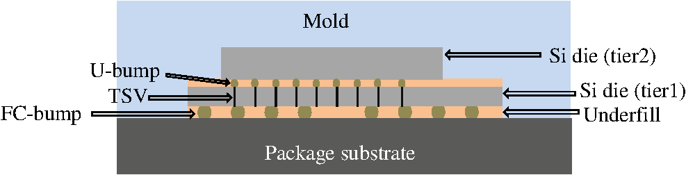
Both FEA simulations and compact modelling are performed assuming an elastic behavior of all materials involved in package assembly. The possibilities of plastic deformation of solder bumps and viscoelastic behaviour of interlayer dielectric and underfill are not considered in the presented simulation flow. Viscoelastic properties of underfill layer above glass transition temperature are not modeled assuming that the major input into stress caused by the bumps contact interactions with the dies (thin multilayered plates) was developed at temperatures below . Within the accepted linear theory of elasticity, the superposition of stresses induced by various assembly components can be used to obtain the total stress distribution. According to the flow schematics (Fig. 1), the stress created by TSVs is considered separately and is assumed to be independent of wafer deformation. Obviously, TSVs cannot be resolved in package scale FEA simulations (due to their small sizes), which implies that the possible effect of TSVs on assembly-induced wafer deformation is neglected. It should be mentioned that this effect is captured at the FEA die-scale simulation step by introducing the nonuniform, coordinate-dependent mechanical properties of the silicon die bulk layer governed by TSV locations. The described simulations methodology has resulted in the development of a flow for assessment of stress-induced variations in the carrier (electrons and holes) mobility in MOSFET channels, which, when it is plugged into the standard design flow, can be used for the design hot-spots screening and for accurate simulation of a variety of chip characteristics such as performance, leakage, power, etc. 2.1.Package-Scale FEA-Based SimulationAssembly of 3-D IC stack involves the wafer-to-wafer, or die-to-wafer or die-to-die mounting. Mechanical and electrical integrities of the stacked dies are achieved by employment of solder balls/metal pillars and TSVs (Fig. 2). Large flip-chip (FC) bumps connect the tier1 die to the substrate, while the set of TSVs and micro-bumps provide the die-to-die connection. The assembly of 2.5D packages is similar but involves only a die-to-interposer mounting. The encapsulation of the dies is performed by employment of an underfill resin in the gaps between dies, and finally molding the whole stack. Curing the package at high temperatures () and subsequent cooling down to room temperature create substantial thermal load, resulting in the bending (warpage) of the dies, due to mismatch of the thermomechanical parameters of different layers. This process generates large stresses in the dies, mainly due to large values of the coefficient of thermal expansion (CTE) of the underfill, which results in “shrinking” of silicon die in lateral directions. FEA-based simulation, which is a traditional method for analyzing a mechanical behavior of the package, is included in the developed flow. Another possible approach is an approximate analytical analysis of stresses in multilayered structures.9,10 A review of different types of analytical techniques available for resolving the stress-related problems in silicon technology was presented in Ref. 11. Although the analytical modeling can enable a fast computing of some of the stress components in 3-D IC stack, it is expected to be less accurate than the FEA analysis in the case when tiers of different lateral sizes are stacked in the package as shown in Fig. 2. Obviously, the FEA-based package simulation cannot resolve geometrically the effect of hundreds of FC-bumps and microbumps. Therefore, all layers in the stack are considered as the homogeneous thin plates. At this step, the thermomechanical characteristics of underfill layers are defined using the so-called rule of mixtures.12 This means that the bumps are assumed to be “smeared” throughout the entire layer. The mechanical characteristics of this “smeared” layer are obtained by the volume averaging of the corresponding properties of bumps and underfill in accordance with their volume fractions. An example of the simulated distribution of the stress components in two-tier stack across tier1 is shown in Fig. 3. This stress, which is generated due to mismatch in thermomechanical properties of the constituent layers, is accompanied by the warpage of the dies. With the thicknesses of the layers in the package and values of material properties collected in Table 1, the values of lateral components of the stress exceed 100 MPa. Larger stress can be generated with decreasing die thickness. Evidently, stress distribution is nonuniform near the edges of the analysed (tier1) die. In addition, a strong nonuniformity is observed in the region under the periphery of upper (tier2) die, which is caused by vertical pressure created by tier2 die edges. Fig. 3(a) The architecture of the analyzed die; (b) distribution of global stress components in tier1 across the subsurface region indicated in (a) by the dashed line. 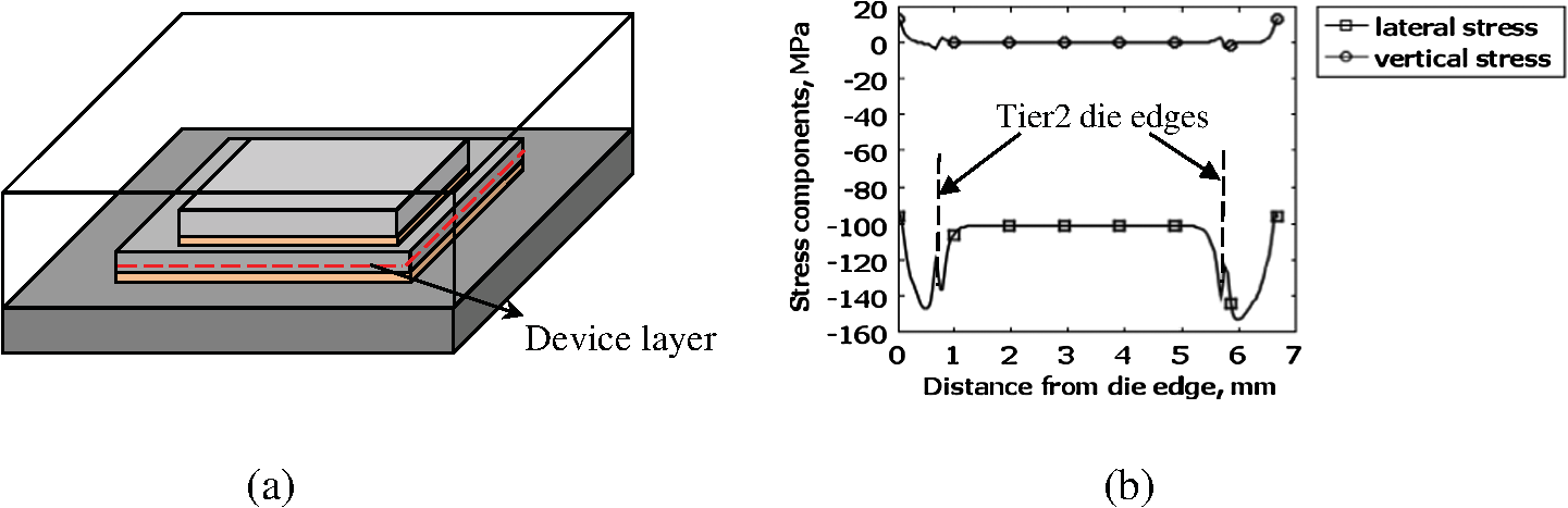 Table 1Thicknesses and thermomechanical properties of materials in the 3-D package used in FEA simulations.
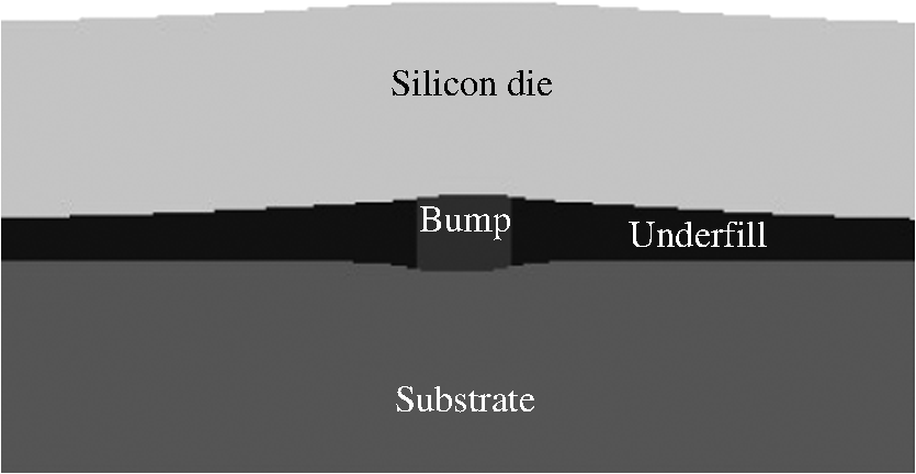
2.2.Compact Model for Bump-Induced DisplacementsAlthough the FEA simulation allows us to obtain the detailed variation of the warpage-induced stresses (Fig. 3), it does not take into account the local deformation/stress generated by bumps. To capture this deformation, an analytical modelling linked with the package-scale FEA simulation was developed. Fields of warpage-related displacements of the top and bottom surfaces of all layers calculated by FEA tool can be used for linking the package-scale simulations with the bump-scale model. These displacements allow calculating analytically the approximate local deformations generated around each bump. Here and below the displacement implies 3-D vector , which defines the stress components in the employed approximation of elastic materials. Figure 4 shows the local deformation that is generated around the FC bump due to chip cooling from the processing temperature down to operating temperature. Bumps, consisting of intermetallic compounds (in the case of FC bumps) or copper (micro-bumps), are characterized by the substantially larger Young’s modulus () than the underfill material (), i.e., , but by smaller CTE (i.e., ). As a result, the placement of the bump into the underfill layer should modify the warpage-related displacement fields both in lateral () and vertical () directions13 (Fig. 4). Due to a mismatch between the bump height shrinkage and the vertical deformation of the underfill at the bump location, both caused by the cooling, the bump acts as an indenter deforming both the substrate and die subsurface regions in the case of FC bumps. A vertical load generated by the bump can be written as Here, is the bump height, represents warpage-related vertical strain at the bump location, and describes the thermal load. Similarly, due to warpage-induced lateral displacements , each bump generates the following tangential load where is the bump diameter, and represents warpage-related lateral strain in the bump region. It should be mentioned that the thermal mismatch of bump and underfill is able to reduce the tangential load provided by Eq. (2). Besides, an extra load is generated by the shear deformation of the bumps, which originates due to different CTE of the silicon die and of the substrate. This shear component of bump deformation is more essential for the bumps located near the die edges. Formulas (1) and (2) establish the link between the bump compact model-induced displacements and the warpage-related displacements calculated with the FEA model.The additional deformation of the die surface due to loading Eqs. (1) and (2) can be calculated by solving the corresponding problems of contact mechanics.14,15 Additional field of -displacements at the die surface that is generated by a single bump is Here, is the distance to the center of the bump, and are the complete elliptic integrals of the first and second kinds correspondingly, with modulus , and and are the Young’s modulus and Poisson’s factor of the material which is in contact with the bump. Taking into account a fast decay of the bump contribution to the total vertical displacements at large distance , we have introduced an effective “radius of bump interaction” , which restricts the size of the area affected by the bump. This estimates the bump model accuracy. Similarly to Eq. (3), the lateral displacements caused by loads (1) and (2) can be obtained by using the force-balance equation based analysis. Finally, the total displacements at the die surfaces can be obtained by adding the bump-induced displacements to warpage-induced one : Equation (4) shows that all bumps at within the region affect the displacement generated at this point. 2.3.Effect of Nonuniform Interconnect, BRDL and Silicon Bulk Mechanical Characteristics on the CPI-Induced Stress Simulated with the Die-Scale FEA ModelStrain and stress distribution across a device layer, which is a layer located in the silicon interior just nanometers below the interface with the BEoL interconnect, should be calculated with a FEA tool by implementing the field of displacements (4) as the boundary conditions (BCs) for the die faces. At this step, each die is considered as a multilayer stack consisting of a silicon layer, BEoL interconnect, and BRDL layers. These layers are characterized by the nonuniform spatial distributions of the elastic and thermal properties determined by their layouts. An assessment of additional stress variation caused by the nonuniformity of the mechanical properties of these layers is implemented in the developed simulation flow. A calculation methodology of the effective Young’s modulus, Poisson’s ratio, and CTE as functions of metal density in each metal layer has been developed based on the theory of mechanical properties of anisotropic composite materials.12 This methodology requires a division of all considered composite layers into a number of bins. Average values of thermomechanical properties of the composite material are calculated for each bin on the basis of the average metal density inside the bin. The size of the bin should be chosen based on required simulation accuracy: the finer partitioning provides more accurate results at the expense of the run time. Depending on routing direction of the metal wires, the Young’s modulus of ’th bin at ’th layer should be calculated using one of the following formulas:12 where the symbols and denote directions parallel and perpendicular to routing direction correspondingly; and are Young’s modulus of metal and interlayer dielectric. The similar approach is used for calculating Poisson’s ratio and CTE of all composite layers.FEA model is used for the die-scale simulation of the stress components . In this simulation, the BCs are represented by previously calculated die face displacements, and the material properties are represented by the calculated position-dependent mechanical properties of the composite layers: Figure 5 demonstrates the distributions of stress components across the device layer of tier1 of the stack shown in Fig. 3(a). The studied region is located far from the die edges; therefore, the obtained periodical distribution of the stress components reflects a periodical pattern in bump locations. Across die variation of the BEoL mechanical properties results in the stress distribution blurring. The colormaps, showing stress values in Fig. 5, were obtained using the material properties presented in Table 1 and the properties of the bumps, interlayer dielectric (ILD), and copper presented in Table 2. Fig. 5An example of the die-scale simulation results: distributions of stress components across the device layer of tier1 die. The obtained patterns are due to the effect of FC bumps of 80-μm diameter. The size of the demonstrated region is . 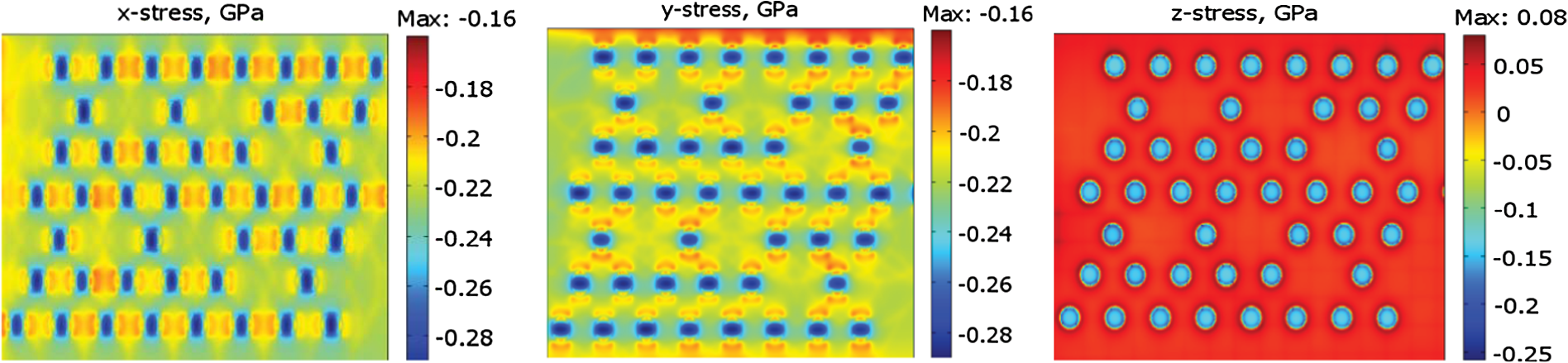 Table 2Thermomechanical properties of bumps and back-end-of-line (BEoL) interconnect materials.
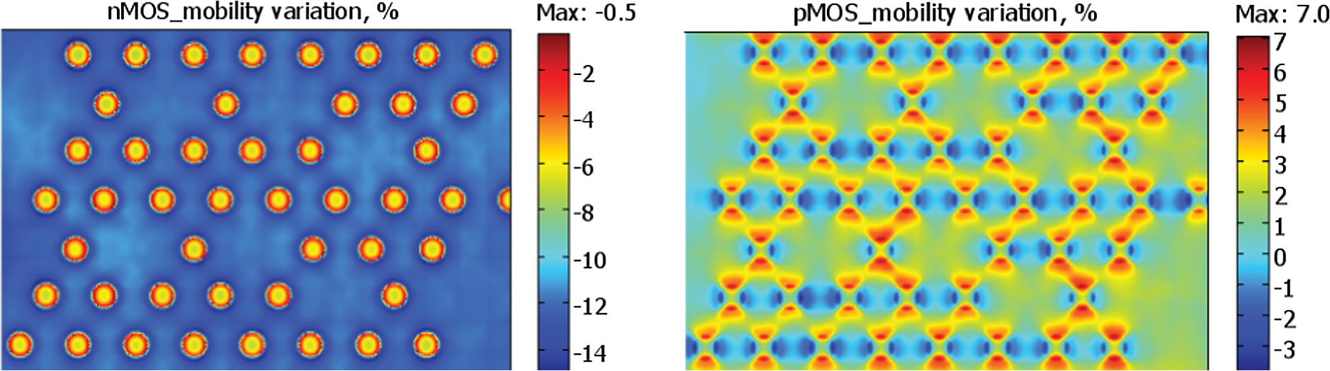
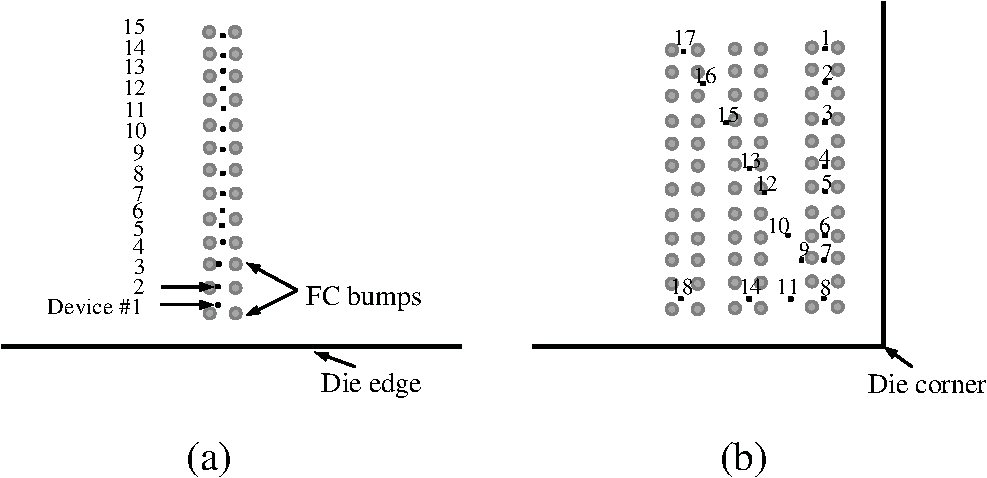
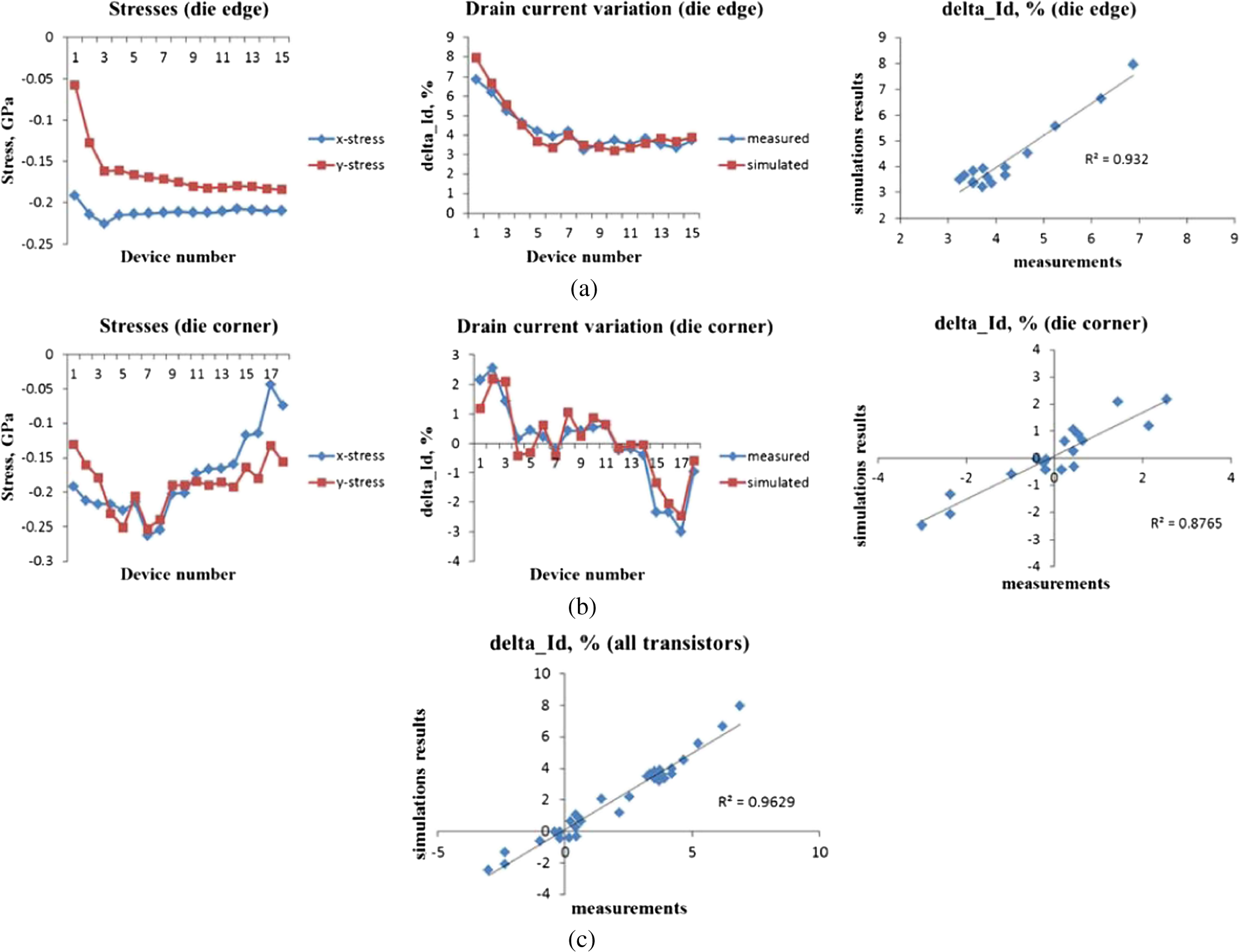
2.4.Compact Model for TSV-Induced StressTSV fabrication generates strain in the surrounding silicon: a thermal load generated by cooling the chip down from copper anneal temperature to room temperature creates a thermal mismatch strain due to large CTE difference between copper and silicon. The distribution of radial and circumferential stress components around the TSV, at a distance , where is the TSV diameter, can be approximated by Lame formula:14 Due to axial symmetry, the stress components of Eq. (7) in polar coordinates are independent of azimuthal angle . Equation (7) is valid when the TSV is placed far enough from the die periphery (at a distance much larger than ), where the boundary effects can be neglected. It should be mentioned that for more accurate description of TSV-induced stress distribution, the deformation of silicon surface due to prevailing vertical shrinking of the TSV in comparison with silicon should be considered.16 However, it can be shown that for the device layer, which is located very close to the silicon/BEoL interface, this surface effect results in just a renormalization of the parameter . In the discussed simulation flow, the value of this parameter should be determined by calibration. This should validate the employment of the Eq. (7) as an appropriate approximation for the effect of TSV on device characteristics. Vertical component of stress is essential only in the immediate vicinity of TSV and can be neglected since the devices are not allowed to be placed inside the so-called “keep-out-zones” around TSVs, where zone size is prescribed by the design rules. The radial and circumferential components [Eq. (7)] of TSV-induced stress can be transformed to the Cartesian components by This transformation provides These stress components should be determined in the same grid points, which were used for calculation of CPI stress components [Eq. (5)]. Finally, assuming that CPI and TSV stresses are independent and contribute additively, the total stress distribution is determined as 2.5.Simulation of the Transistor Intrachannel Stress ComponentsThe generated across-die distributions of stress components make it possible to calculate the averaged stress components inside transistor channels by using a simple interpolation procedure. However, at a device scale, the composite nature of the device layer becomes important. In fact, this layer represents a sequence of silicon islands separated by the shallow trench isolation (STI) regions filled by deposited silicon oxide. Keeping in mind a drastic difference in the mechanical characteristics of silicon and silicon oxide, as well as the fact that both the Si islands (i.e., the regions where the transistors are located) and STI regions are characterized by wide dispersion in sizes and shapes, we can conclude that strain distribution should depend on the local layout configurations of the device layer. FEA-based die-scale simulations of the CPI stress described in Sec. 2.3 cannot resolve the billions of shapes existing in devices layout. Therefore, in the next step of the multiscale simulation flow, a compact model-based calculation of the device-scale stress variations should be performed. This compact model considers the strain/stress distribution, calculated with Eq. (9), as an intial distribution that should be changed (relaxed) in accordance with the layout geometries. To calculate this stress redistribution, each transistor channel and the neighboring layout are portitioned on a set of “cut-layers” (both in - and -directions). Each cut-layer consists of the device layer and the silicon bulk, as shown in Fig. 6(a). The device layer consists of the sequence of segments representing slices of silicon islands and STIs separating silicon islands. Each ’th segment in the device “composite” layer is characterized by its length , Young’s modulus and Poisson’s ratio . The stresses given by Eq. (9) are considered as the “initial” stresses in each segment of the cutline. The difference in elastic properties of the neighbouring segments results in redistribution of this stress: each segment edge experiences additional lateral displacement due to the action of the forces . These displacements can be obtained from the solution of the force balance equation that takes into account the interaction between adjacent segments and the traction with the silicon bulk. Initial stress redistribution can be described as generation of an additional stress , which can be obtained from solution of the corresponding force balance equation. For example, for each cut-layer directed along -axis, the force balance equation for calculating the stress component is the following where is the shear stress component. Assuming that the vertical displacements everywhere in the plane are small in comparison with the lateral displacements, we can employ the following representation of stresses as functions of displacementsFig. 6Schematics of the cut-line: (a) vertical slice, (b) top view demonstrating device partitioning into cut-lines. Here, light polygons are silicon islands, narrow lines are the poly gates, small squares are contacts, and dark background is STI. 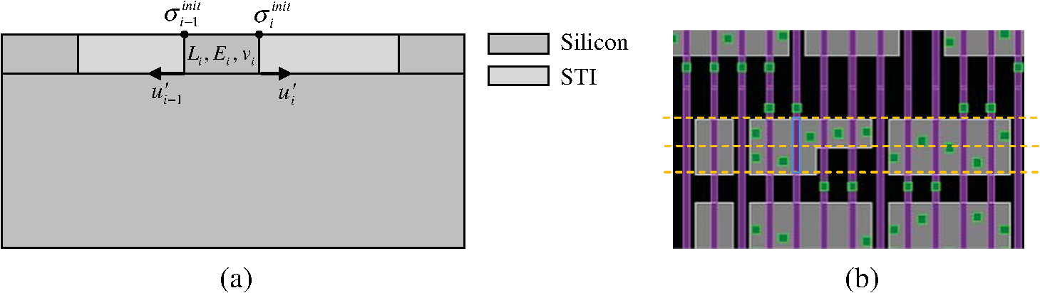 It reduces the problem to the solution of the following equation for the lateral displacement : As it was shown in Refs. 17 and 18, this equation can be further reduced to the system of linear equations for the lateral displacements at each node of the considered cut-line: Here, and are the Young’s modulus of ’th and ()’th segments; and are the known functions of the materials properties and segment geometries; is the initial strain in ’th node. These equations clearly demonstrate that the coupling between the global stress load (TSVs, packaging, bumps, etc.) and the resulted layout-induced stress distribution is introduced through the initial strain distribution calculated with the combined FEA-compact model. Solution of the system of Eq. (13) provides the distribution of displacements along all considered cut-lines, which after standard transformation [Eqs. (14) and (15)] generate the distribution of stress components everywhere in the cut-lines, and particularly inside the transistor channels, Fig. 6(b). 2.6.Stress-Induced Variation in Device Electrical CharacteristicsThe piezoresistive effect describes change in the electrical resistivity of a semiconductor or metal when mechanical strain is applied. In the case of semiconductors, this resistivity change is caused by the strain-induced modification of their band structure and results in mobility changes of the conductive electrons and holes. Stress-induced modification of the charge carrier mobility is calculated based on well-determined piezoresistance coefficients:19 Here, , is the low-field mobility in the stressed silicon, is the mobility at the zero stress condition;20 the signs and values of piezoresistance coefficients are known to be dependent on crystallographic orientation of silicon surface and on the transistor channel orientation.19,21 Correspondingly, for the SPICE instance parameter MULU0, we can write Figure 7 demonstrates the simulated mobility distributions in NMOS and PMOS transistors caused by an FC bump array for the case of channel direction. The magnitude of the mobility change depends on the pitch of bump pattern and on device location relative to bumps. SPICE netlist annotation with the calculated instant parameters MULU0 makes it possible to calculate stress-modified electrical characteristics of any device in the analyzed design by running SPICE simulator. It should be mentioned that the target of the developed simulation flow is the assessment of the effect of stresses associated with the 3-D IC technology on chip performance. These stresses are the unintentional and unwanted addition to the stresses already existing in the device layer generated by intentional stress sources, such as stressed layers (CESLs), source-drain epi-, stress memorization, etc., and unintentional ones (STI, residual, etc.). The total stress-induced variation of the transistor characteristics is caused by a combination of the layout-induced and package (CPI/TSV)-induced stresses. An instant parameter MULU0_layout describing the effect of the layout-induced stresses on the mobility can be calculated with the foundry calibrated SPICE models. A combined effect of these two types of stresses on the device characteristics can be obtained from SPICE simulations by employing the netlist annotated with MULU0 that represents the product of MULU0_layout and MULU0_3D. 3.Outline of the Calibration and Validation ProceduresFor calibration of the parameters involved into the developed compact models, the measured MOSFETs drain current should be used. Stress-induced variations of drain current are assumed to be caused by mobility variation, which is related to stress by means of relation.16 A representative set of transistors should be used for calibration, which means that the chosen transistors should be located on different distances from the die edges, corners, TSVs, and bumps. The drain current can be measured and simulated either in linear or in saturation regimes. As it was mentioned in the previous section, the 3-D stacking induced stress is not the only cause of variations. Layout-proximity effects (e.g., stress induced by built-in stressors, process/litho variations, wall-proximity effect, etc.) are able to introduce substantial variations of the device characteristics and should be treated properly. Therefore, the difference of the measured current , and the current calculated with the foundry calibrated SPICE model should be used for calibration: . The predicted values of the current variations caused by the 3-D stress in CMOS channels are related to the simulated stress components by the expression similar to Eq. (16): where the coefficients are related to piezoresistance coefficients by means of special transformation matrix that can be obtained by SPICE simulations.7 Then, the calibration engine tunes all the model parameters by minimizing the target function:The calibration results demonstrated below were obtained with the measurements done on a single-chip package where a 100-μm-thin silicon chip was mounted on the package substrate using FC bumps. Since this package did not contain TSVs, only the die warpage- and bump pressure-related effects were considered. The thicknesses and properties of the involved materials are listed in Tables 1 and 2. Figure 8 demonstrates the schematics of the structures used for the model calibration. They contain FC bump arrays located: Fig. 8(a) shows near the die edge and Fig. 8(b) shows near the die corner. MOSFET devices, located at different distances from FC bumps, were used for calibration. All these devices represent identical p-type transistors, having channel sizes. The identity of transistor sizes and the identical neighboring layouts have allowed us to exclude layout-induced variations in mobility, and thus to avoid the issues related to the accuracy of SPICE models of layout-proximity effects. The calibration results are demonstrated in Fig. 9. The relative changes of the drain current [i.e., ] for the selected p-type transistors are in the range of ~(3 to 7)% for the die-edge region, and for the die corner. These changes are caused by the demonstrated lateral stresses (having average values ). The effect of vertical stress component is much smaller due to small value of the corresponding piezoresistance coefficient: for the considered orientation of the channels the values of the piezoresistance coefficients are [in )]. The smaller values of the current variation in die corner region are due to higher values of -component of stress tensor, which reduces the current and for some transistors can surpass the positive effect of the -component. The obtained correlation between the measured and simulated values clearly demonstrates the calibration capability of the developed compact-model-based simulation flow. Fit of the model predictions to the measurements for all transistors, demonstrated in Fig. 9(c), is characterized by mean-square deviation of and maximal deviation of (in terms of relative change of the drain current). This corresponds to the stress prediction accuracy of . 4.Hot-Spot AnalysisDeveloped model, once calibrated with the test-chip data from a particular foundry and a technology node, can be employed for analyzing any design of the chips as long as the foundry manufacturing process and technology node are unchanged. It addresses the transistor-to-transistor variation of electrical characteristics caused by 3-D IC technology-induced stresses. However, full-chip detailed analysis of each transistor performance can be expensive in terms of time and CPU resources. So, it seems reasonable to have a capability of fast hot-spot analysis, or in other words, a capability for fast detecting the devices or circuits for which the CPI/TSV-induced stress impact can destroy the nets functionalities. Potential impact of the most stressed regions can be realized by means of the hot-spot analysis, consisting of the following steps:
5.ConclusionsThe paper describes the developed multiscale simulation methodology and flow for the assessment of the stress-induced performance variation in 3-D IC chips. The proposed approach allows the linkage between the package-scale FEA formats and the chip layout formats by means of the developed physics-based compact models. The accuracy of the stress prediction is enhanced by developing and implementing the compact models for the effective thermomechanical properties of the composite BEoL interconnect and BRDL layers. Finally, the compact model of the device-scale stress relaxation allows taking into account every individual transistor and its neighboring layout content. Depending on the design stage where the analysis is made, the simulation results can be used for hot-spot analysis, or for back annotating the SPICE netlist with instant parameter MULU0 allowing more accurate circuit simulations can be done. AcknowledgmentsThe authors would like to thank Drs. Riko Radojcic and Mark Nakamoto of Qualcomm for numerous target-oriented discussions. ReferencesR. RadojcicM. NowakM. Nakamoto,
“TechTuning: stress management for 3D through-Si-Via stacking technologies,”
in AIP Conf. Proc.,
5
–20
(2011). Google Scholar
G. Van der Plaset al.,
“Design issues and considerations for low-cost 3D TSV IC technology,”
IEEE J. Solid State Circuits, 46
(1), 293
–307
(2011). http://dx.doi.org/10.1109/JSSC.2010.2074070 IJSCBC 0018-9200 Google Scholar
S. Borkar,
“3D Integration for energy efficient system design,”
in Proc. IEEE Symp. VLSI Technology,
58
–59
(2009). Google Scholar
K. N. Tu,
“Reliability challenges in 3D IC packaging technology,”
Microelectron. Reliability, 51
(3), 517
–523
(2011). http://dx.doi.org/10.1016/j.microrel.2010.09.031 MCRLAS 0026-2714 Google Scholar
L. Mercadoet al.,
“Impact of flip-chip packaging on copper/low-k structures,”
IEEE Trans. Adv. Packag., 26
(4), 433
–440
(2003). http://dx.doi.org/10.1109/TADVP.2003.821084 ITAPFZ 1521-3323 Google Scholar
S. Flachowskyet al.,
“Understanding strain-induced drive-current enhancement in strained-silicon n-MOSFET and p-MOSFET,”
IEEE Trans. Electron Devices, 57
(6), 1343
–1354
(2010). http://dx.doi.org/10.1109/TED.2010.2046461 IETDAI 0018-9383 Google Scholar
K. Yamadaet al.,
“Layout-aware compact model of MOSFET characteristics variations induced by STI stress,”
IEICE Trans. Electron., E91-C
(7), 1142
–1150
(2008). http://dx.doi.org/10.1093/ietele/e91-c.7.1142 IELEEJ 0916-8524 Google Scholar
C.-Y. Chenget al.,
“New observations in LOD effect of 45-nm P-MOSFETs with strained SiGe source/drain and dummy gate,”
Trans. Electron Devices, 56
(8), 1618
–1623
(2009). http://dx.doi.org/10.1109/TED.2009.2022690 IETDAI 0018-9383 Google Scholar
E. Suhir,
“Predicted thermally induced stresses in, and the bow of, a circular substrate/thin-film structure,”
J. of Appl. Phys., 88
(5), 2363
–2370
(2000). http://dx.doi.org/10.1063/1.1286096 Google Scholar
E. Suhir,
“An approximate analysis of stresses in multilayer elastic thin films,”
ASME J. Appl. Mech., 55
(1), 143
–148
(1988). http://dx.doi.org/10.1115/1.3173620 JAMCAV 0021-8936 Google Scholar
S. M. Hu,
“Stress-related problems in silicon technology,”
J. Appl. Phys., 70
(6), R53
–R80
(1991). http://dx.doi.org/10.1063/1.349282 JAPIAU 0021-8979 Google Scholar
R. M. Jones, Mechanics of Composite Materials, Hemisphere Publishing Corporation, New York
(1975). Google Scholar
A. Ivankovicet al.,
“Thermo-mechanical impact of the Underfill-microbump interaction in 3D stacked integrated circuits,”
in IEEE 13th Electronic Packaging Technology Conf.,
34
–38
(2011). http://dx.doi.org/10.1109/EPTC.2011.6184506 Google Scholar
S. TimoshenkoJ. N. Goodier, Theory of Elasticity, McGraw-Hill, New York
(1952). Google Scholar
K. L. Johnson, Contact Mechanics, Cambridge University Press, UK
(1985). Google Scholar
S. K. Ryuet al.,
“Impact of near-surface thermal stresses on interfacial reliability of through-silicon-vias for 3-D interconnects,”
IEEE Trans. Device Mater. Reliab., 11
(1), 35
–43
(2011). http://dx.doi.org/10.1109/TDMR.2010.2068572 ITDMA2 1530-4388 Google Scholar
V. Sukharevet al.,
“3D IC TSV-based technology: stress assessment for chip performance,”
in AIP Conf. Proc.,
202
–213
(2010). http://dx.doi.org/10.1063/1.3527127 Google Scholar
V. Sukharevet al.,
“Multi-scale simulation methodology for stress assessment in 3D IC: effect of die stacking on device performance,”
J. Electron. Test., 28
(1), 63
–72
(2012). http://dx.doi.org/10.1007/s10836-011-5259-y JTTAER 0923-8174 Google Scholar
C. Smith,
“Piezoresistance effect in germanium and silicon,”
Phys. Rev., 94
(1), 42
–49
(1954). http://dx.doi.org/10.1103/PhysRev.94.42 PHRVAO 0031-899X Google Scholar
M. Dungaet al., BSIM4.6.0 MOSFET Model, University of California, Berkeley
(2006). Google Scholar
S. Thompsonet al.,
“Uniaxial-process induced strained-Si: extending the CMOS roadmap,”
IEEE Trans. Electron Devices, 53
(5), 1010
–1020
(2006). http://dx.doi.org/10.1109/TED.2006.872088 IETDAI 0018-9383 Google Scholar
BiographyArmen Kteyan received his MS degree in semiconductor physics and technology from Yerevan State University, Yerevan, Armenia, in 1994, and a PhD degree in solid state physics from the Institute of Radiophysics and Electronics (IRPhE) of Armenian National Academy of Sciences in 1998. The research activity at IRPhE was in the field of theory of dislocations in metals and semiconductors, and theory of superconductivity. Currently, he is a member of the technical research staff at Mentor Graphics and involved in development of physics-based models for DFM applications. Gevorg Gevorgyan received his MS degree in computer science in 2012 from the Yerevan State Engineering University, Yerevan, Armenia. Currently, he is an engineer in Mentor Graphics Corporation and is involved in software development for EDA applications. Henrik Hovsepyan received his MS degree in computer science from Yerevan State University, Yerevan, Armenia. He held senior technical positions at Ponte Solutions, Mountain View, California, working on physical design/verification, critical area analysis. Since 2008, he has been with Mentor Graphics Corporation, Fremont, California, as a part of the Ponte Solutions acquisition, where he was a lead engineer. His major research activity is related to the development of new full-chip modeling and simulation capabilities for the semiconductor processing and DFM applications. Jun-Ho Choy is an active staff engineer of Mentor Graphics Corp., Fremont, California. He received his BS degree at Seoul National University, his MS at Sung Kyun Kwan University, and his PhD at Michigan Technological University, Houghton, Houghton, MI, all in the field of metallurgical and materials engineering. He held the positions of device engineer in the Memory R&D Division at Hynix Semiconductor, Inc., and a principal engineer at LSI Logic Corp, Milpitas, California. Subsequently, he joined Ponte Solutions, Inc. (later acquired by Mentor Graphics), and participated in the development of full-chip DFM/DFR EDA tools. Valeriy Sukharev is a technical lead at the Design to Silicon Division of Mentor Graphics Corporation, Fremont, California. He leads research and development of new full-chip modeling and simulation capabilities for the semiconductor processing and DFM/ DFR applications. Prior to Mentor Graphics, he was a visiting professor with Brown University, Providence, Rhode Island, and a guest researcher with NIST, Gaithersburg, MD. He held senior technical positions at LSI Logic Advanced Development Lab, Milpitas, California. He holds a PhD in physical chemistry from the Russian Academy of Sciences. |