|
|
1.IntroductionThe directed self-assembly (DSA) has been considered as a viable option for next generation lithography. Some DSA patterning processes have already been investigated in a manufacturing environment, e.g., density multiplication of line (or hole) patterns,1 and hole shrink process.2 One of the remaining issues for these DSA processes is to reduce the defect level.3,4 According to the International Technology Roadmap for Semiconductors (ITRS), the defect level for the current DSA processes is still far from the manufacturing requirement.5 The DSA hole shrink process which we have investigated in this study is implemented as follows (Fig. 1).2 First, the guide holes (e.g., contact or via holes) are etched into the silicon-on-glass (SOG) and silicon-on-carbon (SOC) hardmasks, using conventional lithographic methods [Fig. 1(a)]. Then, an asymmetric poly(styrene-block-methylmethacrylate) diblock copolymer (PS-b-PMMA) is spin-coated and annealed on the etched wafer. Here, the minor block is PMMA and the major block is PS. After annealing, the PS-b-PMMA is phase-separated into the PS-rich and PMMA-rich domains, and the PMMA-rich domain is transformed into a vertical cylinder [Fig. 1(b)]. Note that the sidewalls and bottom surface of the guide hole are covered with a very thin layer of PMMA due to their higher affinity to the PMMA.2,6 The diameter of the cylindrical PMMA domain is typically on the order of to 30 nm, depending on the molecular weight of the PS-b-PMMA. After the selective removal of the cylindrical PMMA domain, the smaller hole is generated in the guide hole pattern. Fig. 1Directed self-assembly hole shrink process: (a–c) schematic process flow and (d) cross-sectional transmission electron microscopy (TEM) image after the removal of the cylindrical PMMA domain. In (d), the yellow line illustrates the outline of PS domain, the red arrow indicates the thickness of the bottom PS layer. 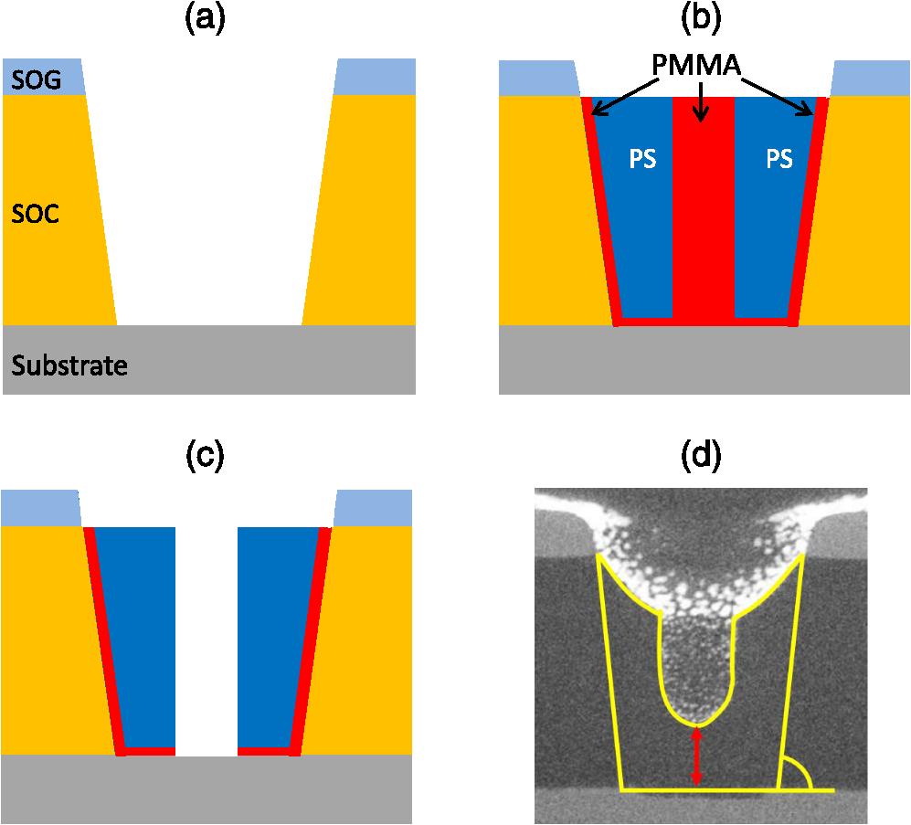 A crucial issue for the DSA hole shrink process is the morphological defects of the block copolymer generated during the annealing step.2,4 As shown in Fig. 1(d), the relatively thick PS layer remains between the cylindrical PMMA domain and the bottom surface. Depending on the thickness of the PS residual layer, it will be difficult to control the etching process which is followed by the DSA hole shrink process. It is also important to note that the PS residual layer is hardly detected by the conventional top-down scanning electron microscope (SEM) image. Simulation can be a powerful tool to predict the three-dimensional (3-D) morphology of PS-b-PMMA in the guide hole. Some simulation methods, such as dissipative particle dynamics (DPD)6,7 and self-consistent field theory (SCFT)8 have successfully demonstrated the formation of the cylindrical PMMA domain and the bottom PS layer with the sidewalls and bottom surface attractive to the PMMA. These simulation methods could also provide some useful insights into the chain conformation of the block copolymer, although they would be computationally expensive, particularly for the 3-D systems required for the DSA hole shrink process. In this study, we have employed a simplified model, called the Ohta–Kawasaki (OK) model9,10 to achieve a quick turnaround time for finding the optimal process condition for the DSA hole shrink process. In prior to the optimizations, we have calibrated the model parameters (i.e., interactive parameters between the walls of the guide hole and the blocks of PS-b-PMMA) with cross-section transmission electron microscopy (TEM) images. Taking advantage of the considerably small computational expense of the OK model, in the optimizations we have explored various guide hole shapes and minimized the thickness of the PS residual layer. This paper is organized as follows. Section 2 describes the details of the simplified model used in this study. Section 3 discusses our simulation results, including the comparison of the OK model with the SCFT (Sec. 3.1), calibration of the model parameters with the cross-sectional TEM images (Sec. 3.2), minimization of the thickness of the PS residual layers (Sec. 3.3), and the model extensibility to multiple cylinder cases (Sec. 3.4). 2.Model and Methods2.1.ModelIn this study, we employed the OK model described in Ref. 9. The free energy of the bulk diblock copolymer, , is expressed as where the coefficients, , , and , are the model parameters, and is the Green function (, : position vector). The order parameter, , is defined by , with as the volume fraction of the minor segments (i.e., PMMA). The average order parameter, , is calculated from , where is the fraction of the minor block per copolymer chain. Based on the OK’s phase diagram,9 the model parameters were selected as and , for which a stable cylindrical morphology was formed in the bulk at .The sidewalls and bottom surface of the guide are covered with a thin PMMA layer due to their higher affinity to the PMMA.2,6 In order to describe such attractive interactions between the walls and the PMMA, we added the following energy term where is the volume fraction of the PMMA in the vicinity of the walls. Equation (2) constrains the volume fraction of PMMA on the walls to be a constant, . The position-dependent coefficient, , was set at () on the walls, and 0 elsewhere. (Note that the Dirichlet boundary condition, i.e., at the walls, was not sufficient to reproduce the flat and thin layer of the PMMA on the walls.11)2.2.Simulation MethodsThe time-dependent Ginzberg–Landau equation was employed to obtain an equilibrated morphology of the PS-b-PMMA in the guide hole;10 where , , and are the time, diffusion constant, and chemical potential, respectively. The chemical potential, , was calculated fromEquation (4) was derived from the functional derivative of the system’s free energy with respect to the order parameter, i.e., . After substituting Eq. (4) into Eq. (3), the time evolution equation of the order parameter was given by withEquations (5) and (6) were numerically resolved with the same approach which was employed in our previous study:10
2.3.Experiments and Calibration DataThe DSA hole shrink process was implemented with the same process as described in Ref. 2. (1) The SOG and the SOC were deposited on the silicon with the thickness of 35 and 100 nm, respectively. (2) The holes were etched into the SOG and the SOC hardmasks. (3) The asymmetric PS-b-PMMA diblock copolymers (natural period , ) were spin-coated and annealed on the prepatterned substrate. (4) The cylindrical PMMA domain was formed at the center of the prepatterned hole and it was selectively removed by etching. (5) The inner hole was transferred to the substrate via plasma etching. The cross-sectional TEM images were taken after Step (2) to estimate the 3-D size of guiding holes. The top and bottom critical dimensions (CDs) were directly measured from the TEM images, and the taper angle was estimated from the two measured CDs (assuming that the SOC thickness is ). Next, the cross-sectional TEM images were also taken after Step (4), i.e., selective removal of the cylindrical PMMA domain, to measure the thicknesses of the PS residual layer and the SOC layer (Fig. 2). Due to shrinking and/or tilting, there was a mismatch between the measured and actual SOC thickness (); the PS residual thickness was scaled with a factor of (100 nm)/[the measured SOC thickness (nm)]. The measurement data is summarized in Table 1. Fig. 2Cross-sectional TEM images after the removal of the cylindrical PMMA domain: (a) Sample 1, (b) Sample 2, and (c) Sample 3. See Table 1 for their details. 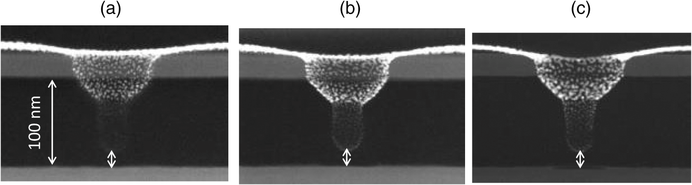 Table 1Guide hole shape and thickness of the PS residual layer measured/estimated from the cross-sectional TEM images in Fig. 2.
In addition to the thickness of the PS residual layer, the size of the cylindrical domain could also be measured from the cross-sectional TEM image and used as calibration metrics. However, due to some experimental uncertainties (e.g., shrinkage of the samples, change in size of the cylindrical domain before/after the removal of PMMA), it was not used for the calibration in this study. 3.Results and Discussions3.1.Three-Dimensional Morphology of PS-b-PMMA in Cylindrical Guide HoleAt first, morphology of the PS-b-PMMA in the cylindrical hole was simulated for several different hole diameters, . The detailed simulation conditions are summarized in Table 2. The lengths are scaled by the bulk native pitch of the cylindrical PMMA domain, . The surface parameters, and , were set at 100.0 and 0.7, respectively, with the sidewalls and bottom surface of the cylindrical hole PMMA being strongly attracted to the side and bottom walls. Table 2Simulation setup and calculation time used for the results in Fig. 3.
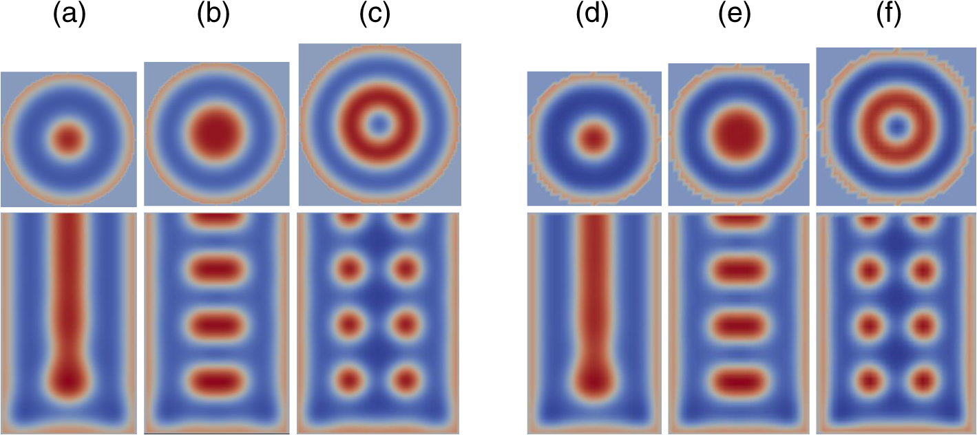
The simulation results are summarized in Fig. 3. At [], the cylindrical PMMA domain (red color) was formed at the center of the guide hole, whereas it was not in contact with the bottom surface due to the PS layer (blue). At [], the cylindrical PMMA domain was transformed to the horizontal disk-shape, then to a ring-shaped morphology. Similar morphological transformations were observed by the SCFT.8 It is still remarkable to see the formation of these nonbulk-like morphologies with the simplified model. It is also worth noting that each simulation was completed within 1 min (Table 2, bottom row). Such a short calculation time can be a large advantage over the other detailed models such as DPD and SCFT. Fig. 3Morphology of PS-b-PMMA in the guide hole simulated with the Ohta–Kawasaki model: (top) top-down view and (bottom) cross-sectional view. The PS-rich and PMMA-rich domains are shown in blue and red colors, respectively. The diameter of the guide hole is increased from (a) 1.59 [] to (k) 2.27 [], with the increment of []. 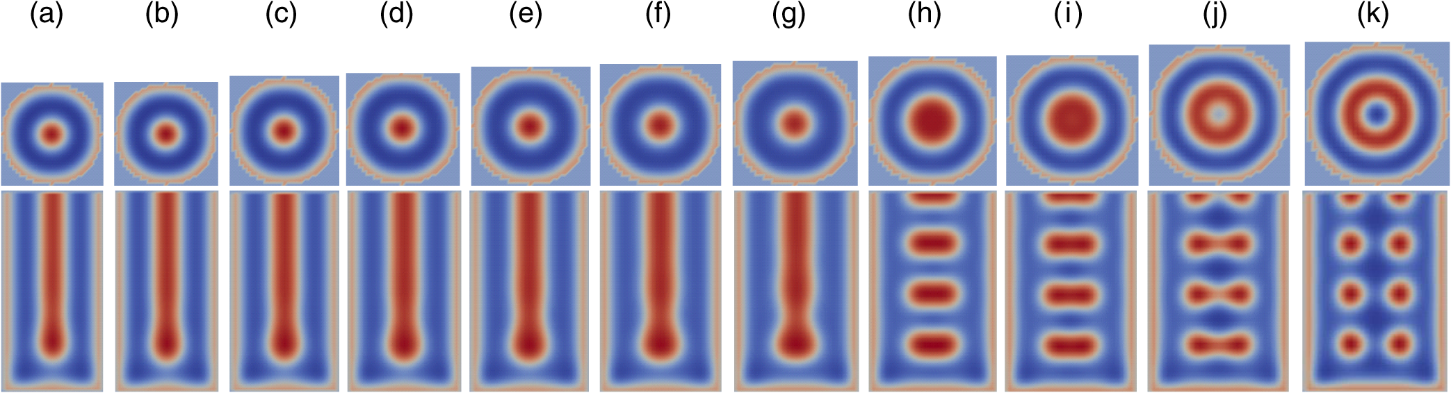 There were not any significant differences in the morphology observed by increasing the grid size (Fig. 4). It should also be noted that our numerical calculations were performed by the standard central difference method; the calculation time could be further decreased by selecting the other numerical methods (e.g., time-implicit method12). 3.2.Model CalibrationThe model calibration was implemented using the following steps. (1) The shape of the guide hole was set to be the same dimension as the cross-sectional TEM images (Table 1). (2) Simulations were performed with the OK model. (3) The thickness of the bottom PS layer was estimated for all three samples. (4) In order to reduce the errors between the simulated thickness and the experimental data (Table 1, bottom row), the two parameters in Eq. (2), and , were adjusted. First, was fixed at 100 (sufficiently large) and was changed from 0.5 to 1.0 (Fig. 5). As was decreased from 1.0, the errors were monotonically decreased. At , however, the simulated morphology of Sample 3 was no longer cylindrical (left inset of Fig. 5); the error became the smallest at . Next, was fixed at 0.6 and was varied from 10.0 to 200.0. It was found that the parameter, , had little effect on the shape of the cylindrical domain, but had a large effect on the shape and thickness of the PMMA layer on the bottom surface (Fig. 6). At , the PMMA layer on the bottom surface was undulating and touching the cylindrical PMMA domain (left inset of Fig. 6). As was increased from 10.0, the thickness of the PMMA layer was asymptotically decreased. We chose a sufficiently large value of () to stabilize the shape and thickness of the PMMA layer on the bottom surface. Fig. 5Model calibration with (). (a) Errors versus . The errors were estimated from the difference in the thickness of the bottom PS layer between the simulations and the experiments. The colors correspond to different samples: sample 1 (blue), sample 2 (red), and sample 3 (green). (b and c) The cross-sectional morphologies of sample 3 at and , respectively. 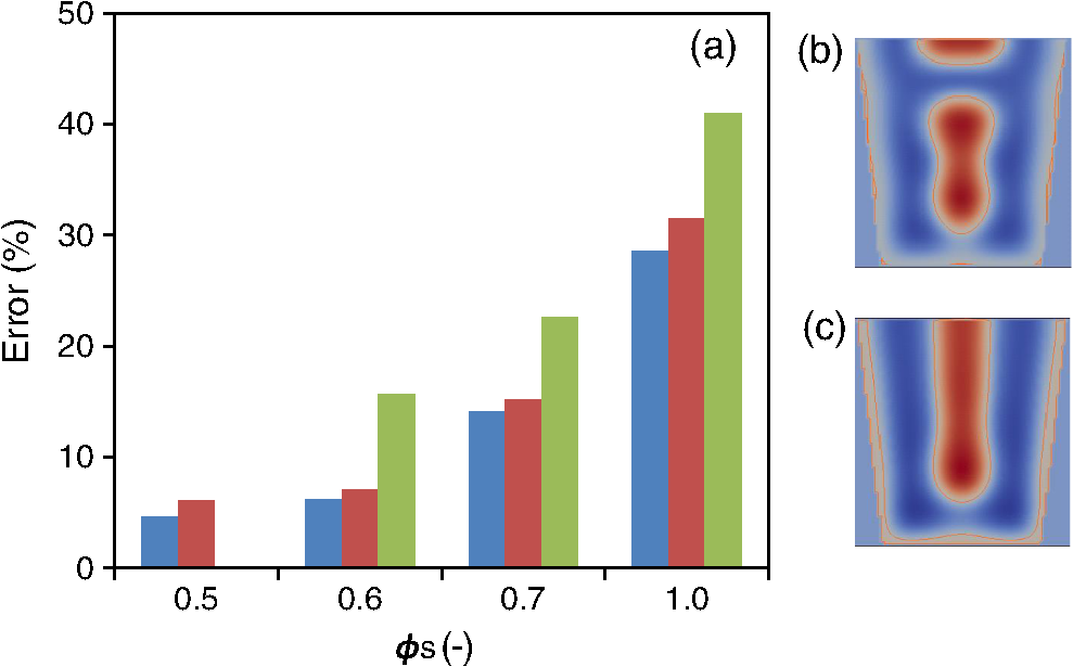 Fig. 6Model calibration with (). (a) Relationship between the parameter and the thickness of PMMA layer on the bottom surface. The colors correspond to different samples: sample 1 (blue), sample 2 (red), and sample 3 (green). (b and c) The cross-sectional morphologies of sample 1 at and , respectively. 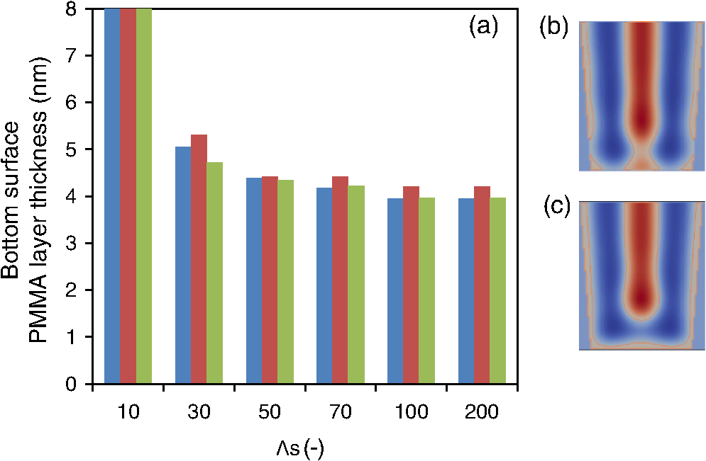 3.3.Guide Hole OptimizationIn order to decrease the thickness of the bottom PS layer, the shape of the guide hole was varied as follows: a taper angle from 84 to 90 (deg), a top CD from 1.6 to 2.1 [], and a depth hole from 1.8 to 2.2 []. The surface parameters were set to be the ones obtained from the model calibrations (i.e., and ). Figure 7 shows an example of the top CD effect on the morphology of the cylindrical PMMA domain and the bottom PS layer. The thickness of the bottom PS layer was gradually decreased as that of the top CD was increased. At the top [], the cylindrical PMMA morphology was broken into the two smaller domains. Figure 8 illustrates the contour plots of the thickness of the bottom PS layer at three different heights of the guide hole. The area where the thickness of the bottom PS layer is relatively small (shown in blue color) becomes slightly larger with a decrease in height of the guide hole. It should be noted that, even at the hole height of 1.8 [], the minimum thickness of the bottom PS layer is relatively large, []. It is difficult to reduce the thickness of the bottom PS layer by only varying the shape of the guide hole. Fig. 7Effect of the top CD on the morphology of PMMA-rich domain and the bottom PS layer. The taper angle and the hole height are fixed at 86 deg and 2.22 [], respectively. The top CD is increased from the left to the right: (a) 1.56, (b) 1.67, (c) 1.78, (d) 1.89, (e) 2.00, and (f) 2.11 []. 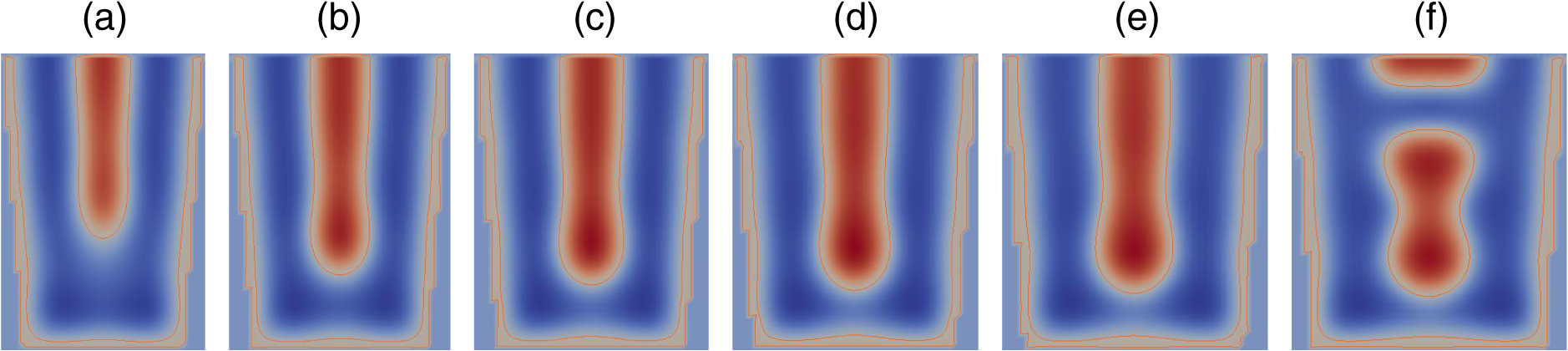 Fig. 8Contour plot of the thickness of the bottom PS layer with respect to the top CD (horizontal axis) and the taper angle (vertical axis). The three heights of the guide hole were examined: (a) 2.2, (b) 2.0, and (c) 1.8 []. The color represents the thickness of the bottom PS layer. 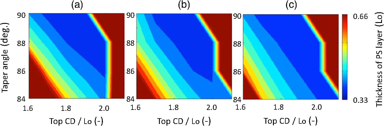 Next, the affinity of the bottom surface of the guide hole was modified from “PMMA attractive” to “neutral ().” As shown in Fig. 9, with the neutral bottom surface, the cylindrical PMMA was able to touch the substrate, i.e., no PS layer in between. A similar effect of the surface affinity on the cylindrical morphology was reported in Ref. 8, where the simulations were performed by the SCFT. Figure 10 illustrates the process window for the neutral bottom surface. It is clearly seen that the “no PS residual layer” region (dark blue color) can exist in a relatively wide range, e.g., a taper angle from 88 to 90 (deg) at the top [], or a top CD from to [] at a taper angle of 84 to 90 (deg). Fig. 9Effect of the affinity of the bottom surface on the morphology of the cylindrical PMMA domain: (a and c) PMMA-attractive, and (b and d) neutral bottom surface. The schematic cross-section of the guide hole is illustrated on the top, and the simulated morphology of the cylindrical PMMA domain (orange color) is shown on the bottom. 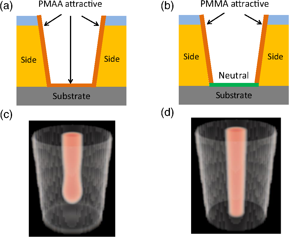 Fig. 10Contour plot of the thickness of the bottom PS layer with respect to the top CD (horizontal axis) and the taper angle (vertical axis), for the case of neutral bottom surface. The three heights of the guide hole were examined: (a) 2.2, (b) 2.0, and (c) 1.8 []. The color represents the thickness of the bottom PS layer. 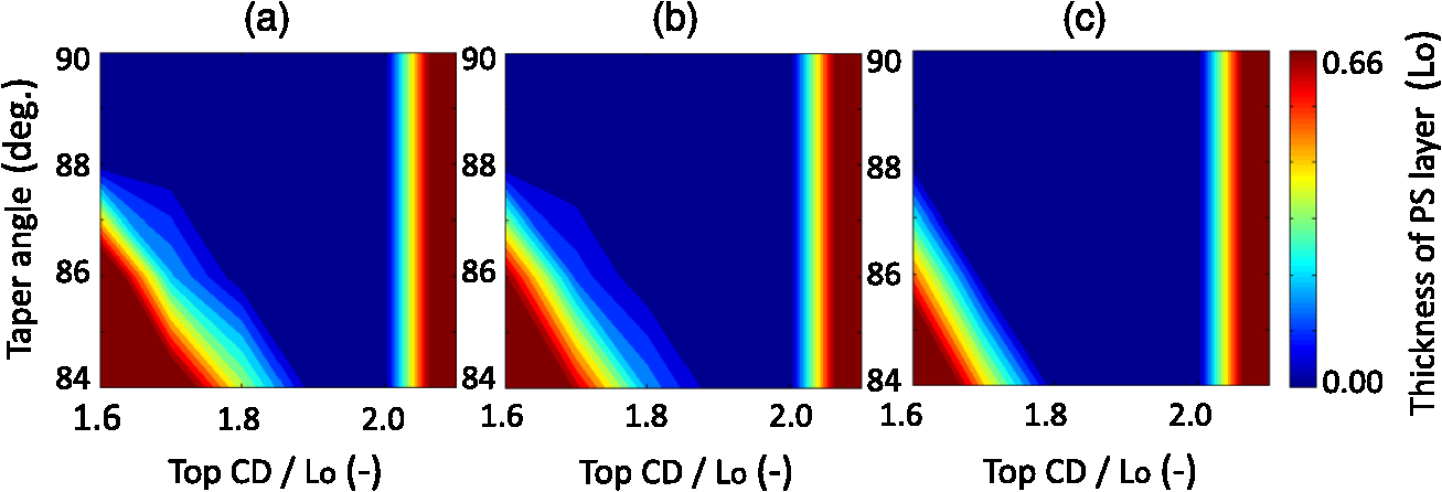 3.4.Model Extensibility to Multiple CylindersUsing exactly the same model parameters, we have also investigated the phase-separated morphology of PS-b-PMMA in the elliptical holes. In experiments, multiple cylindrical PMMA domains were observed in the elliptical holes (e.g., Ref. 13). Figure 11 illustrates a schematic design of the elliptical guide hole. The sidewalls and bottom surface of the elliptical guide hole were assumed to be attractive to PMMA. The height and the minor CD of the guide hole were fixed at 2.2 and 1.3 [], respectively. Only the major CD was changed from 2.0 to 4.0 [], with an increment of 0.22 []. Fig. 11Parametric setup of the elliptical guide hole: (a) top-down image and (b) cross-sectional views. 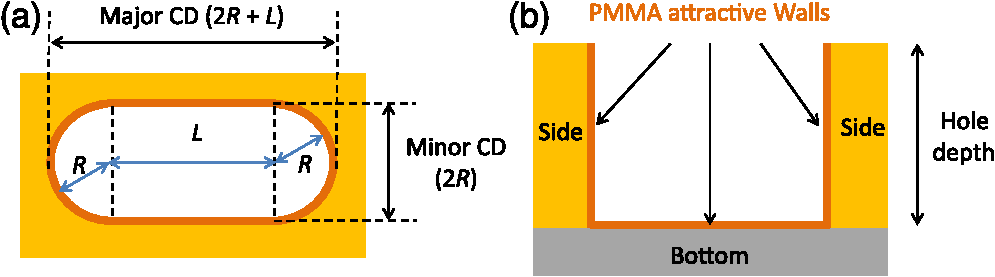 The simulation results are summarized in Fig. 12. The double cylinders were observed at a major CD of to 2.9 []. Interestingly, from the single to the double, and from the double to the triple, horizontal cylinders were formed. At the major CD of to 3.8 [], there were apparently triple cylindrical domains from the top view, but the two side ones were found to be connected via a horizontal cylindrical domain below the top surface. Such U-tube morphologies would be another type of defect, which could not be detected only by the top-down SEM images. In case the bottom surface was “neutral” instead of “PMMA attractive,” the morphological defects were eliminated and multiple cylindrical PMMA domains were in contact with the bottom surface (Fig. 13). Fig. 12Simulated phase-separated morphologies of PS-b-PMMA in the elliptical guiding hole: (top) top-down view, (middle) cross-sectional view, and (bottom) diagonal view of the simulated PMMA domain in the elliptical guide hole. The major CD is increased from (a) to (j), with the increment of 0.22 []. 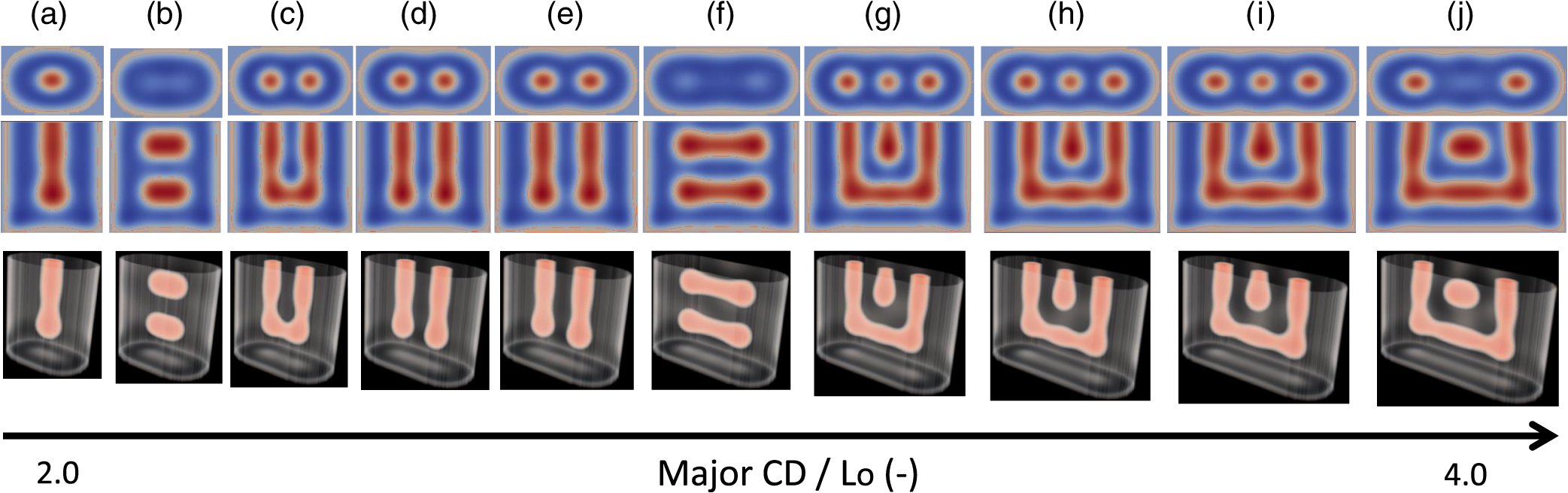 Fig. 13Effect of the neural bottom surface on the phase-separated morphologies of PS-b-PMMA in the elliptical guiding hole: (top) top-down view, (middle) cross-sectional view, and (bottom) diagonal view of the simulated PMMA domain in the elliptical guide hole. The major CD is increased from (a) to (j), with the increment of 0.22 []. 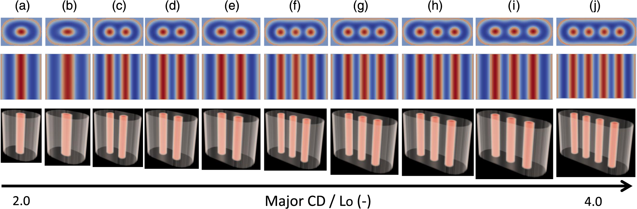 4.ConclusionsIn this study, we have applied the simplified model, called the Ohta–Kawasaki model, to find the optimal process conditions at which the thickness of the PS residual layer was minimized. Prior to the optimization, we demonstrated that the simplified model not only has a reasonable accuracy, but also an extremely short calculation time. Then, we calibrated the model parameters with the cross-sectional TEM images, and minimized the thickness of the PS residual layer by varying the guide hole shape (i.e., hole diameter, height, and taper angle). Our simulation results showed that it is difficult to eliminate the entire PS residual layer by only varying the guide hole shape. Alternatively, by changing the affinity of the bottom surface from “PMMA-attractive” to “neutral,” we could obtain a relatively wide, defect-free (i.e., no PS residual layer) process window. The same effect on the neutral bottom surface was observed for the case with an elliptical guide hole. Since our simulations are computationally inexpensive and scalable, they may also be feasible for large-scale simulations such as the hotspot (i.e., defects) analysis over a large area. AcknowledgmentsK. Y. and K. F. would like to acknowledge “Collaborative Research Program for Young Scientists of ACCMS and IIMC, Kyoto University,” for the use of the supercomputing facility. This research was partially supported by Japan Society of the Promotion of Science (JSPS) KAKENHI with the Grant Number 25900237. ReferencesR. Gronheidet al.,
“Readying directed self-assembly for patterning in semi-conductor manufacturing,”
J. Photopolym. Sci. Technol., 26
(6), 779
–791
(2013). http://dx.doi.org/10.2494/photopolymer.26.779 JSTEEW 0914-9244 Google Scholar
Y. Seinoet al.,
“Contact hole shrink process using graphoepitaxial directed self-assembly lithography,”
J. Micro/Nanolith. MEMS MOEMS., 12
(3), 033011
(2013). http://dx.doi.org/10.1117/1.JMM.12.3.033011 JMMMHG 1932-5150 Google Scholar
P. R. Delgadilloet al.,
“Defect source analysis of directed self-assembly process,”
J. Micro/Nanolith. MEMS MOEMS., 12
(3), 033112
(2013). http://dx.doi.org/10.1117/1.JMM.12.3.031112 JMMMHG 1932-5150 Google Scholar
C. Bencheret al.,
“Directed self-assembly defectivity assessment. Part II,”
Proc. SPIE, 8323 83230N
(2012). http://dx.doi.org/10.1117/12.917993 PSISDG 0277-786X Google Scholar
“The International Technology Roadmap for Semiconductors 2011 Ed. Lithography,”
http://www.itrs.net/Links/2011ITRS/2011Chapters/2011Lithography.pdf Google Scholar
K. Koderaet al.,
“Novel error mode analysis method for graphoepitaxial directed self-assembly lithography based on the dissipative particle dynamics method,”
Proc. SPIE, 8680 868015
(2013). http://dx.doi.org/10.1117/12.2011439 PSISDG 0277-786X Google Scholar
T. Nakanoet al.,
“Dissipative particle dynamics study on directed self-assembly in holes,”
Proc. SPIE, 8680 86801J
(2013). http://dx.doi.org/10.1117/12.2011069 PSISDG 0277-786X Google Scholar
N. Laachiet al.,
“The hole shrink problem: theoritical studies of directed self-assembly in cylindrical confinement,”
Proc. SPIE, 8680 868014
(2013). http://dx.doi.org/10.1117/12.2011198 PSISDG 0277-786X Google Scholar
K. YamadaM. NonomuraT. Ohta,
“Fddd structure in AB-type diblock copolymers,”
J. Phys.: Condens. Matter, 18
(32), L421
–L427
(2006). http://dx.doi.org/10.1088/0953-8984/18/32/L03 JCOMEL 0953-8984 Google Scholar
M. PinnaX. GuaoA. V. Zvelindovsky,
“Diblock copolymers in a cylindrical pore,”
J. Chem. Phys., 131
(21), 214902
(2009). http://dx.doi.org/10.1063/1.3264946 JCPSA6 0021-9606 Google Scholar
K. YoshimotoT. Taniguchi,
“Large-scale simulations of directed self-assembly with simplified model,”
J. Photopolym. Sci. Technol., 26
(6), 809
–816
(2013). http://dx.doi.org/10.2494/photopolymer.26.809 JSTEEW 0914-9244 Google Scholar
T. Uneyama,
“Density functional simulation of spontaneous formation of vesicle in block copolymer solutions,”
J. Chem. Phys., 126
(11), 114902
(2007). http://dx.doi.org/10.1063/1.2463426 JCPSA6 0021-9606 Google Scholar
R. Tironet al.,
“The potential of block copolymer’s directed self-assembly for contact hole shrink and contact multiplication,”
Proc. SPIE, 8680 868012
(2013). http://dx.doi.org/10.1117/12.2011477 PSISDG 0277-786X Google Scholar
BiographyKenji Yoshimoto is a project associate professor at the Center for the Promotion of Interdisciplinary Education and Research, Kyoto University, Japan. He received a BS degree from Kyoto University in 1999, and a PhD degree (major: chemical engineering) from the University of Wisconsin—Madison in 2005. His current research interests include modeling and simulations, polymer physics, and regenerative medicine. He is a member of SPIE. |