|
|
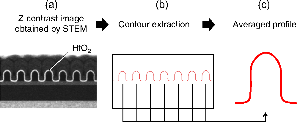
1.IntroductionThe impact of pattern-size deviation from the design value on the device performance is becoming more and more serious as large scale integration devices become more miniaturized.1 Even in cases where the average critical dimension (CD) is in the process margin, a slight variation in CD sometimes causes fatal degradation of device performance. In addition, the pattern edge roughness and deterioration of the two-dimensional pattern shape also can reduce production yield. Therefore, local measurements of patterns of several tens of nanometers are critical in advanced lithographic processing.2–4 Under these circumstances, the CD scanning electron microscope (CD-SEM) plays an important role in the inspection process during semiconductor manufacturing. As for the metrology of lithographic features, it is well known that photoresist (PR) materials shrink due to electron-beam (EB) irradiation during the acquisition of SEM images.5–7 The “linewidth slimming” caused by the SEM-induced shrinkage has been an issue because it causes an error in the CD measurements of PR patterns. This is especially serious in the case of ArF and most EUV photoresists because their base resins are sensitive to EB irradiation.7 Lowering the acceleration voltage and/or decreasing the irradiation dose density of the EB are effective ways to reduce the damage itself due to the EB irradiation.8–10 In addition, phenomenological methods for calculating the shrinkage amount of simple patterns, such as the lines and holes, have been developed.11,12 The original CD before SEM observation can be estimated using these methods, even though the shrinkage itself cannot be avoided. Nevertheless, confirmation that these methods for reducing or correcting the amount of shrinkage may be sufficiently effective for the more miniaturized patterns that will appear in future process nodes, or for those patterns with complicated shapes, is yet to be determined. The detailed mechanism of PR shrinkage should be clarified so that the shrinkage issue in future nodes can be overcome. Most studies on the mechanism of PR shrinkage have focused on the microscopic mechanism of the microscopic interaction between irradiated electrons and PR molecules.13–15 However, this microscopic interaction is a part of the shrinkage process. A change in the macroscopic pattern shape is important for practical purposes, such as reducing or correcting shrinkage. The following two points are essential in the macroscopic point of view. The first one is the distribution of incident electrons in the pattern, namely, the distribution of PR damage. The other is the effect of elastic deformation, namely, the pattern shape change induced as a result of the microscopic PR damage. Some recent studies on the distribution of incident electrons discuss that the electrons scattered from spaces around a given pattern into the pattern’s sidewall should be taken into consideration along with the directly-irradiated electrons.16–18 Some studies on the effect of elastic deformation mentioned its impact on the pattern shape change.19,20 Nevertheless, their experimental verifications were limited because they were based on measurements taken using an atomic force microscope (AFM) or a SEM. The shapes of the pattern’s foot are difficult to evaluate when taking AFM measurements because the AFM probe cannot access the angular foot region or the bottoms of dense patterns due to its tip size and tip rounding. In addition, pattern shrinkage is inevitable and three-dimensional (3-D) shape change is impossible to evaluate when taking SEM measurements. Therefore, a precise cross-sectional measurement method for PR line patterns is proposed in this paper based on this background. This method utilizes a scanning transmission electron microscope (STEM) after the atomic-layer deposition (ALD) of .21 The effect of the incident electron distribution and that of the elastic deformation are examined by comparing the change in the cross-sectional profile due to EB-irradiation under various conditions, such as accelerating voltages, irradiation doses and irradiated areas, together with the results from Monte Carlo simulations of the electron scattering in PR patterns. 2.Methods2.1.SamplesThe samples used for the STEM measurements included 45-nm half-pitch lines and spaces of ArF photoresists. We measured three samples with different material combinations, as shown in Fig. 1. They are positive tone developed (PTD) PR lines on a underlying layer, PTD PR lines on a bottom antireflective coating (BARC) underlying layer, and negative tone developed (NTD) PR lines on a underlying layer. The layers were spin-on-glass (SOG) layers which were fabricated by spin-coating of the mixture of and organic solvent. Hereafter, these three samples are referred to as the PTD/SOG sample, PTD/BARC sample, and NTD/SOG sample. Fig. 1Examples of top-down scanning electron microscope (SEM) images of (a) positive tone developed (PTD) photoresist (PR) lines on spin-on-glass (SOG) underlying layer (PTD/SOG sample), (b) PTD PR lines on bottom antireflective coating underlying layer (PTD/BARC sample), and (c) negative tone developed PR lines on SOG underlying layer (NTD/SOG sample). 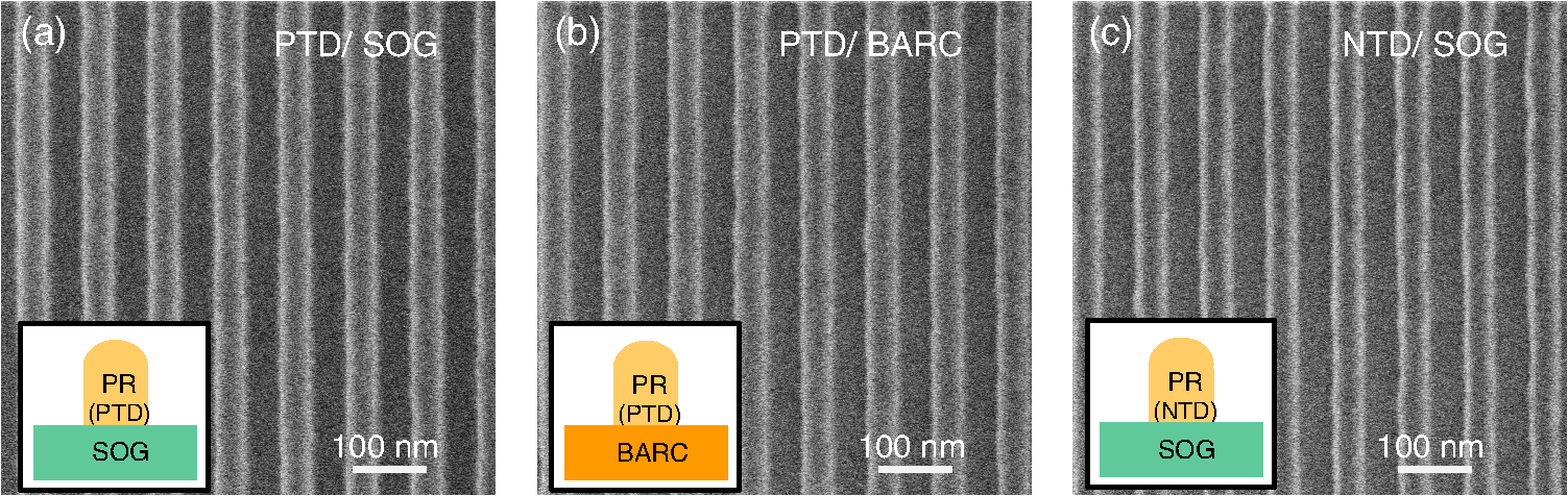 The elastic deformation of the PR patterns associated with BARC shrinkage can be examined because SOG is more rigid than BARC and is expected to be more durable against EB irradiation. In addition, since the pristine profile would be more angular for the NTD/SOG sample than for the PTD/SOG sample, the elastic deformation effect would be different between these two samples. 2.2.Scanning Transmission Electron Microscope MeasurementsThe process flow of the proposed cross-sectional measurement on EB induced PR-pattern shrinkage is shown in Fig. 2. First, a SEM is used to irradiate the EB on part of the PR line patterns to intentionally cause shrinkage. This SEM EB irradiation is denoted simply as “EB irradiation” hereafter. This does not mean the EB irradiation during the STEM observation performed afterward. Second, ALD is used to deposit a 2-nm thick thin film on the sample. The sample surface is thus conformally coated with a thin film. In the process, tetrakis(ethlmetylamino)hafnium and were used as precursors, the number of cycles was 14 and the process temperature was 80°C. Third, the sample is coated with amorphous carbon and tungsten layers to prevent pattern collapse during the following focused ion beam (FIB) process. Also during the process, the temperature was kept below 80°C in order to avoid thermal damage to the PR patterns. Fourth, a thin-film sample for the STEM observation is cut out by using a microsampling technique with a FIB. Finally, a cross-sectional Z-contrast image of the patterns is obtained by using a STEM with a 200-kV accelerating voltage. The thin film improves the Z-contrast at the pattern edge. As a result, the cross-sectional feature with a bright thin band, which corresponds to the PR pattern surface, is clearly shown in the image. The contour of the pattern is defined as the center of the bright thin band to further quantitatively evaluate the pattern shape. Fig. 2Process flow of cross-sectional measurement: (a) electron-beam (EB) irradiation on part of PR sample using SEM; (b) thin-film deposition; (c) coating with amorphous carbon and tungsten; (d) microsampling using focused ion beam; and (e) scanning transmission electron microscope (STEM) observation. 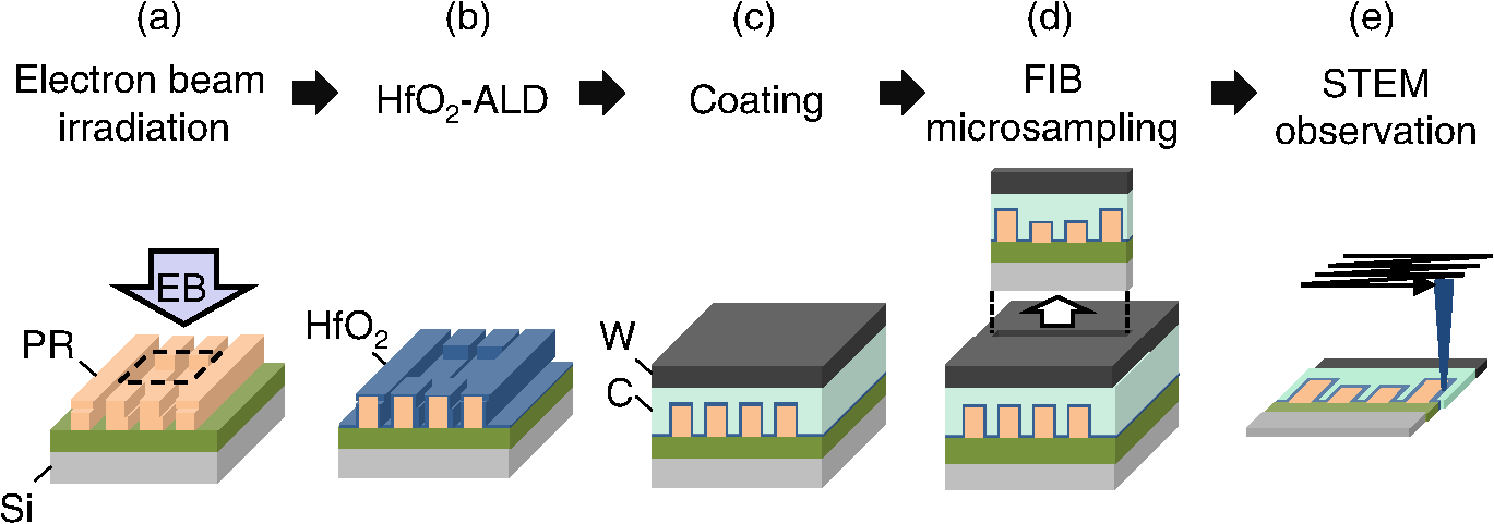 We confirmed that the above described sample preparation itself barely influences the measurement accuracy of the resist pattern profiles. An isolated PR line was measured using 3-D AFM22 before and after the ALD process. Figure 3(a) shows the obtained AFM cross-sectional profiles. The bold and dashed lines are the profiles obtained before and after the ALD process. Figure 3(b) shows the distance, or residuals, between these two profiles, which was plotted as a function of the position measured along the profile. The distance is about 2 nm except for the pattern’s foot region. This indicates that the 2-nm film was conformally deposited onto the resist surface and that the pattern shape was conserved during the ALD process. Dispersion of the distance, which is the nonuniformity of the ALD thickness, is larger in the pattern’s foot region, but is 2 nm at most. Considering that the profile is defined at the center of the bright band of the film, we can thus conclude that the profile error induced in the ALD process is at most 1 nm. Moreover, the obtained images do not change during a continuous STEM observation for more than 10 min. These results suggest the EB-induced damage formed during the STEM observation is negligible. This seems against the expectation that irradiation with the higher acceleration voltage causes the more serious shrinkage. It can be considered as an effect of a thin-film specimen. Qualitatively, such high-energy electrons have a rather small scattering cross section so that they possibly lead to almost no interaction event in a very thin film. For a quantitative confirmation, detailed experiments and simulations are needed that consider a film much thinner than a mean free path of the electrons. Fig. 3(a) Profiles measured by three-dimensional atomic force microscope before and after atomic-layer deposition (ALD) process. (b) Distance between profiles as function of position on profile before ALD process measured along the profile. The distance is almost constant, which confirms that the ALD film was conformally deposited and the pattern shape was conserved during the ALD process. The profile error due to the ALD process was 1 nm at most because the center of the ALD film was extracted as a profile. 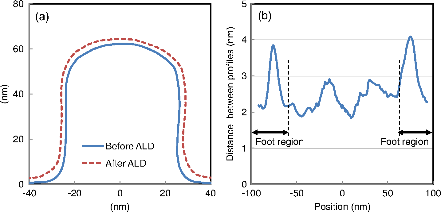 An averaging approach was adopted to reduce the local pattern-shape variation in order to evaluate the change in the cross-sectional shape due to shrinkage. Since a STEM measurement is a destructive one, it is impossible to compare the cross-sectional profiles of the same pattern before and after the shrinkage. The shrinkage is instead evaluated from a comparison of the results from different patterns in a same matrix of lines and spaces, effectively averaging the results of multiple but nominally equivalent cross-sections to suppress error due to roughness and finite local CD uniformity of the features under study. The procedure for averaging the profiles is shown in Fig. 4. A continuous contour was extracted from the bright thin band in the Z-contrast STEM image. The one contour obtained, which consists of multiple line pattern profiles, is divided into discrete profiles that correspond to each line. Then the profiles are aligned, folded and averaged. 2.3.Electron-Beam Irradiation ConditionsWe performed three series of STEM measurements under different SEM EB irradiation conditions to control the shrinkage shown in Fig. 2(a). A summary of the conditions is given in Table 1. Table 1Scanning electron microscope electron-beam irradiation conditions.
The first series was the measurement using dose-dependent irradiations. All three samples were evaluated in this examination. The EB accelerating voltage was 500 V, the irradiation area was , the number of pixels was 512 pix, and the dose density was varied from 0 to . This dose density of corresponds to 64 times the SEM image acquisitions using an 8-pA probe current. The second series was the measurement using area-restricted irradiations. The PTD/SOG sample was used and the EB irradiation area was restricted to a very narrow region at the center of the line patterns or spaces, as shown in the painted part of Fig. 5. Each narrow scan area was 22-nm wide and 675-nm long. The dose density was fixed at . This measurement was taken to clarify the effect of the scattered electrons from the spaces around the patterns. Fig. 5Schematic view of area-restricted EB-irradiation, where painted regions are irradiated areas. The lower diagram is a cross-section of the PR sample and the irradiated area.  The last series was the measurement using accelerating voltage dependent irradiations. The PTD/SOG sample was evaluated. The EB accelerating voltages were 100 and 500 V, and the dose densities were 0.2 and 1.6 nm. The irradiation area was fixed at 675 nm square. This measurement was taken to clarify the effect of the electron’s penetration depth, which depends on the accelerating voltage. 2.4.Electron Scattering SimulationElectron scattering simulations were conducted to obtain the spatial distribution of the energy transferred from the incident electrons to the PR patterns. A Monte Carlo simulator, Chariot,23 was used to calculate the trajectories and the energy loss of the incident electrons. In the Chariot simulations, the EB conditions were set to be equivalent to those of the experiments of area-restricted irradiations. The accelerating voltage of the incident electrons was 500 V. The irradiated region was 22-nm wide and located at the center of the lines or the center of the spaces. The incident dose was . The Mott model and the discrete loose approximation model were selected for the models describing elastic and inelastic scattering. Regarding the materials, polymethyl methacrylate () and were used to represent the PR and SOG. 3.Results and Discussion3.1.Result of Dose-Dependent IrradiationsFigure 6 shows cross-sectional STEM images for various EB preirradiation doses for all three samples. Each image contains the region with and without EB irradiation. These images show that the change in the cross-sectional shape due to the EB irradiation was clearly captured. The average cross-sectional profiles extracted from these STEM images are shown in Fig. 7, where the height origin (0 nm) is set to the bottom level of the nonirradiated region. This figure shows the detailed profile change, including the rapid shrinkage for a small dose, and how it slows down for a large dose, indicating the expected saturating tendency of the shrinkage (as observed in typical CD-SEM shrinkage measurements). Fig. 6Examples of acquired cross-sectional STEM images of: (a) PTD/SOG sample, (b) PTD/BARC sample, and (c) NTD/SPG sample. 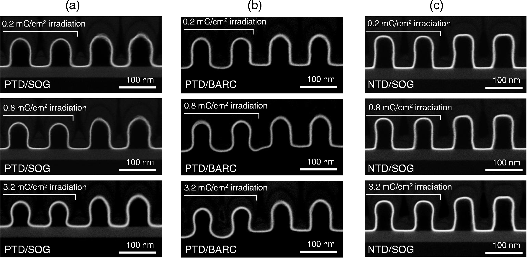 Fig. 7Extracted profiles of: (a) PTD/SOG sample, (b) PTD/BARC sample, and (C) NTD/SPG sample. Three interesting features associated with PR shrinkage were identified: the rounding of the top of the patterns, the regression of the BARC layer, and a necking profile in the pattern shape, namely, the maximum sidewall recession at the middle height. 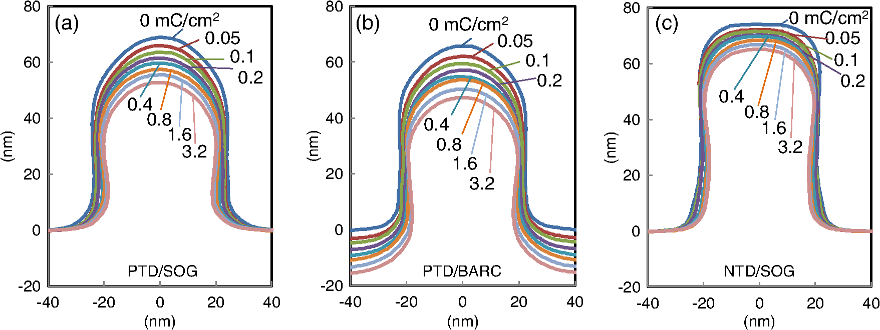 Three interesting features associated with the PR shrinkage can be identified from these results: the rounding of the top of the patterns, the regression of the BARC layer, and the necking profile in the pattern shape, namely, the maximum sidewall recession at the middle height. The top rounding feature was commonly observed for all three samples. The pattern top was similarly round-shaped after sufficient shrinkage, even though the NTD/SOG and PTD/SOG samples have quite different pristine cross-sectional profiles. The comparison of the results of these two samples clearly showed that the protuberant region, which is the pattern center for the PTD/SOG sample and the pattern’s shoulder for the NTD/SOG sample, retreated due to the compressive stress induced by the shrinkage. This is evidence of the elastic effects in shrinkage. The results from the PTD/BARC sample served as further evidence of the elastic effects. This sample showed a rounding of the foot region associated with the regression of the BARC layer. This behavior can be interpreted as follows. The foot region of the line patterns was pulled toward the outside oblique direction by the tensile stress induced by the underlying material in the spaces. The necking profile is rather complicated to interpret. This feature cannot be described in terms of elasticity. This issue will be discussed in Sec. 3.2 by referring to the results from the area-restricted irradiations and the Monte Carlo simulations. 3.2.Area-Restricted IrradiationsFigure 8 shows the cross-sectional STEM images and cross-sectional profiles of the PTD/SOG sample with the area-restricted EB irradiations. Figures 8(a) and 8(c) clearly show that the EB irradiation on the top of the PR line patterns causes a significant decrease in height and that there is no necking profile. On the other hand, Figs. 8(b) and 8(d) show that the EB irradiation only on the space region causes less height shrinkage and measurable sidewall recession and a necking profile. These contrasting behaviors suggest that the shrinkage processes in the pattern top and sidewall are different. The pattern-top shrinkage is mainly caused by the direct irradiation onto the pattern top. On the other hand, the sidewall shrinkage, including the necking profile, at least to some extent is caused by the electrons scattered from the spaces. This observation is consistent with the models presented elsewhere.17 Fig. 8(a) and (b) Acquired cross-sectional STEM images. The EB-preirradiated areas are indicated by arrows. (c) and (d) Extracted profiles for EB irradiation only on tops of patterns and only on spaces between patterns, respectively. The dashed lines are the pristine profiles. The EB irradiation on the top region causes a significant decrease in the height. On the other hand, the EB irradiation on the spaces causes a measureable sidewall shrinkage recession and a necking of the profile. 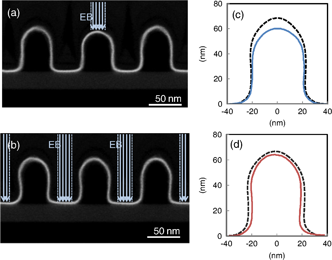 Figure 9 shows further evidence of the impact of the scattered electrons on the shrinkage phenomena. This is a STEM image of the PTD/SOG sample with the EB irradiated onto one side of the adjacent spaces, as shown by the arrows in the figure. The PR line patterns look as if they are leaning toward the irradiated side. In other words, the profile of the irradiated side shows a necking profile. This result clearly indicates that the sidewalls’ shrinkage and the necking profile stem from the scattered electrons. Fig. 9Acquired cross-sectional STEM image of area-restricted irradiations. The EB-irradiated areas are indicated by the arrows. The PR line patterns look as if they are leaning toward the irradiated side due to the shrinkage. 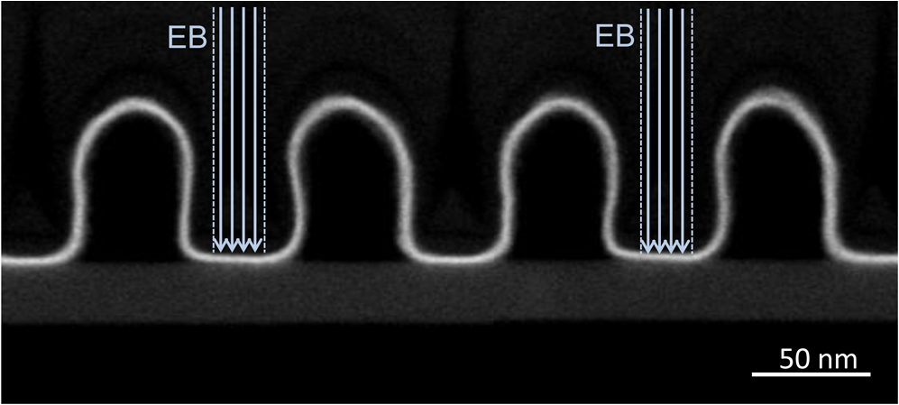 Figures 10(a) and 10(b) show the results of the electron scattering simulations for the area-restricted EB irradiation. The calculated energy distribution deposited on the PR lines was mapped using the experimentally obtained profiles before and after EB irradiation. In this calculation, all of the electrons were taken into account, including the secondary electrons (SEs) and back-scattered electrons (BSEs) from the spaces around the patterns. For the irradiation on the top, almost all the incident energy is deposited on the vicinity of the irradiated area at the top. Meanwhile, for the irradiation on the spaces, measurable energy is deposited on the sidewall via the scattered electrons. These results indicate that the height shrinkage in the SEM observation is mainly caused by the direct irradiation on the top of the pattern and that the electrons scattered from the spaces onto the sidewall contribute to the sidewall shrinkage. Quantitatively, the energy deposition density per unit surface area of the sidewall is about 5% of that on the top region in the case of irradiation on the top. Fig. 10Calculated distributions of energy deposition caused by EB irradiations on: (a) top of PR lines and (b) spaces between lines. The solid lines are the measured pristine profiles and the dashed lines are the measured profiles after shrinkage. (c) Height dependence of total energy deposition density on sidewall for EB irradiation on spaces. 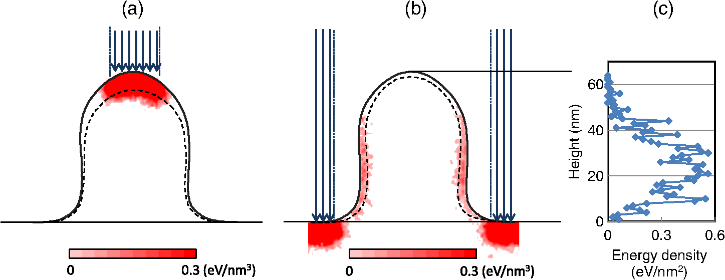 Figure 10(c) shows the height dependence of the energy-deposition density per unit surface of the sidewall for the irradiation on the spaces. The region with large energy deposition was found to be coincident with the necking location region (which was observed at around 20 nm above the bottom). It is, therefore, confirmed that the electrons scattered from the spaces cause the necking profile. 3.3.Electron-Beam Accelerating Voltage Dependent IrradiationsFigure 11 shows the averaged cross-sectional profiles of the PTD/SOG sample after EB irradiation using 100- and 500-V accelerating voltages with small and large doses. Fig. 11Extracted profiles of the PTD/SOG sample with 100 V and 500 V preirradiation (solid lines) shown together with the profiles without EB preirradiation (dashed lines): (a) small irradiation case and (b) large irradiation case. The difference of the shrinkage between 100 V case and 500 V is specifically small for the sidewall at large dose. It suggests that major cause of the sidewall shrinkage is the SEs emitted from the spaces because penetration depth of SEs is irrespective to the energy of incident electrons in contrast to that of back-scattered electrons. 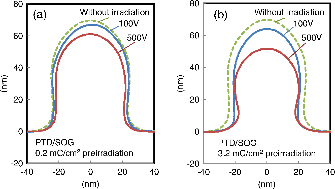 The decrease in height and the sidewall recession are much smaller for the 100-V EB-irradiation than for the 500-V EB-irradiation for a small dose, as shown in Fig 11(a). This is well expected from a naive description that states that an EB with a higher energy causes larger shrinkage. For a large dose, however, the sidewall recession is almost equivalent at both 100 and 500 V, although the decrease in height is still smaller for 100 V. This anomalous behavior can be interpreted by considering the difference in nature of the electrons inducing the shrinkage. Discussion in Sec. 2.2 revealed that the sidewall recession is mainly induced by the scattered electrons from the spaces, as reported in the literature.17 In the literature, it was regarded that the BSEs are the major cause of the sidewall recession because the energy of BSEs is much higher than the SEs. However, the observed equivalent sidewall recession does not meet this interpretation because the energy of BSEs is higher and the expected shrinkage is larger for the 500-V EB irradiation than for the 100-V EB-irradiation. On the other hand, the observed phenomenon can be interpreted by considering the SEs as the major cause of sidewall recession. The shrinkage amount should be controlled by the penetration depth of the incident electrons with an EB dose large enough for the saturation of shrinkage. Because the typical energy of SEs is universally several tens of eV, the typical penetration depth of SEs is generally irrespective of the incident EB energy. Thus, a similar amount of sidewall recession between the 100-V and the 500-V EB irradiations can be explained by the effect of SEs emitted from the spaces. Based on this interpretation, the result of the sidewall recession for a small dose implies that the dose of the SEs emitted from the spaces is larger for the 500-V case. This means that the SE yield of the SOG is larger for a 500-V EB irradiation than for a 100 V one. Although the SE yield of is difficult to determine by experiment due to charging, a simulation study which eliminates charging effect reported that the yield is larger for 500 V than for 100 V.24 Detailed investigations on the SE yield of are needed for a comprehensive interpretation of the observed accelerating-voltage dependency. 4.SummaryThe mechanism of the PR shrinkage induced by EB irradiation was studied. In particular, the change in the cross-sectional profile of the PR lines due to shrinkage was investigated in detail. Precise cross-sectional profiles were acquired by using a STEM with an ALD of film on the pattern surface. In the Z-contrast images, the film appeared as a bright band that can be considered as the cross-sectional profile. It was confirmed by an AFM reference measurement that the pattern shape was conserved during the ALD process at a profile error of less than 1 nm. This method was applied to the PR lines irradiated by EB under various conditions. The results of the measurements clearly revealed a detailed change in the cross-sectional profile due to the EB-induced shrinkage. This suggests that ALD and STEM are very powerful tools for the cross-sectional measurement of PR patterns. With these measured profiles, we experimentally clarified two important behaviors affecting the shrinkage. One is that the pattern shape is elastically deformed as a result of the shrinkage. For all the measured PR samples, a rounding of the top of the patterns appeared with the EB irradiation. This behavior can be interpreted as the result of the elastic deformation due to shrinkage. The rounding of the foot region accompanying the recession of the BARC layer observed for the PTD/BARC sample cannot be explained without also considering the elastic deformation. The other one is that the electrons arriving from the spaces around the patterns affect the sidewall shrinkage, as proposed in the literature.17 Moreover, we revealed that the SEs emitted from the spaces are the major cause of the sidewall shrinkage. We also found that the sidewall shrinkage was not a simple recession. The pattern width decreased most at the middle height, which appeared as a necking of the profile. Such sidewall recession accompanied with a necking profile was found to be generated by the EB irradiation only onto the spaces between the lines, and this is suggested to be caused by the electrons scattered in the spaces between the PR lines and entering into the sidewall. The results from a Monte Carlo simulation of the electron scattering showed the deposited energy distribution of the sidewall with a peak at the middle height, which is consistent with the necking profile. The results from the accelerating-voltage dependence experiments also can be interpreted by considering the difference in the electrons inducing shrinkage, which are the primary electrons in the top region and the SEs emitted from the spaces on the sidewall of the pattern. Consequently, we experimentally clarified two important effects to describe the shrinkage-induced shape change of the PR patterns. One is the elastic deformation effects. The other is the electron distribution in the pattern including the electrons scattered in the spaces around the pattern. The precise correction and effective reduction of the shrinkage can be achieved by taking these effects into consideration. AcknowledgmentsThe authors would like to thank M. Hori, M. Shimizu, and M. Shima of JSR Corporation for providing the PTD photoresist samples. References
“International Technology Roadmap for Semiconductors 2013 Edition,”
(2013). http://www.itrs.net/ Google Scholar
A. Yamaguchi et al.,
“Impact of long-period line-edge roughness (LER) on accuracy in critical dimension (CD) measurement and new guideline for CD metrology,”
Jpn. J. Appl. Phys., 44 5575
(2005). http://dx.doi.org/10.1143/JJAP.44.5575 Google Scholar
J. Sturtevant and E. Tejnil,
“Roadmap to sub-nanometer OPC model accuracy,”
Proc. SPIE, 8441 94410H
(2012). http://dx.doi.org/10.1117/12.978190 PSISDG 0277-786X Google Scholar
D. Hibino et al.,
“High-accuracy optical proximity correction modeling using advance critical dimension scanning electron microscope-based contours in next-generation lithography,”
J. Micro/Nanolith. MEMS MOEMS, 10 013012
(2011). http://dx.doi.org/10.1117/1.3530082 Google Scholar
T. Kudo et al.,
“CD changes of 193-nm resists during SEM measurement,”
Proc. SPIE, 4345 179
–189
(2001). http://dx.doi.org/10.1117/12.436847 PSISDG 0277-786X Google Scholar
C. Wu et al.,
“Investigation on the mechanism of the 193-nm resist linewidth reduction during the SEM measurement,”
Proc. SPIE, 4345 190
–199
(2001). http://dx.doi.org/10.1117/12.436848 PSISDG 0277-786X Google Scholar
T. Sarubbi et al.,
“Mechanism studies of scanning electron microscope measurement effects on 193-nm photoresists and the development of improved line-width measurement methods,”
Proc. SPIE, 4345 211
–221
(2001). http://dx.doi.org/10.1117/12.436837 PSISDG 0277-786X Google Scholar
G. Sundaram et al.,
“Low-impact resist metrology: the use of ultralow voltage for high-accuracy performance,”
Proc. SPIE, 5375 675
–685
(2004). http://dx.doi.org/10.1117/12.539221 PSISDG 0277-786X Google Scholar
H. Marchman et al.,
“Electron beam based modification of lithographic materials and the impact on critical dimensional metrology,”
Proc. SPIE, 6152 615227
(2006). http://dx.doi.org/10.1117/12.656599 PSISDG 0277-786X Google Scholar
K. Hitomi et al.,
“Study of measurement condition optimization in critical dimension-scanning electron microscope,”
Jpn. J. Appl. Phys., 47 6554
(2008). http://dx.doi.org/10.1143/JJAP.47.6554 Google Scholar
H. Kawada, T. Iizumi and T. Otaka,
“Zero-shrink dimension evaluated for ArF-resist patterns measured by CD-SEM,”
Proc. SPIE, 5038 861
–865
(2003). http://dx.doi.org/10.1117/12.483658 PSISDG 0277-786X Google Scholar
B. Bunday et al.,
“Characterization of CD-SEM metrology for iArF photoresist materials,”
Proc. SPIE, 6922 69221A
(2008). http://dx.doi.org/10.1117/12.774317 PSISDG 0277-786X Google Scholar
B. Su, G. Eytan and A. Romano,
“193 nm photo-resist shrinkage after electron beam exposure,”
Proc. SPIE, 4344 695
–706
(2001). http://dx.doi.org/10.1117/12.436796 PSISDG 0277-786X Google Scholar
A. Habermas et al.,
“193-nm CD shrinkage under SEM: modeling the mechanism,”
Proc. SPIE, 4689 92
–101
(2002). http://dx.doi.org/10.1117/12.473436 PSISDG 0277-786X Google Scholar
T. Azuma et al.,
“Mechanism of ArF resist-pattern shrinkage in critical-dimension scanning electron microscopy measurement,”
J. Vac. Sci. Technol. B, 22 226
(2004). http://dx.doi.org/10.1116/1.1643055 JVTBD9 1071-1023 Google Scholar
S. Lee et al.,
“Impact of BARC on SEM shrinkage of ArF resist,”
Proc. SPIE, 5376 575
–582
(2004). http://dx.doi.org/10.1117/12.533884 PSISDG 0277-786X Google Scholar
B. Bunday et al.,
“Electron-beam induced photoresist shrinkage influence on 2D profiles,”
Proc. SPIE, 7638 76381L
(2010). http://dx.doi.org/10.1117/12.846991 PSISDG 0277-786X Google Scholar
B. Bunday et al.,
“Experimental validation of 2-D profile photoresist shrinkage model,”
Proc. SPIE, 7971 79710W
(2011). http://dx.doi.org/10.1117/12.881406 PSISDG 0277-786X Google Scholar
T. Pistor et al.,
“Photoresist shrinkage effects at EUV,”
Proc. SPIE, 7969 796917
(2011). http://dx.doi.org/10.1117/12.879554 PSISDG 0277-786X Google Scholar
T. Ohashi and J. Tanaka,
“Photoresist shrinkage caused by single-line scan of electron beam,”
Jpn. J. Appl. Phys., 51 06FB10
(2012). http://dx.doi.org/10.7567/JJAP.51.06FB10 Google Scholar
S. George,
“Atomic layer deposition: an overview,”
Chem. Rev., 110 111
(2010). http://dx.doi.org/10.1021/cr900056b CHREAY 0009-2665 Google Scholar
S. Cho et al.,
“Three-dimensional imaging of undercut and sidewall structures by atomic force microscopy,”
Rev. Sci. Instrum., 82 023707
(2011). http://dx.doi.org/10.1063/1.3553199 RSINAK 0034-6748 Google Scholar
S. Babin et al.,
“CHARIOT: Software tool for modeling SEM signal and e-beam lithography,”
Phys. Procedia, 1 305
(2008). http://dx.doi.org/10.1016/j.phpro.2008.07.110 Google Scholar
K. Ohya et al.,
“Modelling and observations of electron beam charging of an insulator/metal bilayer and its impact on secondary electron images in defect inspection equipment,”
J. Electron Microsc., 59 S189
–S193
(2010). http://dx.doi.org/10.1093/jmicro/dfq047 JELJA7 0022-0744 Google Scholar
BiographyTakeyoshi Ohashi is a researcher at the Center for Technology Innovation in Hitachi Ltd. He received his BS degree in physics from Tokyo University in 2003 and his MS and PhD degrees in multidisciplinary science from the College of Arts and Sciences, Tokyo University, in 2005 and 2008, respectively. His current research interests include metrology for nanostructure and electron beam microscopy. |