
|
|
|
The extension of 193-nm optical lithography to the 10-nm technology node imposes variability tolerances in the nanometer range for the most critical levels. This makes it important that the focal range midpoints of all patterns in the layout coincide very closely with one another in order to achieve the maximum common process window (PW). In recent years, large focus shifts relative to the technology tolerance have been observed on wafers that can be traced back to phase distortions induced by scattering of the electromagnetic field (EMF) from mask topography, i.e., to phase shifts in the transmitted field relative to predictions made with the thin mask approximation (TMA).1–3 These focus shifts (which are an example of so-called “EMF effects”) are pattern-dependent, are often larger for smaller mask features, and show a strong dependence on the source shape, i.e., on the distribution of illumination angles at the mask surface. Even small phase shifts from mask topography can induce large shifts in focus at the wafer when imaged with off-axis illumination near the resolution limit, causing separations between the planes of best focus for dense and semi-isolated features that can be as large as 60 nm with the binary mask blanks commonly used in advanced lithography nodes. Photomasks used in current lithographic practice are usually of either the binary or the 6% to 7% attenuated phase shifting type, fabricated with molybdenum silicide (MoSi). Various new opaque MoSi substrate materials have been introduced to improve the manufacturing performance and durability of binary blanks,4 as well as to guarantee high opacity using thinner absorbers in order to reduce topography effects. For example, so-called thin Opaque MoSi Over Glass (thinOMOG)5 uses a film stack as thin as 45 nm. This is still roughly of the same order as the width of the finest features being etched into the films, and so does not prevent undesired deviations in amplitude and phase of the transmitted light. Phase/focus deviations cannot be compensated for with simple mask biasing. Compensation methods for focus variations due to mask topography have previously been proposed, such as the deliberate introduction of tailored lens aberrations into the pupil,3 or direct cancellation of the pattern-dependent phase shifts induced by mask topography by the use of phase shifters etched into the mask three-dimensional (3-D) profile along feature edges.6 These methods either settle for a blanket global-only EMF-effect mitigation, or require precise 3-D control of the mask-making process. In this paper, we describe a technique for controlling pattern-dependent focus shifts purely by the addition of new features into the two-dimensional (2-D) mask layout, without requiring significant changes to the mask-making process. Mask-topography induced shifts in the position of best focus depend strongly on the orientation of the mask edges relative to, e.g., the linear polarized incident waves, with the shift reversing sign when one-dimensional (1-D) patterns are rotated by 90 deg, as may be seen in Refs. 1 and 2. Standard approximate models of EMF-effects, such as the boundary layer (BL) model,7 capture this sign reversal in their computational representation of the edge field perturbation against the TMA baseline. These computational perturbations are generally determined from fits to slow but rigorous EMF simulations of the deviation from TMA that take into account the different boundary conditions seen by the - and -polarized fields at the near-vertical sidewalls of patterned mask films. By convention, the phase origin of the BL model is set relative to the transmission of the TMA mask, and phase shifts relative to TMA are then represented by the imaginary part of the BL transmission. A sign reversal of the imaginary BL component, responsible for a reversal of 1-D focus shifts when the edge (or polarization) is rotated, can be seen across commonly used mask blanks in advanced lithography.1 The position of the plane of best focus at the wafer for a particular feature edge will generally depend on the length, location, and orientation of all pattern edges in the optical proximity neighborhood, including the edges of nearby subresolution assist features (SRAFs). SRAFs are used to increase the amount of light that diffracts into directions which converge on the wafer with a large depth of focus (DoF), but they are not intended to print in the resist, and thus are some of the smallest features on the mask. Further, SRAFs are preferably located in positions that interfere constructively with light diffracted from the associated main feature, so in their conventional orientation they contribute in unison a substantial quadrature component to the printed main feature. Rigorous simulations of the position of best focus with and without SRAFs have shown that mask topography in these subresolution features can be the cause of most of the focus shift in isolated patterns.2 Although topography-induced shifts in phase are now understood to be a major cause of focus spread, we have determined that these perturbing boundary fields can be made to serve as a source of corrective quadrature amplitude with which to improve image quality. In particular, this paper presents a method to correct for phase distortions by adding new edges to the mask, generally subresolution, in order to introduce phase shifted light whose quadrature component has an appropriately compensating sign and magnitude at the print locations of main feature edges, after imaging by the optical system. The new edges are orthogonally oriented relative to the associated feature edge, taking advantage of the sign reversal in the phase shift between - and -edge orientations in order to control the phase/focus shift suffered by features in the same optical proximity neighborhood when printed on the wafer. These small inserted edges are generally more closely spaced than the resolution of the projection lens, and so will essentially make a merged contribution to the image. Thus, the phase distortions that shift the focus of a particular edge can be canceled out by deployment of these orthogonals or orthoedges inserted into the mask shapes of both main and assist features. Figure 1 illustrates the scheme. Fig. 1(a) Generic mask patterns (white), including main features and assists, together with target shapes (gray). (b) Schematic of modified mask shapes after short, orthogonally oriented edges have been inserted into both main and assist features, in this case cutting completely through the assist feature shapes. 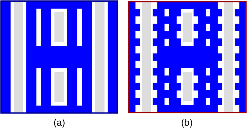 Figure 2 shows a more realistic example involving 1-D grating patterns that span a wide range of pitches on a thin OMOG mask, both with assist features (pitches above 180 nm comprising one to four SRAFs), and without assist features (pitches below 180 nm), that are optimized to print approximately 40 nm at wafer scale.2 Best-focus positions are plotted for three cases, namely for conventional masks, and for masks whose orthoedge sizes and locations are optimized in two different modes to cancel phase distortions in the image. Orthoedges are seen to substantially align the focal ranges. Simulations of the fields diffracted by these photomasks were carried out with an finite difference time domain Maxwell solver,1 and the aerial image intensity across focal planes was computed using a commercial imaging solver. Fig. 2Position of best focus for one-dimensional gratings on thin Opaque MoSi Over Glass masks imaged with Disar illumination at 1.35 NA across pitch, for conventional mask patterns, and after applying orthoedges in two modes (“simple” and “optimized”). Disar polarization is transverse electric. 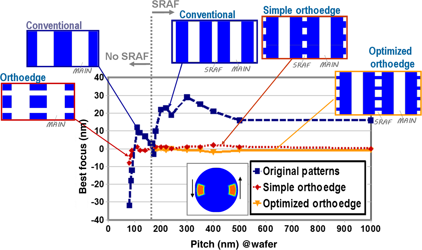 In Fig. 2, the plot of “original patterns” shows the impact on gratings above a 180-nm pitch of the conventional practice of uniformly aligning main feature edges and assist edges. A focus shift in the negative direction is also present for dense unassisted gratings below a 180-nm pitch. To correct these focus shifts, orthoedges were applied only on the SRAFs at assisted pitches above a 180-nm pitch, while dense, unassisted pitches were given orthoedges on the main feature. The masks in Fig. 2 labeled “simple orthoedge” are only optimized to minimize the range of best-focus positions across pitch, without consideration of any other lithographic metric. These masks achieved a greatly reduced spread of best focus in both assisted and unassisted patterns, with focus variation being virtually eliminated in assisted-only pitches. However, to maintain a good performance in other lithographic metrics, such as feature DoF, PW, mask error enhancement factor (MEEF), image log slope (ILS), and SRAF print-through suppression, it is generally necessary to co-optimize the mask shapes and the orthoedge parameters under formulations that consider a broad range of image requirements besides the spread in focus. The lengths of the orthogonal edges and the edge segments that connect to them can be treated as parameters, and suitable cancelation of phase distortions throughout the neighborhood of each feature edge can then be established by adjusting these parameters using optimization methodologies such as source mask optimization (SMO). The “optimized orthoedge” simulated results in Fig. 2 show that optimized orthoedge sizing and placement on assisted pitches can achieve similar performances in DoF, ILS, and MEEF as is achieved with conventionally assisted masks (see, e.g., Fig. 3), but without compromising the alignment of best-focus positions. This strongly favorable tradeoff is typically achieved whenever orthoedges are inserted into extended assist features. Orthoedges on the main features constitute an additional (fine) blurring of the defined edge, whose print location must be carefully controlled. Assists, on the other hand, must not print, but otherwise their amplitude on-wafer does not need to be finely set. Hence crenellation of 1-D feature edges in assists entails fewer tradeoffs than in main features. With 2-D random logic, a sophisticated optimization strategy can balance the tradeoffs between different metrics, as is desirable when orthoedges are deployed in main features. For example, EMF-aware SMO optimization of hammerhead line terminations shows that the tradeoffs of interest have a somewhat complex and unintuitive dependence on the detailed , fragmentation of the hammerheads, as we have described in Ref. 8. Fig. 3Initial image log slope performance loss with naive orthoedge subresolution assist feature (SRAF) sizing (keeping original SRAF size) is fully recovered after implementation of proper orthoedged SRAF optimization. 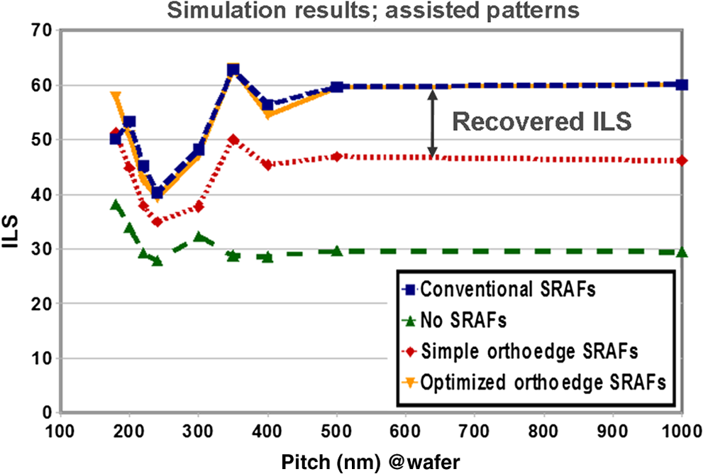 Although orthoedge optimization provides detailed control of these tradeoffs on a feature-by-feature basis, an increase in shot count is necessarily incurred. However, optimization can synergistically encompass a globally scoped baseline pupil phase profile that is delivered postmask by the lens hardware, in combination with locally adjustable phase tuning from orthoedges. A compromise across pattern diversity must be accepted in the programmed wavefront itself, but phase distortions can be corrected on a per-feature basis using orthoedges. Future work will investigate the tradeoffs between image quality and polygon edge density that become possible when feature-specific correction from orthoedges is applied in conjunction with a suitably programmed pupil-phase baseline. In general, phase correction is a coherent process, so different corrective methods will not impact image quality separately when used together, and joint design becomes appropriate. SRAFs can make a significant contribution to EMF-induced phase shifts in 2-D patterns, especially when combined with -polarization. Even when the edges of a main feature on a mask have no dominant - or -orientation, the phase perturbations from extended mask edges (in main features or assists) can distort the image contribution from either illuminating polarization. An example using -polarized Cquad illumination is shown in Fig. 4. Figure 4(a) shows, as a reference, the simulated “Bossung” plot of densely spaced square contacts in a staggered 2-D array, for which the central plane of best focus is found to be shifted by a relatively small from the TMA nominal. Figure 4(b) shows the Bossung plot of an isolated 2-D contact on the same mask when conventional assist features are used; the Bossungs are seen to be centered at around defocus in this case. Without assists, this focus shift would have been reduced to about , but the DOF for this pattern would then have decreased by about 20%. Finally, Fig. 4(c) illustrates the same isolated pattern as Fig. 4(b), where orthoedges have been applied and optimized for good lithographic performance. The orthoedges have nearly eliminated the focus shift (reducing it to ), while slightly extending the increase in feature DOF provided by Fig. 4(b) SRAFs. Mask corner rounding is neglected in these simulations, but rounding will not necessarily be deleterious if it merely merges the quadrature contributions of the orthoedges and the segments that connect them. Fig. 4Focus shift correction for contacts. (a) Dense staggered contact pattern, (b) isolated contact pattern assisted with conventional SRAFs, and (c) isolated assisted contact pattern with orthoedged SRAFs. 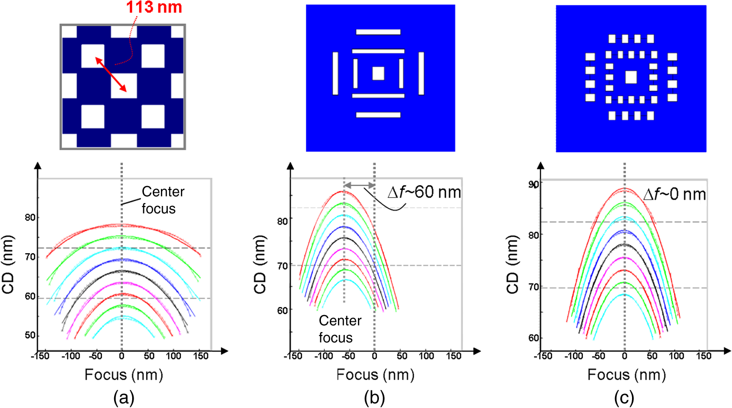 To sum up, orthoedges provide locally tailored phase compensation with state-of-the-art mask blank choices employing standard mask-making processes, allowing phase distortions in the overall imaging process to be mitigated by suitable layout design. AcknowledgmentsThis work was supported by the Semiconductor Research and Development Center in Hopewell Junction, New York, and by IBM Research, Brazil. ReferencesJ. Tirapu-Azpirozet al.,
“Massively-parallel FDTD simulations to address mask electromagnetic effects in hyper-NA immersion lithography,”
Proc. SPIE, 6924 69240Y
(2008). http://dx.doi.org/10.1117/12.774443 PSISDG 0277-786X Google Scholar
J. Tirapu-AzpirozA. E. Rosenbluth,
“Impact of sub-wavelength electromagnetic diffraction in optical lithography for semiconductor chip manufacturing,”
in SBMO/IEEE MTT-S Int. Microwave and Optoelectronics Conf.,
(2013). Google Scholar
F. Staalset al.,
“Advanced wavefront engineering for improved imaging and overlay applications on a 1.35 NA immersion scanner,”
Proc. SPIE, 7973 79731G
(2011). http://dx.doi.org/10.1117/12.880759 PSISDG 0277-786X Google Scholar
T. Faureet al.,
“Development and characterization of a thinner binary mask absorber for 22 nm node and beyond,”
Proc. SPIE, 7823 78230J
(2010). http://dx.doi.org/10.1117/12.864130 PSISDG 0277-786X Google Scholar
J. Tirapu-Azpirozet al.,
“Understanding the trade-offs of thinner binary mask absorbers,”
Proc. SPIE, 7823 78230M
(2010). http://dx.doi.org/10.1117/12.865358 PSISDG 0277-786X Google Scholar
J. Tirapu-AzpirozE. Yablonovitch,
“Incorporating mask topography edge diffraction in photolithography simulations,”
J. Opt. Soc. Am. A, 23
(4), 821
–828
(2006). http://dx.doi.org/10.1364/JOSAA.23.000821 JOAOD6 0740-3232 Google Scholar
D. O. Melvilleet al.,
“Demonstrating the benefits of SMO and enabling technologies through experiment and simulations,”
Proc. SPIE, 7640 764006
(2010). http://dx.doi.org/10.1117/12.846716 PSISDG 0277-786X Google Scholar
BiographyJaione Tirapu-Azpiroz received her PhD degree in electrical engineering from the University of California, Los Angeles, with Professor Eli Yablonovitch in 2004, and her master’s degree in telecommunication engineering from the Public University of Navarre, Spain. She has been a researcher with IBM Research—Brazil since 2012. She joined IBM in 2004 at the Semiconductor Research and Development Center (SRDC) in East Fishkill, New York. Alan E. Rosenbluth received a PhD degree in optics from the University of Rochester in 1982, as a Hertz Foundation Fellow. In the same year, he joined the IBM Thomas J. Watson Research Center. His primary research activities have been in photolithography, display technology, and soft x-ray optics. He has published many technical papers in these fields and holds 88 U.S. patents. Timothy Brunner received his BA degree from Carleton College in 1975 and a doctorate from MIT in 1980, both in physics. He has been a research scientist in the IBM Research Division, East Fishkill, New York, for over 20 years, working in the area of lithographic patterning for IC production—a most fascinating, interdisciplinary area. Before joining IBM in 1988, he worked for Perkin-Elmer Corporation and Xerox PARC. |


